WO2012121398A1 - 多環芳香族化合物 - Google Patents
多環芳香族化合物 Download PDFInfo
- Publication number
- WO2012121398A1 WO2012121398A1 PCT/JP2012/056206 JP2012056206W WO2012121398A1 WO 2012121398 A1 WO2012121398 A1 WO 2012121398A1 JP 2012056206 W JP2012056206 W JP 2012056206W WO 2012121398 A1 WO2012121398 A1 WO 2012121398A1
- Authority
- WO
- WIPO (PCT)
- Prior art keywords
- group
- groups
- substituted
- mono
- aryl
- Prior art date
Links
- 0 c(cc1*2c(cccc3)c3-c3ccccc3*22)ccc1-c1c2cccc1 Chemical compound c(cc1*2c(cccc3)c3-c3ccccc3*22)ccc1-c1c2cccc1 0.000 description 4
- RKMGAJGJIURJSJ-UHFFFAOYSA-N CC1(C)NC(C)(C)CCC1 Chemical compound CC1(C)NC(C)(C)CCC1 RKMGAJGJIURJSJ-UHFFFAOYSA-N 0.000 description 2
- PMZYJBTWBXSKLN-UHFFFAOYSA-N O=P1(c(cccc2)c2-c2ccccc22)N2c(cccc2)c2-c2ccccc12 Chemical compound O=P1(c(cccc2)c2-c2ccccc22)N2c(cccc2)c2-c2ccccc12 PMZYJBTWBXSKLN-UHFFFAOYSA-N 0.000 description 1
- MSQSOFDWOJYRHA-UHFFFAOYSA-N c(cc1)cc2c1-c(cccc1)c1N1c3cccc(N4c(cccc5N(B67)c8ccccc8-c8c6cccc8)c5-c5c7cccc5B44)c3-c3c4cccc3B21 Chemical compound c(cc1)cc2c1-c(cccc1)c1N1c3cccc(N4c(cccc5N(B67)c8ccccc8-c8c6cccc8)c5-c5c7cccc5B44)c3-c3c4cccc3B21 MSQSOFDWOJYRHA-UHFFFAOYSA-N 0.000 description 1
- UWSKGRGARWPYHG-UHFFFAOYSA-N c(cc1)ccc1-c(cccc1)c1Nc1c(-c2ccccc2)c(Nc2cccc(Nc(cccc3)c3-c3ccccc3)c2-c2ccccc2)ccc1 Chemical compound c(cc1)ccc1-c(cccc1)c1Nc1c(-c2ccccc2)c(Nc2cccc(Nc(cccc3)c3-c3ccccc3)c2-c2ccccc2)ccc1 UWSKGRGARWPYHG-UHFFFAOYSA-N 0.000 description 1
- CCVPAHODKCQOET-UHFFFAOYSA-N c(cc1)ccc1-c1ccccc1Nc(cccc1)c1-c(cc1)ccc1-c(cccc1)c1Nc(cccc1)c1-c1ccccc1 Chemical compound c(cc1)ccc1-c1ccccc1Nc(cccc1)c1-c(cc1)ccc1-c(cccc1)c1Nc(cccc1)c1-c1ccccc1 CCVPAHODKCQOET-UHFFFAOYSA-N 0.000 description 1
- VSHCBMSTHBJECK-UHFFFAOYSA-N c(cc1-c2c3cccc2)ccc1N1P3c2ccccc2-c2c1cccc2 Chemical compound c(cc1-c2c3cccc2)ccc1N1P3c2ccccc2-c2c1cccc2 VSHCBMSTHBJECK-UHFFFAOYSA-N 0.000 description 1
- WXHWSRPRAFALPC-UHFFFAOYSA-N c(cc1B23)ccc1-c(cccc1)c1N2c(cccc1)c1-c(cc1B24)c3cc1-c(cccc1)c1N2c1ccccc1-c1c4cccc1 Chemical compound c(cc1B23)ccc1-c(cccc1)c1N2c(cccc1)c1-c(cc1B24)c3cc1-c(cccc1)c1N2c1ccccc1-c1c4cccc1 WXHWSRPRAFALPC-UHFFFAOYSA-N 0.000 description 1
Classifications
-
- C—CHEMISTRY; METALLURGY
- C07—ORGANIC CHEMISTRY
- C07F—ACYCLIC, CARBOCYCLIC OR HETEROCYCLIC COMPOUNDS CONTAINING ELEMENTS OTHER THAN CARBON, HYDROGEN, HALOGEN, OXYGEN, NITROGEN, SULFUR, SELENIUM OR TELLURIUM
- C07F5/00—Compounds containing elements of Groups 3 or 13 of the Periodic System
- C07F5/02—Boron compounds
-
- C—CHEMISTRY; METALLURGY
- C07—ORGANIC CHEMISTRY
- C07F—ACYCLIC, CARBOCYCLIC OR HETEROCYCLIC COMPOUNDS CONTAINING ELEMENTS OTHER THAN CARBON, HYDROGEN, HALOGEN, OXYGEN, NITROGEN, SULFUR, SELENIUM OR TELLURIUM
- C07F7/00—Compounds containing elements of Groups 4 or 14 of the Periodic System
- C07F7/02—Silicon compounds
- C07F7/08—Compounds having one or more C—Si linkages
- C07F7/10—Compounds having one or more C—Si linkages containing nitrogen having a Si-N linkage
-
- C—CHEMISTRY; METALLURGY
- C07—ORGANIC CHEMISTRY
- C07F—ACYCLIC, CARBOCYCLIC OR HETEROCYCLIC COMPOUNDS CONTAINING ELEMENTS OTHER THAN CARBON, HYDROGEN, HALOGEN, OXYGEN, NITROGEN, SULFUR, SELENIUM OR TELLURIUM
- C07F7/00—Compounds containing elements of Groups 4 or 14 of the Periodic System
- C07F7/22—Tin compounds
- C07F7/2284—Compounds with one or more Sn-N linkages
-
- C—CHEMISTRY; METALLURGY
- C07—ORGANIC CHEMISTRY
- C07F—ACYCLIC, CARBOCYCLIC OR HETEROCYCLIC COMPOUNDS CONTAINING ELEMENTS OTHER THAN CARBON, HYDROGEN, HALOGEN, OXYGEN, NITROGEN, SULFUR, SELENIUM OR TELLURIUM
- C07F7/00—Compounds containing elements of Groups 4 or 14 of the Periodic System
- C07F7/30—Germanium compounds
-
- C—CHEMISTRY; METALLURGY
- C07—ORGANIC CHEMISTRY
- C07F—ACYCLIC, CARBOCYCLIC OR HETEROCYCLIC COMPOUNDS CONTAINING ELEMENTS OTHER THAN CARBON, HYDROGEN, HALOGEN, OXYGEN, NITROGEN, SULFUR, SELENIUM OR TELLURIUM
- C07F9/00—Compounds containing elements of Groups 5 or 15 of the Periodic System
- C07F9/02—Phosphorus compounds
- C07F9/547—Heterocyclic compounds, e.g. containing phosphorus as a ring hetero atom
- C07F9/6564—Heterocyclic compounds, e.g. containing phosphorus as a ring hetero atom having phosphorus atoms, with or without nitrogen, oxygen, sulfur, selenium or tellurium atoms, as ring hetero atoms
- C07F9/6581—Heterocyclic compounds, e.g. containing phosphorus as a ring hetero atom having phosphorus atoms, with or without nitrogen, oxygen, sulfur, selenium or tellurium atoms, as ring hetero atoms having phosphorus and nitrogen atoms with or without oxygen or sulfur atoms, as ring hetero atoms
- C07F9/6584—Heterocyclic compounds, e.g. containing phosphorus as a ring hetero atom having phosphorus atoms, with or without nitrogen, oxygen, sulfur, selenium or tellurium atoms, as ring hetero atoms having phosphorus and nitrogen atoms with or without oxygen or sulfur atoms, as ring hetero atoms having one phosphorus atom as ring hetero atom
- C07F9/65842—Cyclic amide derivatives of acids of phosphorus, in which one nitrogen atom belongs to the ring
- C07F9/65846—Cyclic amide derivatives of acids of phosphorus, in which one nitrogen atom belongs to the ring the phosphorus atom being part of a six-membered ring which may be condensed with another ring system
-
- C—CHEMISTRY; METALLURGY
- C07—ORGANIC CHEMISTRY
- C07F—ACYCLIC, CARBOCYCLIC OR HETEROCYCLIC COMPOUNDS CONTAINING ELEMENTS OTHER THAN CARBON, HYDROGEN, HALOGEN, OXYGEN, NITROGEN, SULFUR, SELENIUM OR TELLURIUM
- C07F9/00—Compounds containing elements of Groups 5 or 15 of the Periodic System
- C07F9/02—Phosphorus compounds
- C07F9/547—Heterocyclic compounds, e.g. containing phosphorus as a ring hetero atom
- C07F9/6564—Heterocyclic compounds, e.g. containing phosphorus as a ring hetero atom having phosphorus atoms, with or without nitrogen, oxygen, sulfur, selenium or tellurium atoms, as ring hetero atoms
- C07F9/6581—Heterocyclic compounds, e.g. containing phosphorus as a ring hetero atom having phosphorus atoms, with or without nitrogen, oxygen, sulfur, selenium or tellurium atoms, as ring hetero atoms having phosphorus and nitrogen atoms with or without oxygen or sulfur atoms, as ring hetero atoms
- C07F9/6587—Heterocyclic compounds, e.g. containing phosphorus as a ring hetero atom having phosphorus atoms, with or without nitrogen, oxygen, sulfur, selenium or tellurium atoms, as ring hetero atoms having phosphorus and nitrogen atoms with or without oxygen or sulfur atoms, as ring hetero atoms having two phosphorus atoms as ring hetero atoms in the same ring
-
- C—CHEMISTRY; METALLURGY
- C09—DYES; PAINTS; POLISHES; NATURAL RESINS; ADHESIVES; COMPOSITIONS NOT OTHERWISE PROVIDED FOR; APPLICATIONS OF MATERIALS NOT OTHERWISE PROVIDED FOR
- C09B—ORGANIC DYES OR CLOSELY-RELATED COMPOUNDS FOR PRODUCING DYES, e.g. PIGMENTS; MORDANTS; LAKES
- C09B57/00—Other synthetic dyes of known constitution
-
- C—CHEMISTRY; METALLURGY
- C09—DYES; PAINTS; POLISHES; NATURAL RESINS; ADHESIVES; COMPOSITIONS NOT OTHERWISE PROVIDED FOR; APPLICATIONS OF MATERIALS NOT OTHERWISE PROVIDED FOR
- C09K—MATERIALS FOR MISCELLANEOUS APPLICATIONS, NOT PROVIDED FOR ELSEWHERE
- C09K11/00—Luminescent, e.g. electroluminescent, chemiluminescent materials
- C09K11/06—Luminescent, e.g. electroluminescent, chemiluminescent materials containing organic luminescent materials
-
- H—ELECTRICITY
- H05—ELECTRIC TECHNIQUES NOT OTHERWISE PROVIDED FOR
- H05B—ELECTRIC HEATING; ELECTRIC LIGHT SOURCES NOT OTHERWISE PROVIDED FOR; CIRCUIT ARRANGEMENTS FOR ELECTRIC LIGHT SOURCES, IN GENERAL
- H05B33/00—Electroluminescent light sources
- H05B33/12—Light sources with substantially two-dimensional radiating surfaces
- H05B33/14—Light sources with substantially two-dimensional radiating surfaces characterised by the chemical or physical composition or the arrangement of the electroluminescent material, or by the simultaneous addition of the electroluminescent material in or onto the light source
-
- H—ELECTRICITY
- H10—SEMICONDUCTOR DEVICES; ELECTRIC SOLID-STATE DEVICES NOT OTHERWISE PROVIDED FOR
- H10K—ORGANIC ELECTRIC SOLID-STATE DEVICES
- H10K30/00—Organic devices sensitive to infrared radiation, light, electromagnetic radiation of shorter wavelength or corpuscular radiation
-
- H—ELECTRICITY
- H10—SEMICONDUCTOR DEVICES; ELECTRIC SOLID-STATE DEVICES NOT OTHERWISE PROVIDED FOR
- H10K—ORGANIC ELECTRIC SOLID-STATE DEVICES
- H10K85/00—Organic materials used in the body or electrodes of devices covered by this subclass
- H10K85/30—Coordination compounds
-
- H—ELECTRICITY
- H10—SEMICONDUCTOR DEVICES; ELECTRIC SOLID-STATE DEVICES NOT OTHERWISE PROVIDED FOR
- H10K—ORGANIC ELECTRIC SOLID-STATE DEVICES
- H10K85/00—Organic materials used in the body or electrodes of devices covered by this subclass
- H10K85/30—Coordination compounds
- H10K85/321—Metal complexes comprising a group IIIA element, e.g. Tris (8-hydroxyquinoline) gallium [Gaq3]
- H10K85/322—Metal complexes comprising a group IIIA element, e.g. Tris (8-hydroxyquinoline) gallium [Gaq3] comprising boron
-
- H—ELECTRICITY
- H10—SEMICONDUCTOR DEVICES; ELECTRIC SOLID-STATE DEVICES NOT OTHERWISE PROVIDED FOR
- H10K—ORGANIC ELECTRIC SOLID-STATE DEVICES
- H10K85/00—Organic materials used in the body or electrodes of devices covered by this subclass
- H10K85/40—Organosilicon compounds, e.g. TIPS pentacene
-
- H—ELECTRICITY
- H10—SEMICONDUCTOR DEVICES; ELECTRIC SOLID-STATE DEVICES NOT OTHERWISE PROVIDED FOR
- H10K—ORGANIC ELECTRIC SOLID-STATE DEVICES
- H10K85/00—Organic materials used in the body or electrodes of devices covered by this subclass
- H10K85/60—Organic compounds having low molecular weight
- H10K85/649—Aromatic compounds comprising a hetero atom
- H10K85/657—Polycyclic condensed heteroaromatic hydrocarbons
-
- C—CHEMISTRY; METALLURGY
- C09—DYES; PAINTS; POLISHES; NATURAL RESINS; ADHESIVES; COMPOSITIONS NOT OTHERWISE PROVIDED FOR; APPLICATIONS OF MATERIALS NOT OTHERWISE PROVIDED FOR
- C09K—MATERIALS FOR MISCELLANEOUS APPLICATIONS, NOT PROVIDED FOR ELSEWHERE
- C09K2211/00—Chemical nature of organic luminescent or tenebrescent compounds
- C09K2211/10—Non-macromolecular compounds
- C09K2211/1018—Heterocyclic compounds
- C09K2211/1025—Heterocyclic compounds characterised by ligands
- C09K2211/1029—Heterocyclic compounds characterised by ligands containing one nitrogen atom as the heteroatom
- C09K2211/104—Heterocyclic compounds characterised by ligands containing one nitrogen atom as the heteroatom with other heteroatoms
-
- H—ELECTRICITY
- H10—SEMICONDUCTOR DEVICES; ELECTRIC SOLID-STATE DEVICES NOT OTHERWISE PROVIDED FOR
- H10K—ORGANIC ELECTRIC SOLID-STATE DEVICES
- H10K10/00—Organic devices specially adapted for rectifying, amplifying, oscillating or switching; Organic capacitors or resistors having a potential-jump barrier or a surface barrier
- H10K10/40—Organic transistors
- H10K10/46—Field-effect transistors, e.g. organic thin-film transistors [OTFT]
- H10K10/462—Insulated gate field-effect transistors [IGFETs]
- H10K10/484—Insulated gate field-effect transistors [IGFETs] characterised by the channel regions
-
- H—ELECTRICITY
- H10—SEMICONDUCTOR DEVICES; ELECTRIC SOLID-STATE DEVICES NOT OTHERWISE PROVIDED FOR
- H10K—ORGANIC ELECTRIC SOLID-STATE DEVICES
- H10K50/00—Organic light-emitting devices
- H10K50/10—OLEDs or polymer light-emitting diodes [PLED]
- H10K50/11—OLEDs or polymer light-emitting diodes [PLED] characterised by the electroluminescent [EL] layers
-
- H—ELECTRICITY
- H10—SEMICONDUCTOR DEVICES; ELECTRIC SOLID-STATE DEVICES NOT OTHERWISE PROVIDED FOR
- H10K—ORGANIC ELECTRIC SOLID-STATE DEVICES
- H10K50/00—Organic light-emitting devices
- H10K50/10—OLEDs or polymer light-emitting diodes [PLED]
- H10K50/14—Carrier transporting layers
- H10K50/15—Hole transporting layers
-
- H—ELECTRICITY
- H10—SEMICONDUCTOR DEVICES; ELECTRIC SOLID-STATE DEVICES NOT OTHERWISE PROVIDED FOR
- H10K—ORGANIC ELECTRIC SOLID-STATE DEVICES
- H10K50/00—Organic light-emitting devices
- H10K50/10—OLEDs or polymer light-emitting diodes [PLED]
- H10K50/14—Carrier transporting layers
- H10K50/16—Electron transporting layers
-
- Y—GENERAL TAGGING OF NEW TECHNOLOGICAL DEVELOPMENTS; GENERAL TAGGING OF CROSS-SECTIONAL TECHNOLOGIES SPANNING OVER SEVERAL SECTIONS OF THE IPC; TECHNICAL SUBJECTS COVERED BY FORMER USPC CROSS-REFERENCE ART COLLECTIONS [XRACs] AND DIGESTS
- Y02—TECHNOLOGIES OR APPLICATIONS FOR MITIGATION OR ADAPTATION AGAINST CLIMATE CHANGE
- Y02E—REDUCTION OF GREENHOUSE GAS [GHG] EMISSIONS, RELATED TO ENERGY GENERATION, TRANSMISSION OR DISTRIBUTION
- Y02E10/00—Energy generation through renewable energy sources
- Y02E10/50—Photovoltaic [PV] energy
- Y02E10/549—Organic PV cells
Definitions
- the present invention relates to a novel compound, and more specifically, a polycyclic aromatic compound containing a nitrogen atom and another heteroatom or metal atom, an organic light-emitting element such as an organic EL device or an organic light-emitting diode containing the compound, an organic thin film transistor, an organic thin film
- an electrochemical device such as a thin film solar cell.
- a thin film containing a fluorescent organic compound or a phosphorescent organic compound is sandwiched between an anode and a cathode. It is an element that uses light emitted when excitons of fluorescent compounds or phosphorescent compounds are generated by injecting electrons and holes (holes) from each electrode, and these excitons return to the ground state. .
- Patent Document 4 discloses a polycyclic aromatic compound having one hetero atom in a non-aromatic ring.
- An object of the present invention is to provide a novel polycyclic aromatic compound and an electrochemical device such as an organic light emitting device, an organic thin film transistor, or an organic thin film solar cell containing the compound.
- the present inventor has developed a novel polycyclic aromatic compound in which a nitrogen atom and another heteroatom or metal atom (X) are adjacent in a non-aromatic ring, an organic light-emitting device containing the compound, an organic thin film transistor, an organic thin film solar cell, etc.
- An electrochemical device is provided.
- Item 1 The polycyclic aromatic compound or its salt which has the partial structure represented by the following general formula (I).
- a ring, B ring, C ring and D ring are the same or different and each represents an optionally substituted aromatic ring or an optionally substituted heteroaromatic ring.
- Item 2. The polycyclic aromatic compound or a salt thereof according to item 1, having a partial structure represented by the following general formula (II).
- Item 3. The polycyclic aromatic compound or a salt thereof according to item 1 or 2, which has a partial structure represented by the following general formula (II-1).
- Item 4. The polycyclic aromatic compound or a salt thereof according to any one of Items 1 to 3, having a partial structure represented by any one of the following general formulas (II-2) to (II-54).
- Item 5 The polycyclic aromatic compound or a salt thereof according to any one of Items 1 to 4 represented by the following general formula (II ′).
- Y is the same or different and represents CR or N, or two adjacent Ys in the same ring each together with a bond between them represent NR, O, S or Se.
- halogen atom hydroxy group, C 1-20 alkoxy group, an aryloxy group, an amino group, a carbazole group, N (R a) 2 (the R a are as defined above), triflic Romechiru group, C 2-12 perfluoroalkyl group, C 3-8 cycloalkyl group, may be substituted with 1 to 3 atoms or groups selected from aryl and heteroaryl groups, and said aryl Group, aryl moiety, heteroaryl group, heteroaryl moiety, carbazole group are a halogen atom, a C 1-20 alkyl group, a hydroxy C 1-20 alkyl group, a trifluoromethyl group, a C 2-12 perfluoroalkyl group, a C 3-8 cycloalkyl group, C 2-20 alkenyl group, C 2-20 alkynyl group, mono- or diaryl-substituted alkenyl group, mono- or diheteroaryl-
- two adjacent R groups may be monocyclic, bicyclic, or optionally have a 5- or 6-membered heteroatom together with the carbon atom to which they are attached.
- 3 represents a tricyclic group
- three adjacent R groups represent a bicyclic group or a tricyclic group which may have a hetero atom together with the carbon atom to which they are bonded.
- the two R groups are single bonds, CH 2 , CHR a , CR a 2 , NR a , Si (R a ) 2 , BR a (R a Is as defined above), Se, S or O. )
- Item 6. The polycyclic aromatic compound or a salt thereof according to any one of Items 1 to 5 represented by the following general formula (II′-1).
- the alkyl group, alkenyl group, alkynyl group and alkoxy group are a halogen atom, hydroxy group, C 1-20 alkoxy group, aryloxy group, amino group, carbazole group, N (R a ) 2 (R a is as defined above.
- a Rutori substituted with a trifluoromethyl group, C 2-12 perfluoroalkyl group, C 3-8 cycloalkyl group, one to three atoms or groups selected from aryl and heteroaryl groups And may, also be, the aryl group, the aryl moiety, the heteroaryl group, the heteroaryl moiety, a carbazole group, a halogen atom, C 1-20 alkyl, hydroxyalkyl C 1-20 alkyl group, a trifluoromethyl group, C 2-12 perfluoroalkyl group, C 3-8 cycloalkyl group, C 2-20 alkenyl group, C 2-20 alkynyl group, mono or diaryl substituted alkenyl group, mono or diheteroaryl substituted alkenyl group, aryl ethynyl group , Heteroarylethynyl group, hydroxy group, C 1-20 alkoxy group, aryloxy group, trifluoromethoxy group,
- two adjacent R groups may be monocyclic, bicyclic, or optionally have a 5- or 6-membered heteroatom together with the carbon atom to which they are attached.
- 3 represents a tricyclic group
- three adjacent R groups represent a bicyclic group or a tricyclic group which may have a hetero atom together with the carbon atom to which they are bonded.
- the two R groups are single bonds, CH 2 , CHR a , CR a 2 , NR a , Si (R a ) 2 , BR a (R a Is as defined above), Se, S or O. )
- Item 7. The polycyclic aromatic compound or a salt thereof according to any one of Items 1 to 6 represented by the following general formulas (III ′) to (XXIII ′):
- Y is the same or different and represents CR, N, or two adjacent Ys in the same ring each together with a bond between them represents NR, O, S or Se.
- two adjacent R groups may be monocyclic, bicyclic, or optionally have a 5- or 6-membered heteroatom together with the carbon atom to which they are attached.
- 3 represents a tricyclic group, and three adjacent R groups represent a bicyclic group or a tricyclic group which may have a hetero atom together with the carbon atom to which they are bonded.
- the two R groups are single bonds, CH 2 , CHR a , CR a 2 , NR a , Si (R a ) 2 , BR a (R a Is as defined above), Se, S or O. )
- Item 8 The compound according to any one of Items 1 to 7, represented by any one of the following formulas (II′-1A) to (XIV′-1A):
- the alkyl group, alkenyl group, alkynyl group and alkoxy group are a halogen atom, hydroxy group, C 1-20 alkoxy group, aryloxy group, amino group, carbazole group, N (R a ) 2 (R a is as defined above.
- a Rutori substituted with a trifluoromethyl group, C 2-12 perfluoroalkyl group, C 3-8 cycloalkyl group, one to three atoms or groups selected from aryl and heteroaryl groups And may, also be, the aryl group, the aryl moiety, the heteroaryl group, the heteroaryl moiety, a carbazole group, a halogen atom, C 1-20 alkyl, hydroxyalkyl C 1-20 alkyl group, a trifluoromethyl group, C 2-12 perfluoroalkyl group, C 3-8 cycloalkyl group, C 2-20 alkenyl group, C 2-20 alkynyl group, mono or diaryl substituted alkenyl group, mono or diheteroaryl substituted alkenyl group, aryl ethynyl group , Heteroarylethynyl group, hydroxy group, C 1-20 alkoxy group, aryloxy group, trifluoromethoxy group,
- two adjacent R groups may be monocyclic, bicyclic, or optionally have a 5- or 6-membered heteroatom together with the carbon atom to which they are attached.
- 3 represents a tricyclic group
- three adjacent R groups represent a bicyclic group or a tricyclic group which may have a hetero atom together with the carbon atom to which they are bonded.
- the two R groups are single bonds, CH 2 , CHR a , CR a 2 , NR a , Si (R a ) 2 , BR a (R a Is as defined above), Se, S or O. )
- Item 9 An electrochemical device comprising the compound according to any one of Items 1 to 8.
- Item 10 is an organic light emitting device, an organic thin film transistor, or an organic thin film solar cell.
- novel compounds such as hole transport materials, light-emitting materials, and electron transport materials suitable for use in organic light-emitting elements such as organic EL devices and organic light-emitting diodes, organic thin-film transistors, and organic thin-film solar cells can be obtained.
- organic light-emitting elements such as organic EL devices and organic light-emitting diodes, organic thin-film transistors, and organic thin-film solar cells.
- Y a is the same or different and each represents C— or N, or two Y a adjacent to each other in the same ring are each combined with a bond between them, N—, O, S Or Se represents Y or C—R or N, which are the same or different, or two Ys adjacent in the same ring together with a bond between them each represent NR, O, S or Se Indicates.
- Y and Y a are corresponding groups, but since Y a is used for the partial structure, the R group is not included.
- the present invention provides a polycyclic aromatic compound having a partial structure represented by the following general formula (I) or a salt thereof.
- One preferable embodiment of the present invention is a polycyclic aromatic compound having a partial structure represented by the following general formula (II) or a salt thereof.
- One preferable embodiment of the present invention is a polycyclic aromatic compound having a partial structure represented by the following general formula (II-1) or a salt thereof.
- Another preferred embodiment of the present invention is a polycyclic aromatic compound having a partial structure represented by the following general formulas (II-2) to (II-54) or a salt thereof.
- Examples of the compound having the partial structure represented by the general formula (I) include compounds having the following skeletons 1 to 149 (these compounds may be further substituted).
- Examples of the metal of Group 3 to 11 of the periodic table, the metal or metalloid of Groups 13 to 14 of the periodic table represented by X include the following.
- a metal of Group 3 to 11 of the periodic table, a metal or metalloid of Groups 13 to 14 of the periodic table represented by X, Each may be substituted.
- these metals or semi-metals may be “substituted” by 0 to 3 substituents R (where R is as defined above), or 0 to 3 neutrals. It means that it may have the ligand R 1 of Examples of the neutral ligand R 1 include aromatic compounds having a nitrogen atom as a ring atom, such as pyridine, bipyridine, phenanthroline, terpyridine, imidazole, pyrimidine, pyrazine, quinoline, isoquinoline, and acridine, and derivatives thereof.
- R and R 1 may be formed by a single compound (8-hydroxyquinoline) as follows Case (3).
- the compound having a neutral ligand R 1 can be produced, for example, as follows.
- Case (1) represents a case where a neutral ligand (R 1 ) is bonded to X (metal or semimetal) of (I) to obtain (I ′) compound.
- a compound having a neutral ligand can be easily produced by those skilled in the art with reference to the above Case (1) to Case (3).
- X 1 and X 2 can be changed when the electronegativity is approximately the same or in a combination where X 1 ⁇ X 2 .
- X 1 Ge—R
- X 2 can be B
- P, P O
- P S
- P Se
- As, As O
- As S
- As Se
- Mo W
- Ru Os
- Rh Ir
- Pd Pt
- Au Au
- Solvents include anhydrous ether solvents such as anhydrous diethyl ether, anhydrous THF, and anhydrous dibutyl ether, aromatic hydrocarbon solvents such as benzene, toluene, xylene, mesitylene, and aromatics such as chlorobenzene and 1,2-dichlorobenzene.
- Anhydrous ether solvents such as anhydrous diethyl ether, anhydrous THF, and anhydrous dibutyl ether
- aromatic hydrocarbon solvents such as benzene, toluene, xylene, mesitylene
- aromatics such as chlorobenzene and 1,2-dichlorobenzene.
- a halide solvent is used.
- Lewis acids examples include AlCl 3 , AlBr 3 , BF 3 .OEt 2 , BCl 3 , BBr 3 , GaCl 3 , GaBr 3 , InCl 3 , InBr 3 , In (OTf) 3 , SnCl 4 , SnBr 4 f, AgT (OTf) 3 , ZnCl 2 , ZnBr 2 , Zn (OTf) 2 , MgCl 2 , MgBr 2 , Mg (OTf) 2, or the like is used.
- Bases include diisopropylethylamine, 2,2,6,6, -tetramethylpiperidine, 1,2,2,6,6, -pentamethylpiperidine, 2,4,6-collidine, 2,6-lutidine, triethylamine , Triisobutylamine and the like are used.
- Preferred X groups include B, P, P ⁇ O, P ⁇ S, Si—R, Ge—R, Ga, Pt, Ru, Ir, Au, and the like.
- adjacent R groups may be adjacent groups in the same ring, or may be the closest R groups in adjacent rings.
- aromatic ring of “optionally substituted aromatic ring” includes benzene ring, naphthalene ring, azulene ring, biphenylene ring, fluorene ring, anthracene ring, indacene ring, phenanthrene ring, phenalene ring, pyrene ring, chrysene ring, triphenylene Ring, fluoranthene ring, acephenanthrylene ring, aceantolylene ring, picene ring, naphthacene ring, perylene ring, acenaphthylene ring, acenaphthene ring, indane ring, indene ring, and tetrahydronaphthalene ring.
- heteroaromatic ring of the “optionally substituted heteroaromatic ring” examples include furan ring, thiophene ring, selenophene ring, pyrrole ring, imidazole ring, thiazole ring, isothiazole ring, oxazole ring, isoxazole ring, triazole ring, Borol ring, phosphole ring, silole ring, azaborine ring, pyridine ring, pyrimidine ring, triazine ring, pyran ring, indole ring, isoindole ring, quinoline ring, isoquinoline ring, quinoxaline ring, benzoxazole ring, benzothiazole ring, benzoiso Oxazole ring, benzoisothiazole ring, benzofuran ring, benzothiophene ring, benzopyran ring, benzimidazole ring, benzoboron
- the number of substituents on the optionally substituted aromatic ring or optionally substituted heteroaromatic ring is 1 to 4, preferably 1, 2, or 3.
- substituents of the aromatic ring which may be substituted or the heteroaromatic ring which may be substituted include a group represented by R.
- Examples of the “monocyclic group, bicyclic group or tricyclic group optionally having a 5-membered or 6-membered hetero atom” include benzene, naphthalene, azulene, biphenylene, fluorene, anthracene, indacene, Phenanthrene, phenalene, acenaphthylene, acenaphthene, indane, indene, tetrahydronaphthalene, cyclopentadiene, cyclohexadiene, furan, thiophene, selenophene, pyrrole, imidazole, thiazole, isothiazole, oxazole, isoxazole, triazole, borol, phosphorol, silole, azaborine Pyridine, pyrimidine, triazine, pyran, indole, isoindole, quinoline, isoquinoline, qui
- R a is as defined above.
- a 5-membered or 6-membered ring group having an X group can be mentioned.
- Examples of the ⁇ bicyclic group or tricyclic group optionally having a hetero atom '' include naphthalene, azulene, biphenylene, fluorene, anthracene, indacene, phenanthrene, phenalene, acenaphthylene, acenaphthene, indane, indene, tetrahydronaphthalene, Indole, isoindole, quinoline, isoquinoline, quinoxaline, benzoxazole, benzothiazole, benzoisoxazole, benzoisothiazole, benzofuran, benzothiophene, benzopyran, benzimidazole, benzoborol, benzophosphole, benzosilol, benzoazaborine, indolizine, acridine, Phenazine, phenanthridine, phenanthroline, benzoselenophene, naphthofur
- the number of carbon atoms is defined as “C 1-20 alkylcarbonyl”, but this number of carbon atoms modifies only the group or moiety that immediately follows. Therefore, in the above case, since C 1-20 modifies only alkyl, “C 1 alkylcarbonyl” corresponds to acetyl.
- the alkyl group and the alkyl moiety may be linear or branched.
- the alkyl moiety means an optionally substituted alkyl group, a C 1-20 alkylsulfonyl group, a C 1-20 alkylsulfonylamino group, a C 1-20 alkylcarbonylamino group, and a C 1-20 alkylcarbonyl. It includes not only each alkyl group in the group but also an alkyl group that is a substituent of a monoalkylamino group, a mono- or di-alkylsulfamoyl group, or a mono- or di-alkylcarbamoyl group.
- the aryl moiety means a mono- or diaryl-substituted alkenyl group, an arylethynyl group, an aryloxy group, a monoarylamino group, or an aryl group which may be substituted.
- the heteroaryl moiety means a heteroaryl group of a monoheteroarylamino group, a mono- or heteroaryl-substituted alkenyl group, a heteroarylethynyl group, or an optionally substituted heteroaryl group.
- Halogen atom means fluorine, chlorine, bromine or iodine, preferably fluorine, chlorine or bromine.
- the “C 1-20 alkyl group” may be any of linear, branched or cyclic, for example, methyl group, ethyl group, n-propyl group, isopropyl group, n-butyl group, isobutyl group, C 1- such as tert-butyl, n-pentyl, isopentyl, hexyl, heptyl, octyl, nonyl, decyl, undecyl, dodecyl, tetradecyl, hexadecyl, octadecyl, eicosyl
- a 20 alkyl group preferably a C 1-10 alkyl group, more preferably a C 1-6 alkyl group can be mentioned.
- C 3-8 cycloalkyl group examples include a cyclopropyl group, a cyclobutyl group, a cyclopentyl group, a cyclohexyl group, a cycloheptyl group, and a cyclooctyl group.
- the “C 2-20 alkenyl group” may be linear, branched or cyclic, and means one having at least one double bond, for example, vinyl group, allyl group, 1-propenyl group. 2-methyl-2-propenyl group, isopropenyl group, 1-, 2- or 3-butenyl group, 2-, 3- or 4-pentenyl group, 2-methyl-2-butenyl group, 3-methyl-2 -Butenyl group, 5-hexenyl group, 1-cyclopentenyl group, 1-cyclohexenyl group, 3-methyl-3-butenyl group, preferably C 2-12 alkenyl group, more preferably C 2-6 alkenyl group Groups.
- the “C 2-20 alkynyl group” may be any of linear, branched or cyclic, and means having at least one triple bond, such as an ethynyl group, 1- or 2-propynyl group, 1-, 2- or 3-butynyl group, 1-methyl-2-propynyl group, 1-pentynyl group, 1-hexynyl group, 1-heptynyl group, 1-octynyl group, 1-nonenyl group, 1-decynyl group , 1-undecynyl group and 1-dodecynyl group, preferably C 2-10 alkynyl group, more preferably C 2-6 alkynyl group.
- the “hydroxy C 1-20 alkyl group” may be linear or branched.
- the “C 1-20 alkoxy group” may be linear or branched.
- CF 3 CH 2 O— is preferable.
- the “C 2-12 perfluoroalkyl group” may be linear or branched, and examples thereof include a perfluoroethyl group, a perfluoro n-propyl group, a perfluoroisopropyl group, and a perfluoro n-butyl group.
- perfluoroisobutyl group perfluoro tert-butyl group, perfluoro n-pentyl group, perfluoroisopentyl group, perfluorohexyl group, perfluoroheptyl group, perfluorooctyl group, perfluorononyl group, perfluorodecyl
- a C 2-12 perfluoroalkyl group such as a perfluoroundecyl group, preferably a C 2-10 perfluoroalkyl group, more preferably a C 2-6 perfluoroalkyl group.
- the “C 2-12 perfluoroalkoxy group” may be linear or branched, and examples thereof include a perfluoroethoxy group, a perfluoro n-propyloxy group, a perfluoroisopropyloxy group, and a perfluoro n group.
- the term “monoalkyl” in a monoalkylamino group, mono- or dialkylcarbamoyl group or mono- or dialkylsulfamoyl group means that one hydrogen atom bonded to the nitrogen atom of the amino group, carbamoyl group or sulfamoyl group is C 1-20.
- dialkyl means that two hydrogen atoms bonded to the nitrogen atom of the amino group, carbamoyl group or sulfamoyl group are substituted with the same or different C 1-20 alkyl. Or substituted with a 3- to 8-membered, preferably 5- or 6-membered, nitrogen-containing cyclic group.
- the nitrogen-containing cyclic group include a morpholino group, a 1-pyrrolidinyl group, a piperidino and a 4-methyl-1-piperazinyl group.
- the monoalkylamino group includes methylamino group, ethylamino group, n-propylamino group, isopropylamino group, n-butylamino group, isobutylamino group, tert-butylamino group, n-pentylamino group, isopentylamino group.
- an amino group monosubstituted by a C 1-20 alkyl group such as a hexylamino group, preferably a C 1-10 alkyl group, more preferably a C 1-6 alkyl group.
- Monoalkylcarbamoyl groups include methylcarbamoyl group, ethylcarbamoyl group, n-propylcarbamoyl group, isopropylcarbamoyl group, n-butylcarbamoyl group, isobutylcarbamoyl group, tert-butylcarbamoyl group, n-pentylcarbamoyl group, isopentylcarbamoyl group And a carbamoyl monosubstituted by a C 1-20 alkyl group such as a hexylcarbamoyl group, preferably a C 1-10 alkyl group, more preferably a C 1-6 alkyl group.
- dialkylcarbamoyl group examples include a dimethylcarbamoyl group, a diethylcarbamoyl group, a di-n-propylcarbamoyl group, a diisopropylcarbamoyl group, a din-butylcarbamoyl group, a diisobutylcarbamoyl group, a ditert-butylcarbamoyl group, a din-pentylcarbamoyl group, Examples thereof include carbamoyl disubstituted by a C 1-20 alkyl group such as a diisopentylcarbamoyl group and a dihexylcarbamoyl group, preferably a C 1-10 alkyl group, more preferably a C 1-6 alkyl group.
- Monoalkylsulfamoyl groups include methylsulfamoyl group, ethylsulfamoyl group, n-propylsulfamoyl group, isopropylsulfamoyl group, n-butylsulfamoyl group, isobutylsulfamoyl group, tert -C 1-20 alkyl groups such as butyl sulfamoyl group, n-pentyl sulfamoyl group, isopentyl sulfamoyl group, hexyl sulfamoyl group, preferably C 1-10 alkyl group, more preferably C 1 And sulfamoyl monosubstituted with a -6 alkyl group.
- dialkylsulfamoyl group examples include dimethylsulfamoyl group, diethylsulfamoyl group, di-n-propylsulfamoyl group, diisopropylsulfamoyl group, di-n-butylsulfamoyl group, diisobutylsulfamoyl group, C 1-20 alkyl group such as ditert-butylsulfamoyl group, di n-pentylsulfamoyl group, diisopentylsulfamoyl group, dihexylsulfamoyl group, preferably C 1-10 alkyl group, and more
- sulfamoyl disubstituted with a C 1-6 alkyl group is used.
- Aryl group means a monocyclic or polycyclic group composed of a 5- or 6-membered aromatic hydrocarbon ring, and specific examples include a phenyl group, a naphthyl group, a fluorenyl group, an anthryl group, and a biphenylyl group.
- Heteroaryl group means a monocyclic or polycyclic group consisting of a 5- or 6-membered aromatic ring containing 1 to 3 heteroatoms selected from N, O, S, Se and Si. In the case of a polycyclic system, at least one ring may be an aromatic ring.
- Examples of the monoarylamino group include monoarylamino groups in which the aryl group is as defined above.
- Examples of the monoheteroarylamino group include a monoheteroarylamino group in which the heteroaryl group is as defined above.
- the “C 1-20 alkylsulfonyl group” may be any of linear, branched, or cyclic, such as methylsulfonyl group, ethylsulfonyl group, n-propylsulfonyl group, isopropylsulfonyl group, n-butyl.
- Sulfonyl isobutylsulfonyl, tert-butylsulfonyl, n-pentylsulfonyl, isopentylsulfonyl, hexylsulfonyl, heptylsulfonyl, octylsulfonyl, nonylsulfonyl, decylsulfonyl, undecylsulfonyl, dodecyl sulfonyl group, tetradecyl sulfonyl group, hexadecyl sulfonyl group, octadecyl sulfonyl group, C 1-20 alkylsulfonyl group such as eicosyl sulfonyl group, preferably a C 1-10 alkylsulfonyl group, more preferably C 1-6 a Alkylsulfon
- the “C 1-20 alkylcarbonylamino group” may be any of linear, branched or cyclic, for example, methylcarbonylamino group, ethylcarbonylamino group, n-propylcarbonylamino group, isopropylcarbonylamino Group, n-butylcarbonylamino group, isobutylcarbonylamino group, tert-butylcarbonylamino group, n-pentylcarbonylamino group, isopentylcarbonylamino group, hexylcarbonylamino group, heptylcarbonylamino group, octylcarbonylamino group, nonyl Carbonylamino, decylcarbonylamino, undecylcarbonylamino, dodecylcarbonylamino, tetradecylcarbonylamino, hexadecylcarbonylamino, octadec
- C 1-20 alkoxycarbonylamino group (eg, C 1-12 alkoxycarbonylamino group, C 1-6 alkoxycarbonylamino group) includes methoxycarbonylamino group, ethoxycarbonylamino group, propoxycarbonylamino group, isopropoxycarbonylamino group Group, butoxycarbonylamino group, isobutoxycarbonylamino group, tert-butoxycarbonylamino group, pentyloxycarbonylamino group, isopentyloxycarbonylamino and hexyloxycarbonylamino.
- C 1-20 alkylsulfonylamino group (eg, C 1-10 alkylsulfonylamino group, C 1-6 alkylsulfonylamino group) includes methylsulfonylamino group, ethylsulfonylamino group, n-propylsulfonylamino group, isopropylsulfonyl Amino group, n-butylsulfonylamino group, isobutylsulfonylamino group, tert-butylsulfonylamino group, n-pentylsulfonylamino group, isopentylsulfonylamino group, hexylsulfonylamino, octylsulfonylamino group, nonylsulfonylamino group, decyl Sulfonylamino group, undecylsul
- C 1-20 alkoxycarbonyl group (eg, C 1-10 alkoxycarbonyl group, C 1-6 alkoxycarbonyl group) includes methoxycarbonyl group, ethoxycarbonyl group, propoxycarbonyl group, isopropoxycarbonyl group, butoxycarbonyl group, iso Examples include butoxycarbonyl group, tert-butoxycarbonyl group, pentyloxycarbonyl group, isopentyloxycarbonyl group, and hexyloxycarbonyl group.
- C 1-20 alkylcarbonyl group (eg C 1-10 alkylcarbonyl group, C 1-6 alkylcarbonyl group) includes acetyl group, propionyl group, butyryl group, pentylcarbonyl group, hexylcarbonyl group, heptylcarbonyl group, octyl Examples thereof include a carbonyl group, a nonylcarbonyl group, and a decylcarbonyl group.
- Monoaryl-substituted alkenyl groups include monoaryl-substituted alkenyl groups in which the aryl group is as defined above, eg styryl groups Is mentioned.
- diaryl-substituted alkenyl group examples include diaryl-substituted alkenyl groups in which the aryl group is as defined above, such as a diphenylvinyl group. .
- a monoheteroaryl-substituted alkenyl group eg a monoheteroaryl-substituted C 2-12 alkenyl group, a monoheteroaryl-substituted C 2-6 alkenyl group, wherein the heteroaryl group is as defined above
- An alkenyl group such as a thienyl vinyl group can be mentioned.
- a diheteroaryl-substituted alkenyl group for example a diheteroaryl-substituted C 2-12 alkenyl group, a diheteroaryl-substituted C 2-6 alkenyl group, wherein the heteroaryl group is as defined above
- An alkenyl group such as a dithienyl vinyl group, may be mentioned.
- arylethynyl group examples include arylethynyl groups in which the aryl group is as defined above.
- heteroarylethynyl groups examples include heteroarylethynyl groups in which the heteroaryl group is as defined above.
- aryloxy group examples include aryloxy groups in which the aryl group is as defined above.
- R a represents an optionally substituted alkyl group, an optionally substituted aryl group, or an optionally substituted heteroaryl group.
- alkyl group” of the optionally substituted alkyl group include the aforementioned C 1-20 alkyl group
- aryl group of the optionally substituted aryl group
- heteroaryl group of the optionally substituted heteroaryl group include the above heteroaryl groups.
- the compound of the general formula (IIA) corresponds to the case of the compound of the general formula (II) in which the R groups adjacent to two benzene rings bonded through the N atom represent a single bond.
- Step 1 The reaction is carried out using 1 mole of the compound of formula (1), alkyllithium such as n-BuLi, Grignard reagent such as n-BuMgBr, alkali metal hydride such as NaH and KH, and alkali such as NaO t Bu and KO t Bu.
- alkyllithium such as n-BuLi
- Grignard reagent such as n-BuMgBr
- alkali metal hydride such as NaH and KH
- alkali such as NaO t Bu and KO t Bu.
- Metal alkoxide, Na 2 CO 3 , NaHCO 3 , K 2 CO 3 , Cs 2 CO 3 and other bases such as alkali metal carbonates are used in an excess amount from about 1 mol, and the compound of formula (2) is used in an amount of 1 mol to an excess amount.
- the compound (3) is obtained by stirring and reacting in a solvent at a temperature of about ⁇ 78 ° C. to room temperature for 30 minutes to 24 hours.
- a solvent an anhydrous ether solvent such as anhydrous diethyl ether, anhydrous THF, or anhydrous dibutyl ether or an aromatic hydrocarbon solvent such as benzene, toluene, xylene, mesitylene or the like is used.
- Step 2 After deprotonating compound (3) with a deprotonating agent such as n-BuLi, a compound containing X (a halide of X, an alkoxy derivative, an aryloxy derivative, an acyloxy derivative, or a haloamino derivative) is added.
- a compound of formula (II) can be obtained by introducing a group X and carrying out a Friedel-Crafts type reaction in the presence of a Lewis acid such as AlCl 3 and a base such as diisopropylethylamine.
- the compound containing X is a halide such as PF 3 , PCl 3 , PBr 3 , PI 3 , P (OMe) 3 , P (OEt) 3 , P (O-nPr) 3 , Alkoxy derivatives such as P (O-iPr) 3 , P (O-nBu) 3 , P (O-iBu) 3 , P (O-secBu) 3 , P (O-tert-Bu) 3 , P (OPh ) 3 , aryloxy derivatives such as P (O-naphthyl) 3 , P (OAc) 3 , P (O-trifluoroacetyl) 3 , P (O-propionyl) 3 , P (O-butyryl) 3 , P ( Acyloxy derivatives such as O-benzoyl) 3 , PCl (NMe 2 ) 2 , PCl (NEt 2 ) 2 , PCl (
- Solvents include anhydrous ether solvents such as anhydrous diethyl ether, anhydrous THF, and anhydrous dibutyl ether, aromatic hydrocarbon solvents such as benzene, toluene, xylene, mesitylene, and aromatics such as chlorobenzene and 1,2-dichlorobenzene.
- a halide solvent is used.
- Deprotonating agents include n-BuLi, alkyllithium such as MeLi, t-BuLi, and PhLi, Grignard reagents such as MeMgBr, Et MgBr, and n-BuMgBr, or alkali metal hydrides such as NaH and KH. Is used.
- Lewis acids examples include AlCl 3 , AlBr 3 , BF 3 .OEt 2 , BCl 3 , BBr 3 , GaCl 3 , GaBr 3 , InCl 3 , InBr 3 , In (OTf) 3 , SnCl 4 , SnBr 4 f, AgT (OTf) 3 , ZnCl 2 , ZnBr 2 , Zn (OTf) 2 , MgCl 2 , MgBr 2 , Mg (OTf) 2, or the like is used.
- Bases include diisopropylethylamine, 2,2,6,6-tetramethylpiperidine, 1,2,2,6,6-pentamethylpiperidine, 2,4,6-collidine, 2,6-lutidine, triethylamine, triethylamine Isobutylamine or the like is used.
- Step 2 ′ uses compound (3 ′) instead of compound (3), and can carry out Friedel-Crafts-type reaction and Scholl-type reaction under the same conditions as Step 2 to obtain the compound of formula (IIA) .
- Step 2 ′′ the compound of Formula (IIA) can be obtained by performing Friedel-Crafts type reaction under the same conditions as in Step 2, using Compound (3 ′′) instead of Compound (3).
- Scheme 3 can be carried out in the same manner as in Scheme 1 except that the compound to be reacted is changed.
- Scheme 4 can be carried out in the same manner as in Scheme 1 except that the compound to be reacted is changed.
- the compounds of formulas (VIIA) and (VIIIA) can be obtained in the same manner as in Step 2 ′′ of Scheme 1 by changing the starting materials.
- Scheme 5 can be carried out in the same manner as in Scheme 1 except that the compound to be reacted is changed.
- the compounds of the formulas (IXA) and (XA) can be obtained in the same manner as in Step 2 ′′ of Scheme 1 by changing the starting materials.
- the compound of the general formula (XIA) corresponds to the case of the compound of the general formula (XI) in which the adjacent R groups of two benzene rings bonded via an N atom represent a single bond.
- Scheme 6 can be carried out in the same manner as in Scheme 1 except that the compound to be reacted is changed. Further, the compound of formula (XIA) can be obtained in the same manner as in Step 2 ′′ of Scheme 1 by changing the starting material.
- Scheme 7 can be carried out in the same manner as in Scheme 1 except that the compound to be reacted is changed.
- the compound of the formula (XIIA) can be obtained in the same manner as in Step 2 ′′ of Scheme 1 by changing the starting material.
- Scheme 8 can be carried out in the same manner as in Scheme 1 except that the compound to be reacted is changed. Further, the compounds of the formulas (XIIIA) and (XIVA) can be obtained in the same manner as in Step 2 ′′ of Scheme 1 by changing the starting materials.
- the organic light-emitting device of the present invention is an organic light-emitting device comprising at least a pair of electrodes comprising an anode and a cathode, and a layer comprising at least one organic compound sandwiched between the pair of electrodes. At least one layer contains at least one compound having a partial structure represented by the general formula (I).
- the organic light emitting device of the present invention can contain at least one of the above compounds in the light emitting layer among the layers containing the organic compound.
- the host or guest is preferably the compound.
- the guest in the present invention is a compound that emits light in response to recombination of holes and electrons in the light emitting region of the organic EL element, and is included in the substance (host) that forms the light emitting region. It is.
- the compound of the present invention has high charge mobility, can be blended in the hole transport layer as a hole transport material, and is also effective for use in the electron transport layer as an electron transport material.
- the content is preferably 50% by weight or less, more preferably 0.1% by weight.
- the content is 30% by weight or less and particularly preferably 0.1% by weight or more and 15% by weight or less.
- the guest when the compound having the partial structure represented by the general formula (I) according to the present invention is used as a host compound, the guest is not particularly limited, and the compounds described below are appropriately used depending on the desired emission color. I can do it. In addition to the guest, if necessary, a hole transporting compound, an electron transporting compound, etc. can be doped together and used.
- the compound of the present invention may be used only in the light emitting layer, but if necessary, other than the light emitting layer, for example, a hole injection layer, a hole transport layer, a hole barrier layer, an electron injection layer, an electron transport A layer, an electron barrier layer, or the like can also be used.
- a compound having a partial structure represented by the general formula (I) is formed between the anode and the cathode by a vacuum deposition method or a solution coating method.
- the thickness of the organic layer is thinner than 10 ⁇ m, preferably 0.5 ⁇ m or less, more preferably 0.01 to 0.5 ⁇ m.
- the layer containing the compound having the partial structure represented by the general formula (I) and the layer containing another organic compound are generally dissolved in a vacuum deposition method or an appropriate solvent.
- a thin film is formed by a coating method.
- the film can be formed in combination with an appropriate binder resin.
- the binder resin can be selected from a wide range of binder resins such as polyvinyl carbazole resin, polycarbonate resin, polyester resin, polyarylate resin, polystyrene resin, acrylic resin, methacrylic resin, butyral resin, polyvinyl acetal resin, diallyl phthalate resin. , Phenol resin, epoxy resin, silicone resin, polysulfone resin, urea resin and the like, but are not limited thereto. Moreover, you may mix these 1 type, or 2 or more types as a single or copolymer polymer.
- anode material examples include gold, platinum, nickel group, palladium, cobalt, selenium, vanadium and other simple metals or alloys thereof, tin oxide, zinc oxide, indium tin oxide (ITO), and metal oxides such as indium zinc oxide. Can be used. In addition, conductive polymers such as polyaniline, polypyrrole group, polythiophene, and polyphenylene sulfide can also be used. These electrode materials may be used alone or in combination.
- the cathode material for example, lithium, sodium, potassium, cesium, calcium, magnesium, aluminum, indium, silver, lead, tin, chromium and the like can be used as a single metal or a plurality of alloys. It is also possible to use metal oxidation such as indium tin oxide (ITO). Further, the cathode may have a single layer structure or a multilayer structure.
- ITO indium tin oxide
- the substrate used in the present invention is not particularly limited, and an opaque substrate such as a metal substrate or a ceramic substrate, or a transparent substrate such as glass, quartz, or a plastic sheet is used. It is also possible to control the color light by using a color filter film, a fluorescent color conversion filter film, a dielectric reflection film, or the like on the substrate.
- a protective layer or a sealing layer can be provided for the purpose of preventing contact with oxygen, moisture or the like on the prepared element.
- the protective layer include diamond thin films, inorganic material films such as metal oxides and metal nitrides, polymer films such as fluorine resin, polyparaxylene, polyethylene, silicone resin, polystyrene resin, and photo-curing resins. It is done. Further, it is possible to cover glass, a gas impermeable film, a metal, etc., and to package the element itself with an appropriate sealing resin.
- the compound of the present invention can also be used as the organic semiconductor material, and can be used as a composition for forming an organic semiconductor layer containing the compound of the present invention and an organic solvent.
- an ordinary organic solvent can be used without any particular limitation, and preferably a methyl alcohol group, an ethyl alcohol group, an n-propyl alcohol group, an isopropyl alcohol group, an n-butyl alcohol group, sec.
- Alcohols including butyl alcohol group, t-butyl alcohol group, isobutyl alcohol and diacetone alcohol; ketones including acetone, methyl ethyl ketone and methyl isobutyl ketone; ethylene glycol group, diethylene glycol group, triethylene glycol group, propylene glycol group, Butylene glycol group, hexylene glycol group, 1,3-propanediol group, 1,4-butanediol group, 1,2,4-butanetriol group, 1,5-pentanediol group, 1,2-hexane Glycols containing allyl and 1,6-hexanediol; glycol ethers containing ethylene glycol monomethyl ether and triethylene glycol monoethyl ether; glycol ether acetates containing propylene glycol monomethyl ether acetate (PGMEA); ethyl acetate, butoxy Acetates including ethoxyethyl a
- the composition preferably includes about 0.1 to 10% by weight of an organic semiconductor material and about 90 to 99.9% by weight of an organic solvent.
- the present invention further provides an organic semiconductor thin film that can be formed using the semiconductor layer forming composition.
- the thin film can be formed by coating the substrate forming composition of the present invention on the substrate.
- the substrate is not particularly limited as long as the purpose is not impaired.
- glass substrate silicon wafer; ITO glass; quartz; silica coated substrate; alumina coated substrate; and, for example, polyethylene naphthalate, polyethylene terephthalate
- a plastic substrate such as polycarbonate, polyvinyl alcohol group, polyacrylate, polyimide, polynorbornene, or polyethersulfone can be appropriately selected and used by those skilled in the art depending on the application.
- a normal room temperature wet process can be used without limitation, but preferably spin coating, dip coating, dip coating, roll coating, screen coating (screen coating).
- Use coating, spray coating, spin casting, flow coating, screen printing, ink-jetting, drop casting, etc. be able to.
- the organic semiconductor thin film of the present invention can have a thickness of about 300 to 2,000 mm, but is not limited thereto.
- the organic semiconductor thin film according to the present invention can be produced by a simple room temperature wet process, and exhibits excellent electrical characteristics that simultaneously improve the charge density between molecules and satisfy high charge mobility and low cutoff leakage current. Therefore, the organic semiconductor thin film of the present invention can be effectively applied to various organic electronic devices.
- the present invention further provides an electrochemical device including an organic semiconductor thin film as a semiconductor layer.
- Examples of the electrochemical device include, but are not limited to, organic light emitting elements, organic thin film transistors, organic thin film solar cells, polymer memories, capacitors, and the like.
- the organic semiconductor thin film can be applied to the device by a normal process known in the art.
- the present invention particularly provides an organic thin film transistor.
- the organic thin film transistor of the present invention includes a substrate, a gate electrode, an organic insulating layer, a semiconductor layer, and a source / drain electrode, and the semiconductor layer can include an organic semiconductor thin film formed from the organic semiconductor material according to the present invention. .
- the organic thin film transistor of the present invention may have a generally known bottom contact type, top contact type, or top gate type structure, and may have a modified structure within a range that does not impair the object of the present invention. it can.
- the substrate of the organic thin film transistor of the present invention is not particularly limited as long as it is a commonly used substrate, and specifically includes a glass substrate, a silica substrate, and, for example, polyethylene naphthalate, polyethylene terephthalate, polycarbonate, polyvinyl alcohol group, polyacrylate.
- Plastic substrates such as polyimide, polynorbornene, and polyethersulfone can be used.
- gate electrode As the gate electrode, source and drain electrodes, commonly used metals can be used. Specifically, gold (Au), silver (Ag), aluminum (Al), nickel (Ni), indium tin oxide (ITO) Molybdenum / tungsten (Mo / W) can be used, but is not limited thereto.
- the thicknesses of the gate electrode, the source and the drain electrode are each preferably in the range of about 500 to 2,000 mm, but are not necessarily limited thereto.
- a generally used insulator having a large dielectric constant can be used.
- An inorganic insulator selected from the group consisting of SrBi 2 (TaNb) 2 O 9 , Ba (ZrTi) O 3 (BZT), BaTiO 3 , SrTiO 3 , Bi 4 Ti 3 O 12 , SiO 2 , SiN x and AlON; Or organic solvents such as polyimide, benzenecyclobutene (BCB), parylene, polyacrylate, polyvinyl alcohol and polyvinylphenol. Edges can be used, but are not limited to these.
- the present invention further provides an organic thin film solar cell.
- the structure of the organic thin film solar cell of the present invention is not particularly limited as long as a portion containing the above compound exists between a pair of electrodes.
- a structure having the following configuration on a stable insulating substrate can be given.
- Lower electrode / p layer / n layer / upper electrode (2) Lower electrode / buffer layer / p layer / n layer / upper electrode (3) Lower electrode / p layer / n layer / buffer layer / upper electrode (4 ) Lower electrode / buffer layer / p layer / n layer / buffer layer / upper electrode (5) Lower electrode / buffer layer / p layer / i layer (or mixed layer of p and n materials) / n layer / buffer layer / Upper electrode (6) Lower electrode / buffer layer / p layer / n layer / buffer layer / intermediate electrode / buffer layer / p layer / n layer / buffer layer / upper electrode (7) lower electrode / buffer layer / p layer / i Layer
- the member containing the material of this invention may contain the other component collectively.
- the well-known member and material used with an organic thin film solar cell can be used.
- the material of the present invention has high mobility, it is suitable as a material used for the p layer / i layer / n layer.
- the material of the present invention is used for the p layer / i layer / n layer of the device structures (2) to (7).
- the material of the lower electrode, the upper electrode lower electrode, and the upper electrode is not particularly limited, and a known conductive material can be used.
- a metal such as tin-doped indium oxide (ITO), gold (Au), osmium (Os), palladium (Pd) can be used as the electrode connected to the p layer, and silver as the electrode connected to the n layer.
- ITO tin-doped indium oxide
- Au gold
- Os osmium
- Pd palladium
- silver silver
- Al aluminum
- Al aluminum
- Ca calcium
- platinum (Pt) platinum
- Li lithium
- binary metals such as Mg: Ag, Mg: In and Al: Li
- the electrode example material connected with the said p layer can be used.
- the transparent electrode is formed using a known conductive material so as to ensure a predetermined translucency by a method such as vapor deposition or sputtering.
- the light transmittance of the electrode on the light receiving surface is preferably 10% or more.
- one of the electrode portions includes a metal having a high work function, and the other includes a metal having a low work function. 2.
- p layer, n layer, i layer As the n material, a compound having a function as an electron acceptor is preferable.
- fullerene derivatives such as C60 and C70, carbon nanotubes, perylene derivatives, polycyclic quinones, quinacridones, etc., such as CN-poly (phenylene-vinylene), MEH-CN-PPV, and -CN groups in polymer systems or CF 3 group-containing polymers, poly (fluorene) derivatives and the like.
- a material having high electron mobility is preferred.
- a material having a small electron affinity is preferable.
- a sufficient open-circuit voltage can be realized by combining materials having a small electron affinity as the n layer.
- the inorganic semiconductor compound of an n-type characteristic can be mentioned.
- doping semiconductors and compound semiconductors such as n-Si, GaAs, CdS, PbS, CdSe, InP, Nb 2 O 5 , WO 3 , Fe 2 O 3 , titanium dioxide (TiO 2 ), monoxide
- titanium oxide such as titanium (TiO) and dititanium trioxide (Ti 2 O 3 )
- conductive oxides such as zinc oxide (ZnO) and tin oxide (SnO 2 ). You may use combining more than a seed. Preference is given to using titanium oxide, particularly preferably titanium dioxide.
- a compound having a function as a hole acceptor is preferable.
- an organic compound N, N′-bis (3-tolyl) -N, N′-diphenylbenzidine (mTPD), N, N′-dinaphthyl-N, N′-diphenylbenzidine (NPD), 4, Amine compounds represented by 4 ′, 4 ′′ -tris (phenyl-3-tolylamino) triphenylamine (MTDATA), phthalocyanine (Pc), copper phthalocyanine (CuPc), zinc phthalocyanine (ZnPc), titanyl phthalocyanine (TiOPc) ), Phthalocyanines such as octaethylporphyrin (OEP), platinum octaethylporphyrin (PtOEP), zinc tetraphenylporphyrin (ZnTPP) and the like, and polymer compounds such as polyhexyl
- the i layer may be formed by mixing with the p layer compound or the n layer compound, but the material of the present invention can also be used alone as the i layer. In this case, any of the above exemplary compounds can be used for the p layer or the n layer. 3. Buffer layer In general, organic thin film solar cells often have a thin total film thickness, and therefore, the upper electrode and the lower electrode are short-circuited, and the yield of cell fabrication often decreases. In such a case, it is preferable to prevent this by laminating a buffer layer.
- a compound having sufficiently high carrier mobility is preferable so that the short-circuit current does not decrease even when the film thickness is increased.
- examples include bathocuproin (BCP) and aromatic cyclic acid anhydrides represented by NTCDA shown below for low molecular weight compounds, and poly (3,4-ethylenedioxy) thiophene for high molecular weight compounds.
- BCP bathocuproin
- NTCDA aromatic cyclic acid anhydrides
- poly (3,4-ethylenedioxy) thiophene for high molecular weight compounds.
- Known conductive polymers such as polystyrene sulfonate (PEDOT: PSS), polyaniline: camphorsulfonic acid (PANI: CSA), and the like.
- the buffer layer may also be a layer having a role of preventing the excitons from diffusing to the electrode and being deactivated. Using the buffer layer as the exciton blocking layer in this way is effective for increasing the efficiency.
- the exciton blocking layer can be inserted on either the anode side or the cathode side. It can also be provided adjacent to the intermediate layer. Examples of the material having such a role include materials having a large energy gap. An example is BCP.
- the inorganic semiconductor compounds exemplified as the material for the n layer may be used.
- the inorganic semiconductor compound CdTe, p-Si, SiC, GaAs, NiO, WO 3 , MoO 3 , V 2 O 5 or the like can be used. 4).
- Substrate The substrate preferably has mechanical and thermal strength and transparency. For example, there are a glass substrate and a transparent resin film.
- Transparent resin films include polyethylene, ethylene-vinyl acetate copolymer, ethylene-vinyl alcohol copolymer, polypropylene, polystyrene, polymethyl methacrylate, polyvinyl chloride group, polyvinyl alcohol group, polyvinyl butyral group, nylon, poly Ether ether ketone, polysulfone, polyether sulfone, tetrafluoroethylene-perfluoroalkyl vinyl ether copolymer, polyvinyl fluoride, tetrafluoroethylene-ethylene copolymer, tetrafluoroethylene-hexafluoropropylene copolymer, polychlorotri Fluoroethylene, polyvinylidene fluoride, polyester group, polycarbonate, polyurethane, polyimide, polyetherimide, polyimide, polypropylene And the like.
- intermediate Electrode In the stacked organic thin film solar cell, by installing the intermediate electrode, individual photoelectric conversion units of the stacked element can be separated by forming an electron-hole recombination zone. This layer serves to prevent the formation of a reverse heterojunction between the n layer of the front photoelectric conversion unit and the p layer of the rear photoelectric conversion unit. The layer between the individual photoelectric conversion units provides a zone where electrons entering from the front photoelectric conversion unit and holes from the rear photoelectric conversion unit recombine. Efficient recombination of electrons entering from the front photoelectric conversion unit and holes from the rear photoelectric conversion unit is necessary when a photo-induced current is to occur in the stacked device.
- the material for forming the electron-hole recombination zone by the intermediate electrode is not particularly limited, and the material for forming the upper electrode and the lower electrode can be used.
- the electron-hole recombination zone with the intermediate electrode comprises a thin metal layer.
- the metal layer should be sufficiently thin and translucent so that light can reach the back photoelectric conversion unit (s).
- the thickness of the metal layer is preferably less than about 20 mm. It is particularly preferable that the metal film has a thickness of about 5 mm.
- These very thin metal films are not continuous films but rather are composed of isolated metal nanoparticles. Surprisingly, this very thin metal layer is not continuous, but it is still effective as an electron-hole recombination layer.
- Preferred metals used for this layer include Ag, Li, LiF, Al, Ti, and Sn. Silver is a particularly preferred metal for this layer.
- each layer of the organic thin film solar cell or the stacked organic thin film solar cell of the present invention is performed by a dry film forming method such as vacuum deposition, sputtering, plasma, ion plating, spin coating, dip coating, casting, roll coating, flow coating.
- a wet film forming method such as an ink jet method can be applied.
- the film thickness of each layer is not particularly limited, but is set to an appropriate film thickness. In general, it is known that the exciton diffusion length of an organic thin film is short. Therefore, if the film thickness is too thick, the exciton is deactivated before reaching the hetero interface between the p material and the n material. Lower. If the film thickness is too thin, pinholes and the like are generated, so that sufficient diode characteristics cannot be obtained, resulting in a decrease in conversion efficiency.
- the normal film thickness is suitably in the range of 1 nm to 10 ⁇ m, but more preferably in the range of 5 nm to 0.2 ⁇ m.
- a known resistance heating method is preferable, and for forming a mixed layer, for example, a film forming method by simultaneous vapor deposition from a plurality of evaporation sources is preferable. More preferably, the substrate temperature is controlled during film formation.
- a material for forming each layer is dissolved or dispersed in an appropriate solvent to prepare a luminescent organic solution to form a thin film
- any solvent can be used.
- halogenated hydrocarbon solvents such as dichloromethane, dichloroethane, chloroform, carbon tetrachloride, tetrachloroethane, trichloroethane, chlorobenzene, dichlorobenzene, chlorotoluene
- ether solvents such as dibutyl ether group, tetrahydrofuran, dioxane, anisole, methanol , Ethanol group, propanol group, butanol group, pentanol group, hexanol group, cyclohexanol group, alcohol solvent such as methyl cellosolve, ethyl cellosolve, ethylene glycol, benzene, toluene, xy
- an appropriate resin or additive may be used for improving the film formability and preventing pinholes in the film.
- Resins that can be used include insulating resins such as polystyrene, polycarbonate, polyarylate, polyester group, polyamide, polyurethane, polysulfone, polymethyl methacrylate, polymethyl acrylate, cellulose, and copolymers thereof, poly-N—. Examples thereof include a photoconductive resin such as a vinyl carbazole group and polysilane, and a conductive resin such as polythiophene and polypyrrole.
- examples of the additive include an antioxidant, an ultraviolet absorber, and a plasticizer.
- N, N′-bis (biphenyl-2-yl) -2,6-diaminobiphenyl (0.977 g, 2.00 mmol) and toluene (20 mL) were added to a hexane solution of butyl lithium at ⁇ 78 ° C. under an argon atmosphere ( 2.45 mL, 1.63 M, 4.0 mmol) was added and stirred. After 1 hour, phosphorus trichloride (0.549 g, 4.0 mmol) was added and stirred for 1 hour, then the temperature was raised to 0 ° C. and the mixture was further stirred for 1 hour.
- Example 12 Preparation of 8b, 19b-diaza-11b, 22b-diborahexabenzo [a, c, fg, j, l, op] tetracene
- N, N′-bis (biphenyl-2-yl) -2,6-diaminobiphenyl (0.977 g, 2.00 mmol) and toluene (20 mL) were added to a hexane solution of butyl lithium at ⁇ 78 ° C. under an argon atmosphere ( 2.45 mL, 1.63 M, 4.0 mmol) was added and stirred. After 1 hour, the temperature was raised to 0 ° C. and the mixture was further stirred for 1 hour.
- N-([1,1′-biphenyl] -2-yl) -2-phenylthiophen-3-amine (0.655 g, 2.00 mmol) and toluene (10 mL) at ⁇ 78 ° C. under argon atmosphere.
- a solution of butyl lithium in hexane (1.25 mL, 1.60 M, 2.00 mmol) was added and stirred. After 1 hour, the temperature was raised to 0 ° C. and the mixture was further stirred for 1 hour. Then, a heptane solution of boron trichloride (2.00 mL, 1.00 M, 2.00 mmol) was added at ⁇ 78 ° C., and the mixture was stirred at room temperature for 12 hours.
- N-([1,1′-biphenyl] -2-yl) -3-phenylpyridin-2-amine (0.645 g, 2.00 mmol) and toluene (10 mL) at ⁇ 78 ° C. under argon atmosphere.
- a butyllithium hexane solution (1.25 mL, 1.60 M, 2.00 mmol) was added and stirred. After 1 hour, the temperature was raised to 0 ° C. and the mixture was further stirred for 1 hour. Then, a heptane solution of boron trichloride (2.00 mL, 1.00 M, 2.00 mmol) was added at ⁇ 78 ° C., and the mixture was stirred at room temperature for 12 hours.
- Example 25 Preparation of 8b, 11b, 14b-Triaza-22b, 25b, 28b-Triboraoctabenzo [a, c, fg, jk, n, p, st, wx] hexacene
- N 2 -([1,1′-biphenyl] -2-yl) -N 6- (6-([1,1′-biphenyl] -2-ylamino)-[1,1′-biphenyl] -2- Yl)-[1,1′-biphenyl] -2,6-diamine (1.31 g, 2.00 mmol) and toluene (20 mL) at ⁇ 78 ° C. in an argon atmosphere at ⁇ 78 ° C. (3.68 mL). , 1.63 M, 6.00 mmol) was added and stirred. After 1 hour, the temperature was raised to 0 ° C., and the mixture was further stirred for 1 hour.
- N 2 ′ , N 5 ′ -di ([1,1′-biphenyl] -2-yl)-[1,1 ′: 4 ′, 1 ′′ -terphenyl] -2 ′, 5′-diamine (1 .13 g, 2.00 mmol) and toluene (20 mL) were added with butyllithium in hexane (2.45 mL, 1.63 M, 4.00 mmol) and stirred at ⁇ 78 ° C. under an argon atmosphere. After 1 hour, the temperature was raised to 0 ° C. and the mixture was further stirred for 1 hour.
- Example 29 Measurement of carrier mobility of 4b-aza-12b-boradibenzo [g, p] chrysene
- a glass substrate manufactured by Nippon Sheet Glass Co., Ltd. measuring 26 mm ⁇ 28 mm ⁇ 0.5 mm was used as a transparent support substrate.
- This transparent support substrate was mounted on a substrate holder of a commercially available vapor deposition apparatus at the same time as a metal mask for obtaining a lower aluminum electrode having a width of 2 mm. Next, a tungsten vapor deposition boat on which aluminum was placed was set in a vapor deposition apparatus.
- the vacuum chamber was depressurized to 5 ⁇ 10 ⁇ 3 Pa or less, and the evaporation boat was heated to form a translucent lower aluminum electrode so as to have a film thickness of 10 nm.
- the deposition rate was 0.05 to 1 nm / second.
- a metal mask for forming an organic layer designed to cover the lower aluminum electrode is mounted on a substrate holder, and molybdenum deposition with “4b-aza-12b-boradibenzo [g, p] chrysene” is placed. It set to the vapor deposition apparatus with the boat.
- the vacuum chamber was depressurized to 5 ⁇ 10 ⁇ 3 Pa or less, and the evaporation boat was heated to deposit “4b-aza-12b-boradibenzo [g, p] chrysene”.
- the film thickness was 6 ⁇ m, and the deposition rate was 0.1 to 10 nm / second.
- a metal mask for forming the upper aluminum electrode was mounted on the substrate holder, and set in a vapor deposition apparatus together with a tungsten vapor deposition boat on which aluminum was placed.
- This metal mask is designed so that the overlapping area between the organic layers of the upper and lower aluminum electrodes is 4 mm 2 .
- the vacuum chamber was depressurized to 5 ⁇ 10 ⁇ 3 Pa or less, and the deposition boat was heated to form an upper aluminum electrode so as to have a film thickness of 50 nm.
- the deposition rate was 0.05 to 1 nm / second.
- the measurement of the mobility was carried out using the Time-Of-Flight method.
- the measurement was performed using a commercially available measuring device TOF-401 (manufactured by Sumitomo Heavy Industries Advanced Machinery Co., Ltd.).
- a nitrogen gas laser was used as the excitation light source.
- With a moderate voltage applied between the upper aluminum electrode and lower aluminum electrode light was irradiated from the translucent lower aluminum electrode side, and the transient photocurrent was observed to determine the mobility.
- Example 30 Mobility measurement of 6c-aza-16b-boradibenzo [c, p] naphtho [1,2-g] chrysene
- the “4b-aza-12b-boradybenzo [g, p] chrysene” used in Example 29 was changed to “6c-aza-16b-boradybenzo [c, p] naphtho [1,2-g] chrysene” and vapor deposition was performed.
- a sample was prepared by the same method except that the film thickness of the organic layer was 8.2 ⁇ m, and the mobility was observed by the same method.
Abstract
Description
項1. 下記一般式(I)で表される部分構造を有する多環芳香族化合物又はその塩。

項2. 下記一般式(II)で表される部分構造を有する、項1に記載の多環芳香族化合物又はその塩。

項3. 下記一般式(II-1)で表される部分構造を有する、項1又は2に記載の多環芳香族化合物又はその塩。

項4. 下記一般式(II-2)~(II-54)のいずれかで表される部分構造を有する、項1~3のいずれかに記載の多環芳香族化合物又はその塩。


項5. 下記一般式(II’)で表される項1~4のいずれかに記載の多環芳香族化合物又はその塩。

項6. 下記一般式(II’-1)で表される項1~5のいずれかに記載の多環芳香族化合物又はその塩。

項7. 下記一般式(III’)~(XXIII’)で表される項1~6のいずれかに記載の多環芳香族化合物又はその塩。


項8. 下記式(II’-1A)~(XIV’-1A)のいずれかで表される項1~7のいずれかに記載の化合物。


項9. 項1~8のいずれかに記載の化合物を含む、電気化学デバイス。
項10. 有機発光素子、有機薄膜トランジスタまたは有機薄膜太陽電池である項9に記載の電気化学デバイス。

本発明の好ましい1つの実施形態は、下記一般式(II)で表される部分構造を有する多環芳香族化合物又はその塩である。

本発明の好ましい1つの実施形態は、下記一般式(II-1)で表される部分構造を有する多環芳香族化合物又はその塩である。

本発明の他の好ましい1つの実施形態は、下記一般式(II-2)~(II-54)で表される部分構造を有する多環芳香族化合物又はその塩である。

一般式(I)で表される部分構造を有する化合物として、例えば以下の1~149の骨格を有する化合物(これら化合物はさらに置換されていてもよい)が挙げられる。


Xで表される、周期表第3~11族の金属、周期表第13~14族の金属又は半金属としては、以下のものが例示される。
第3族:Sc、Y、ランタノイド
第4族:Ti、Zr、Hf
第5族:V、Nb、Ta
第6族:Cr、Mo、W
第7族:Mn、Tc、Re
第8族:Fe、Ru、Os
第9族:Co、Rh、Ir
第10族:Ni、Pd、Pt
第11族:Cu、Ag、Au
第13族:Al、Ga、In、Tl
第14族:Si、Ge、Sn、Pb
Xで表される、周期表第3~11族の金属、周期表第13~14族の金属又は半金属は、
各々置換されていてもよい。ここで、これら金属又は半金属が「置換されていてもよい」とは、0~3個の置換基R(Rは、前記に定義されるとおりである)、あるいは0~3個の中性の配位子R1を有していてもよいことを意味する。中性の配位子R1としては、ピリジン、ビピリジン、フェナントロリン、ターピリジン、イミダゾール、ピリミジン、ピラジン、キノリン、イソキノリン、アクリジンなどの窒素原子を環原子として有する芳香族化合物とそれらの誘導体が挙げられる。但し、XがRとR1の両方を有する場合、下記Case(3)のようにRとR1が1つの化合物(8-ヒドロキシキノリン)により形成されてもよい。

Case(1)は、(I)のX(金属又は半金属)に中性の配位子(R1)が結合して(I’)化合物を得る場合を表す。


のような構造になり得ることを意味する。「同じ環で隣接する2つのYは、各々それらの間の結合と一緒になってNR、O、SまたはSeを示す。」も同様の意味である。
「置換されていてもよいヘテロ芳香環」のヘテロ芳香環としては、フラン環、チオフェン環、セレノフェン環、ピロール環、イミダゾール環、チアゾール環、イソチアゾール環、オキサゾール環、イソオキサゾール環、トリアゾール環、ボロール環、ホスホール環、シロール環、アザボリン環、ピリジン環、ピリミジン環、トリアジン環、ピラン環、インドール環、イソインドール環、キノリン環、イソキノリン環、キノキサリン環、ベンゾオキサゾール環、ベンゾチアゾール環、ベンゾイソオキサゾール環、ベンゾイソチアゾール環、ベンゾフラン環、ベンゾチオフェン環、ベンゾピラン環、ベンゾイミダゾール環、ベンゾボロール環、ベンゾホスホール環、ベンゾシロール環、ベンゾアザボリン環、カルバゾール環、インドリジン環、アクリジン環、フェナジン環、フェナントリジン環、フェナントロリン環、フェノキサジン環、フェノチアジン環、ベンゾセレノフェン環、ナフトフラン環、ナフトオキサゾール環、ナフトチアゾール環、ナフトイソオキサゾール環、ナフトイミダゾール環、ナフトボロール環、ナフトホスホール環、ナフトシロール環、ナフトアザボリン環、ナフトピラン環、ベンゾインドール環、ベンゾイソインドール環、ベンゾキノリン環、ベンゾイソキノリン環、ベンゾキノキサリン環、


あるいはX基を有する5員環または6員環の基が挙げられる。

<スキーム1>

Step 1
反応は、式(1)の化合物1モルに対し、n-BuLiなどのアルキルリチウム、n-BuMgBrなどのグリニャール試薬、NaH、KHなどのアルカリ金属水素化物、NaOtBu、KOtBuなどのアルカリ金属アルコキシド、Na2CO3 、NaHCO3 、K2CO3 、Cs2CO3などのアルカリ金属炭酸塩等の塩基を1モル程度から過剰量、式(2)の化合物を1モル~過剰量使用し、さらにPd(dba)2、PtBu3を用いて、溶媒中-78℃~室温程度の温度下に30分~24時間撹拌して反応させることで、化合物(3)を得る。溶媒としては、無水ジエチルエーテル、無水THF、無水ジブチルエーテルなどの無水エーテル系溶媒かベンゼン、トルエン、キシレン、メシチレンなどの芳香族炭化水素系溶媒が用いられる。
Step 2
次に、化合物(3)をn-BuLiなどの脱プロトン化剤により脱プロトンした後、Xを含む化合物(Xのハロゲン化物、アルコキシ誘導体、アリールオキシ誘導体、アシルオキシ誘導体、ハロアミノ誘導体)を加えることでX基を導入し、AlCl3などのルイス酸とジイソプロピルエチルアミンなどの塩基の存在下でFriedel-Crafts型の反応を行うことで、式(II)の化合物を得ることができる。
式(III)、(IIIA)、(IV)、(IVA)の化合物は、以下のスキーム2に従い合成することができる。
<スキーム2>


スキーム2は、反応する化合物を変更する以外は、スキーム1と同様にして目的とする化合物を得ることができる。また、式(IVA)の化合物は、出発原料を変更し、スキーム1のStep2’’と同様にして得ることができる。
<スキーム3>


スキーム3は、反応する化合物を変更する以外は、スキーム1と同様にして実施することができる。
<スキーム4>


スキーム4は、反応する化合物を変更する以外は、スキーム1と同様にして実施することができる。また、式(VIIA)、(VIIIA)の化合物は、出発原料を変更し、スキーム1のStep2’’と同様にして得ることができる。
<スキーム5>


スキーム5は、反応する化合物を変更する以外は、スキーム1と同様にして実施することができる。また、式(IXA) 、(XA)の化合物は、出発原料を変更し、スキーム1のStep2’’と同様にして得ることができる。
<スキーム6>

スキーム6は、反応する化合物を変更する以外は、スキーム1と同様にして実施することができる。また、式(XIA)の化合物は、出発原料を変更し、スキーム1のStep2’’と同様にして得ることができる。
<スキーム7>

スキーム7は、反応する化合物を変更する以外は、スキーム1と同様にして実施することができる。また、式(XIIA)の化合物は、出発原料を変更し、スキーム1のStep2’’と同様にして得ることができる。
<スキーム8>


スキーム8は、反応する化合物を変更する以外は、スキーム1と同様にして実施することができる。また、式(XIIIA)、(XIVA)の化合物は、出発原料を変更し、スキーム1のStep2’’と同様にして得ることができる。
<スキーム9>

(1)下部電極/p層/n層/上部電極
(2)下部電極/バッファー層/p層/n層/上部電極
(3)下部電極/p層/n層/バッファー層/上部電極
(4)下部電極/バッファー層/p層/n層/バッファー層/上部電極
(5)下部電極/バッファー層/p層/i層(又はp材料とn材料の混合層)/n層/バッファー層/上部電極
(6)下部電極/バッファー層/p層/n層/バッファー層/中間電極/バッファー層/p層/n層/バッファー層/上部電極
(7)下部電極/バッファー層/p層/i層(又はp材料とn材料の混合層)/n層/バッファー層/中間電極/バッファー層/p層/i層(又はp材料とn材料の混合層)/n層/バッファー層/上部電極
本発明の有機薄膜太陽電池では、電池を構成するいずれかの部材に本発明の材料を含有していればよい。また、本発明の材料を含有する部材は、他の成分を併せて含んでいてもよい。本発明の材料を含まない部材や混合材料については、有機薄膜太陽電池で使用される公知の部材や材料を使用することができる。
1.下部電極、上部電極
下部電極、上部電極の材料は特に制限はなく、公知の導電性材料を使用できる。例えば、p層と接続する電極としては、錫ドープ酸化インジウム(ITO)や金(Au)、オスミウム(Os),パラジウム(Pd)等の金属が使用でき、n層と接続する電極としては、銀(Ag)、アルミニウム(Al)、インジウム(In),カルシウム(Ca),白金(Pt)、リチウム(Li)等の金属やMg:Ag、Mg:InやAl:Li等の二成分金属系,さらには上記p層と接続する電極例示材料が使用できる。
2.p層、n層、i層
n材料としては、電子受容体としての機能を有する化合物が好ましい。例えば有機化合物であれば、C60やC70等のフラーレン誘導体、カーボンナノチューブ、ペリレン誘導体、多環キノン、キナクリドン等、高分子系ではCN-ポリ(フェニレン-ビニレン)、MEH-CN-PPV、-CN基又はCF3基含有ポリマー、ポリ(フルオレン)誘導体等を挙げることができる。電子の移動度が高い材料が好ましい。さらに、好ましくは、電子親和力が小さい材料が好ましい。このように電子親和力の小さい材料をn層として組み合わせることで充分な開放端電圧を実現することができる。
3.バッファー層
一般に、有機薄膜太陽電池は総膜厚が薄いことが多く、そのため上部電極と下部電極が短絡し、セル作製の歩留まりが低下することが多い。このような場合には、バッファー層を積層することによってこれを防止することが好ましい。
4.基板
基板は、機械的、熱的強度を有し、透明性を有するものが好ましい。例えば、ガラス基板及び透明性樹脂フィルムがある。透明性樹脂フィルムとしては、ポリエチレン、エチレン-酢酸ビニル共重合体、エチレン-ビニルアルコール共重合体、ポリプロピレン、ポリスチレン、ポリメチルメタアクリレート、ポリ塩化ビニル基、ポリビニルアルコール基、ポリビニルブチラール基、ナイロン、ポリエーテルエーテルケトン、ポリサルホン、ポリエーテルサルフォン、テトラフルオロエチレン-パーフルオロアルキルビニルエーテル共重合体、ポリビニルフルオライド、テトラフルオロエチレン-エチレン共重合体、テトラフルオロエチレン-ヘキサフルオロプロピレン共重合体、ポリクロロトリフルオロエチレン、ポリビニリデンフルオライド、ポリエステル基、ポリカーボネート、ポリウレタン、ポリイミド、ポリエーテルイミド、ポリイミド、ポリプロピレン等が挙げられる。
5.中間電極
積層型有機薄膜太陽電池においては、中間電極の設置によって、電子-正孔再結合ゾーンを形成することにより積層型素子の個々の光電変換ユニットを分離することができる。この層は前方の光電変換ユニットのn層と後方の光電変換ユニットのp層の間の逆ヘテロ接合の形成を防ぐ役目をする。個々の光電変換ユニットの間の層は、前方の光電変換ユニットから入る電子と後方の光電変換ユニットからの正孔が再結合するゾーンを提供する。前方の光電変換ユニットから入る電子と後方の光電変換ユニットからの正孔の効率的な再結合は、光誘起電流を積層型素子で起こそうとする場合に必要である。

HRMS(EI) m/z; calcd. 381.0741[M]+; found 381.0746.
1H NMR (δppm in CD2Cl2 at -40 ℃); 6.65(d, 1H, J = 8.4 Hz), 7.01(t, 1H, J = 7.2 Hz), 7.09(t, 1H, J = 7.8 Hz), 7.19 (dd, 1H, J = 7.8, 13.8 Hz), 7.31 (td, 1H, J = 3.0, 7.8 Hz), 7.54 (t, 1H, J = 7.8 Hz), 7.62 (d, 1H, J = 7.2 Hz), 7.65-7.69 (m, 2H), 7.75 (td, 1H, J = 3.0, 7.8 Hz), 7.84-7.91 (m, 3H), 8.05 (d, 2H, J = 7.2 Hz), 8.09 (t, 1H, J = 7.2 Hz), 8.58 (dd, 1H, J = 7.8, 15.6 Hz); 13C NMR (δppm in CD2Cl2 at -40 ℃); 118.1, 120.8, 121.2, 122.3, 124.4, 126.5, 128.1, 128.5, 128.6, 128.7, 128.9, 129.3, 130.2 (2C), 131.6, 132.1, 132.8, 132.9, 134.4, 134.5, 135.2, 135.3, 136.2, 141.5

HRMS(FAB) m/z; calcd. 423.1443[M]+; found 423.1426.
X-ray crystal structure


HRMS(MALDI) m/z; calcd. 470.0964[M+H]+; found 470.0980.
X-ray crystal structure
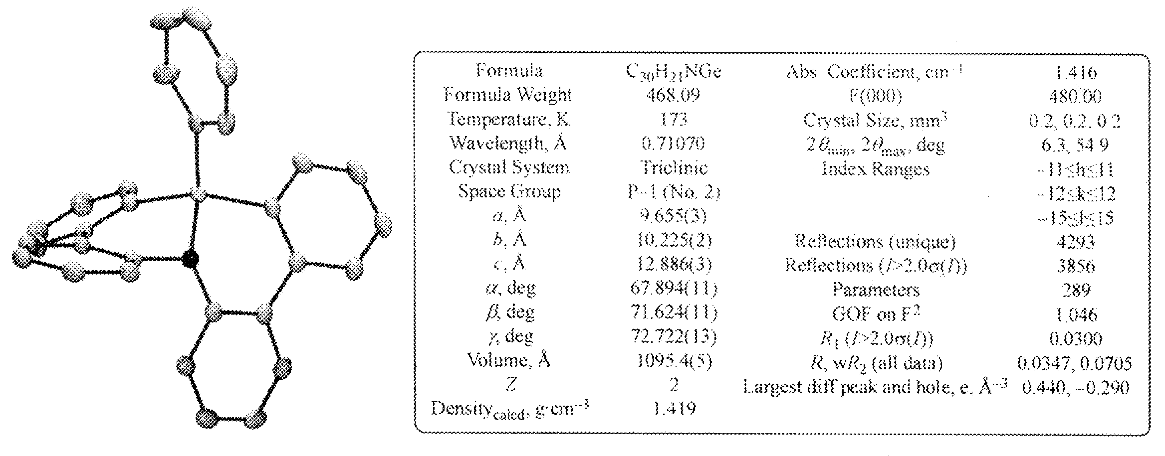
合成例1)

Anal. calcd for C24H16NB C, 87.56; H, 4.90; N, 4.25. found C, 87.79; H, 5.14; N, 4.31.
HRMS(EI) m/z; calcd. 329.1376[M]+; found 329.1380.
1H NMR (δppm in CS2/CD2Cl2=2/1, 600 MHz); 7.26-7.34 (m, 4H, NCCHCHCH), 7.55 (td, J = 1.2, 7.2 Hz, 2H, BCCHCH), 7.71 (td, J = 1.2, 7.2 Hz, 2H, BCCCHCH), 8.04 (dd, J = 1.8, 7.8 Hz, 2H, NCCH), 8.28 (dd, J = 1.8, 7.8 Hz, 2H, NCCCH), 8.33 (d, J = 7.8 Hz, 2H, BCCCH), 8.62 (dd, J = 1.2, 7.2 Hz, 2H, BCCH); 13C NMR (δppm in CS2/CD2Cl2=2/1, 151 MHz); 121.3 (2C), 123.1 (2C), 123.2 (2C), 125.6 (2C), 126.9 (4C), 127.6 (2C), 131.1 (2C), 132.6 (br, 2C, CBC), 135.6 (2C), 137.1 (2C), 138.8 (2C); 11B NMR (δppm in CS2/CD2Cl2=2/1, 193 MHz); 35.6;
合成例2)


Anal. calcd. for C24H14NBBr2 C, 59.19; H, 2.90; N, 2.88. found C, 59.13; H, 3.08; N, 2.93.
1H NMR (δppm in CDCl3, 392 MHz) 7.46 (dd, J = 2.3, 9.0 Hz, 2H, NCCHCH), 7.65 (t, J = 7.2 Hz, 2H, BCCHCH), 7.81 (t, J = 7.2 Hz, 2H, BCCHCHCH), 7.89 (d, J = 9.0 Hz, 2H, NCCH), 8.35 (d, J = 7.6 Hz, 2H, BCCCH), 8.46 (d, J = 2.3 Hz, 2H, NCCCH), 8.68 (d, J = 7.6 Hz, 2H, BCCH); 13C NMR (δppm in CDCl3, 98.5 MHz) ・・116.2 (2C), 122.8 (2C), 123.1 (2C), 127.6 (2C), 128.3 (2C), 129.5 (2C), 129.6 (2C), 131.5 (2C), 135.6 (2C), 135.7 (2C), 137.5 (2C).

HRMS(EI) m/z; calcd. 357.1689[M]+; found 357.1692.
11B NMR (δppm in C6D6) 34.0.

HRMS(EI) m/z; calcd. 327.1219[M]+; found 327.1215.
1H NMR (δppm in CDCl3); 7.66-7.72 (m, 4H), 7.84 (td, 2H, J = 1.4, 8.2 Hz), 8.21 (d, 2H, J = 7.8 Hz), 8.43 (d, 2H, J = 7.8 Hz), 8.67 (d, 2H, J = 7.8 Hz), 9.18 (d, 2H, J = 7.8 Hz).

HRMS(EI) m/z; calcd. 395.0440[M]+; found 395.0426.

HRMS(EI) m/z; calcd. 349.1020[M]+; found 349.1013.
31P NMR (δppm in C6D6) 12.7.

HRMS(ESI) m/z; calcd. 366.1042[M+H]+; found 366.1032.
31P NMR (δppm in C6D6) 6.6.

HRMS(FAB) m/z; calcd. 609.0778[M+H]+; found 609.0762.

Anal. calcd for C36H22N2B2C, 85.76; H, 4.40; N, 5.56. found C, 85.85; H, 4.24; N, 5.66.
1H NMR (δppm in CS2/CD2Cl2=2/1, 600 MHz) 7.31-7.34 (m, 4H, NCCCHCH), 7.55 (t, J = 8.4 Hz, 1H, NCCHCHCHCN), 7.61 (td, J = 1.2, 7.2 Hz, 2H, BCCHCHCHCH), 7.78 (td, J = 1.2, 7.2 Hz, 2H, BCCHCHCHCH), 7.91 (t, J = 7.2 Hz, 1H, BCCHCHCHCB), 8.05 (d, J = 8.4 Hz, 2H, NCCHCHCHCN), 8.11-8.13 (m, 2H, NCCHCHCHCH), 8.32-8.35 (m, 2H, NCCCH), 8.40 (d, J = 7.2 Hz, 2H, BCCCH), 8.71 (d, J = 7.2 Hz, 2H, BCCHCHCHCH), 8.96 (d, J = 7.2 Hz, 2H, BCCHCHCHCB); 13C NMR (δppm in CS2/CD2Cl2=2/1, 151 MHz) 114.3 (2C), 119.2, 121.8 (2C), 123.1 (2C), 123.4 (2C), 125.7, 125.8 (2C), 126.2, 126.7 (2C), 127.1 (2C), 128.1 (2C), 130.5 (br, 2C, CBCCCBC), 131.4 (2C), 133.0 (br, 2C, CBCCCBC), 135.8 (2C), 137.5 (4C), 137.6 (2C), 138.9, 139.0 (2C); 11B NMR (δppm in CS2/CD2Cl2=2/1, 193 MHz) 36.5.

HRMS(FAB) m/z; calcd. 580.2282[M]+; found 580.2296.
11B NMR (δppm in CS2/C6D6=2/1, 126 MHz) 35.7.

HRMS(EI) m/z; calcd. 335.0940[M]+; found 335.0926.
1H NMR (δppm in C6D6, 392 MHz) 6.92-7.11 (m, 5H), 7.39 (td, J = 0.9, 7.6 Hz, 1H), 7.50 (td, J = 1.8, 7.2 Hz, 1H), 7.91-8.00 (m, 4H), 8.11-8.16 (m, 2H), 8.63 (dd, J = 0.9, 7.6 Hz, 1H).
HRMS(EI) m/z; calcd. 335.0940[M]+; found 335.0943.
1H NMR (δppm in C6D6, 392 MHz) 7.00-7.05 (m, 2H), 7.07-7.12 (m, 2H), 7.40-7.50 (m, 3H), 7.63 (d, J = 4.9 Hz, 1H), 7.94 (dd, J = 1.8, 8.1 Hz, 1H), 8.03 (dd, J = 1.3, 8.5 Hz, 1H), 8.08-8.15 (m, 3H), 8.95 (dd, J = 1.4, 7.6 Hz, 1H).

HRMS(MALDI) m/z; calcd. 349.1091[M]+; found 349.1088.
11B NMR (δppm in C6D6, 126 MHz) 32.5.

HRMS(EI) m/z; calcd. 335.0940[M]+; found 335.0929.
11B NMR (δppm in C6D6, 126 MHz) 34.5.

HRMS(EI) m/z; calcd. 318.1328[M]+; found 318.1324.
1H NMR (δppm in C6D6, 392 MHz) 6.72-6.73 (m, 1H), 6.76-6.80 (m, 1H), 6.85-6.89 (m, 1H), 7.01-7.09 (m, 2H), 7.28 (dd, J = 1.3, 8.5 Hz, 1H), 7.35-7.39 (m, 1H), 7.46-7.51 (m, 2H), 7.55 (dd, J = 1.3, 3.6 Hz, 1H), 7.80 (dd, J = 1.3, 8.5 Hz, 1H), 7.86-7.89 (m, 1H), 8.09-8.13 (m, 2H), 8.71 (dd, J = 1.3, 7.6 Hz, 1H).


HRMS(EI) m/z; calcd. 429.1694[M]+; found 429.1698.
1H NMR (δppm in CDCl3); 6.65-6.69 (m, 2H), 7.11 (t, 2H, J = 7.4 Hz), 7.16 (d, 2H, J = 8.9 Hz), 7.64-7.70 (m, 4H), 7.79 (d, 2H, J = 8.9 Hz), 7.86 (dd, 2H, J = 0.9, 7.6 Hz), 8.48 (d, 2H, J = 8.9 Hz), 8.60 (d, 2H, J = 8.1 Hz), 8.84 (d, 2H, J = 7.1 Hz).

HRMS(EI) m/z; calcd. 379.1532[M]+; found 379.1521.
1H NMR (δppm in CDCl3); 7.04-7.06 (m, 2H), 7.10-7.15 (m, 1H), 7.18-7.22 (m, 1H), 7.37-7.41 (m, 1H), 7.58-7.62 (m, 2H), 7.63-7.67 (m, 1H), 7.77-7.89 (m, 4H), 8.30 (d, 1H, J = 7.6 Hz), 8.44 (d, 1H, J = 8.5 Hz), 8.46 (d, 1H, J = 8.0 Hz), 8.51 (d, 1H, J = 8.0 Hz), 8.74-8.77 (m, 2H).

HRMS(EI) m/z; calcd. 379.1532[M]+; found 379.1538.
1H NMR (δppm in CDCl3); 7.26-7.38 (m, 4H), 7.49-7.53 (m, 1H), 7.54-7.60 (m, 1H), 7.61-7.65 (m, 1H), 7.75-7.79 (m, 1H), 7.97-8.07 (m, 4H), 8.32 (dd, 1H, J = 1.6, 7.8 Hz), 8.38-8.43 (m, 2H), 8.73 (s, 1H), 8.78 (dd, 1H, J = 1.4, 7.6 Hz), 9.10 (s, 1H).

HRMS(EI) m/z; calcd. 586.9887[M]+; found 586.9885.
1H NMR (δppm in CDCl3); 6.79 (dt, 2H, J = 1.4, 7.7 Hz), 7.19-7.24 (m, 4H), 7.70 (t, 2H, J = 6.7 Hz), 7.90 (dt, 2H, J = 1.3, 7.4 Hz), 8.12 (d, 2H, J = 8.5 Hz), 8.55 (d, 2H, J = 8.1 Hz), 8.80 (s, 2H), 8.84 (d, 2H, J = 6.7 Hz).


1H NMR (δppm in CDCl3); 5.79 (s, 1H), 6.92 (t, J = 7.2 Hz, 2H), 7.17-7.27 (m, 14H), 7.40 (d, 2H, J = 8.1 Hz); 13C NMR (δppm in CDCl3) 117.0, 120.8, 127.2, 128.1, 128.7, 129.0, 130.6, 132.0, 138.9, 140.1.
26mm×28mm×0.5mmのガラス基板(日本板硝子(株)製)を透明支持基板とした。この透明支持基板を市販の蒸着装置の基板ホルダーに、2mm幅の下部アルミ電極を得るためのメタルマスクと同時に装着した。次いで、アルミニウムをのせたタングステン製の蒸着ボートを蒸着装置にセットした。
実施例29において用いた「4b-アザ-12b-ボラジベンゾ[g,p]クリセン」を「6c-アザ-16b-ボラジベンゾ[c,p]ナフト[1,2-g]クリセン」に変更し、蒸着した有機層の膜厚が8.2μmになった以外は同様の手法でサンプルを作製し、同様の方法で移動度の観測を行った。
Claims (10)
- 下記一般式(I)で表される部分構造を有する多環芳香族化合物又はその塩。

A環、B環、C環、D環は、同一又は異なって、置換されていてもよい芳香環又は置換されていてもよいヘテロ芳香環を示す。) - 下記一般式(II)で表される部分構造を有する、請求項1に記載の多環芳香族化合物又はその塩。

- 下記一般式(II-1)で表される部分構造を有する、請求項1に記載の多環芳香族化合物又はその塩。

- 下記一般式(II-2)~(II-54)のいずれかで表される部分構造を有する、請求項1に記載の多環芳香族化合物又はその塩。
 (式中、XはB、P、P=O、P=S、P=Se、As,As=O、As=S、As=Se、Sb、Sb=O、Sb=S、Sb=Se、または置換されていてもよい周期表第3~11族の金属、置換されていてもよい周期表第13~14族の金属又は半金属を示す。Zは、Se、S、O、またはN-を示す。)
- 下記一般式(II’)で表される請求項1に記載の多環芳香族化合物又はその塩。

- 下記一般式(II’-1)で表される請求項1に記載の多環芳香族化合物又はその塩。

- 下記一般式(III’)~(XXIII’)で表される請求項1に記載の多環芳香族化合物又はその塩。
 (式中、Yは、同一または異なってCRを表すか、Nを表すか、同じ環の隣接する2つのYは、各々それらの間の結合と一緒になってNR、O、SまたはSeを示す。XはB、P、P=O、P=S、P=Se、As,As=O、As=S、As=Se、Sb、Sb=O、Sb=S、Sb=Se、または置換されていてもよい周期表第3~11族の金属、置換されていてもよい周期表第13~14族の金属又は半金属を示す。Rは、水素原子、ハロゲン原子、C1-20アルキル基、ヒドロキシC1-20アルキル基、トリフルオロメチル基、C2-12パーフルオロアルキル基、C3-8シクロアルキル基、C2-20アルケニル基、C2-20アルキニル基、モノ若しくはジアリール置換アルケニル基、モノ若しくはジへテロアリール置換アルケニル基、アリールエチニル基、へテロアリールエチニル基、ヒドロキシ基、C1-20アルコキシ基、アリールオキシ基、トリフルオロメトキシ基、トリフルオロエトキシ基、C2-12パーフルオロアルコキシ基、C1-20アルキルカルボニル基、C1-20アルキルスルホニル基、シアノ基、ニトロ基、アミノ基、モノアルキルアミノ基、モノアリールアミノ基、モノヘテロアリールアミノ基、カルバゾール基、C1-20アルコキシカルボニルアミノ基、カルバモイル基、モノ若しくはジアルキルカルバモイル基、スルファモイル基、モノ若しくはジアルキルスルファモイル基、C1-20アルキルスルホニルアミノ基、C1-20アルキルカルボニルアミノ基、アリール基、ヘテロアリール基、C1-20アルコキシカルボニル基、カルボキシル基、5-テトラゾリル基、スルホ基(-SO2OH)又はフルオロスルホニル基、SRa、N(Ra)2、B(Ra)2、Si(Ra)3、-C≡C-Si(Ra)3(Raは置換されていてもよいアルキル基、置換されていてもよいアリール基または置換されていてもよいヘテロアリール基を示し、二つのRaはそれらが結合している原子と一緒になってヘテロ原子を有していてもよい二環式基または三環式基を示してもよい。)を意味し、ただし、アルキル基、アルケニル基、アルキニル基及びアルコキシ基は、ハロゲン原子、ヒドロキシ基、C1-20アルコキシ基、アリールオキシ基、アミノ基、カルバゾール基、N(Ra)2(Raは前記に定義されるとおりである)、トリフルオロメチル基、C2-12パーフルオロアルキル基、C3-8シクロアルキル基、アリール基及びヘテロアリール基から選択される1~3個の原子又は基で置換されていてもよく、かつ、上記アリール基、アリール部分、ヘテロアリール基、ヘテロアリール部分、カルバゾール基は、ハロゲン原子、C1-20アルキル基、ヒドロキシC1-20アルキル基、トリフルオロメチル基、C2-12パーフルオロアルキル基、C3-8シクロアルキル基、C2-20アルケニル基、C2-20アルキニル基、モノ若しくはジアリール置換アルケニル基、モノ若しくはジへテロアリール置換アルケニル基、アリールエチニル基、へテロアリールエチニル基、ヒドロキシ基、C1-20アルコキシ基、アリールオキシ基、トリフルオロメトキシ基、トリフルオロエトキシ基、C2-12パーフルオロアルコキシ基、シアノ基、ニトロ基、アミノ基、カルバゾール基、モノアルキルアミノ基、モノアリールアミノ基、モノヘテロアリールアミノ基、N(Ra)2(Raは前記に定義されるとおりである)、カルバモイル基、モノ若しくはジアルキルカルバモイル基、スルファモイル基、モノ若しくはジアルキルスルファモイル基、C1-20アルキルカルボニル基、C1-20アルキルスルホニル基、C1-20アルキルスルホニルアミノ基、C1-20アルキルカルボニルアミノ基、メチレンジオキシ基、ヘテロアリール基及びアリール基(当該アリール基は、ハロゲン原子、C1-20アルキル基、C3-8シクロアルキル基、C2-20アルケニル基、C2-20アルキニル基、ヒドロキシ基、トリフルオロメチル基、C2-12パーフルオロアルキル基、ヒドロキシ基、C1-20アルコキシ基、アリールオキシ基、トリフルオロメトキシ基、トリフルオロエトキシ基、C2-12パーフルオロアルコキシ基、C1-20アルキルカルボニル基、C1-20アルキルスルホニル基、メチレンジオキシ基、シアノ基、ニトロ基、アミノ基、カルバゾール基、N(Ra)2(Raは前記に定義されるとおりである)から選択される1~5個の原子又は基で置換されていてもよい)から選択される1~5個の原子又は基で置換されていてもよい。或いは、隣接する2つのR基は、これらが結合している炭素原子と一緒になって5員環又は6員環のヘテロ原子を有していてもよい単環式基、二環式基または三環式基を示し、隣接する3つのR基は、これらが結合している炭素原子と一緒になってヘテロ原子を有していてもよい二環式基または三環式基を示す。2つの隣接するR基が隣接する環のR基である場合、2つのR基は単結合、CH2、CHRa、CRa 2、NRa、Si(Ra)2、BRa(Raは前記に定義されるとおりである)、Se、S、またはOを示す。)
- 下記式(II’-1A)~(XIV’-1A)のいずれかで表される請求項1に記載の化合物。

 (式中、XはB、P、P=O、P=S、P=Se、As,As=O、As=S、As=Se、Sb、Sb=O、Sb=S、Sb=Se、または置換されていてもよい周期表第3~11族の金属、置換されていてもよい周期表第13~14族の金属又は半金属を示す。Rは、水素原子、ハロゲン原子、C1-20アルキル基、ヒドロキシC1-20アルキル基、トリフルオロメチル基、C2-12パーフルオロアルキル基、C3-8シクロアルキル基、C2-20アルケニル基、C2-20アルキニル基、モノ若しくはジアリール置換アルケニル基、モノ若しくはジへテロアリール置換アルケニル基、アリールエチニル基、へテロアリールエチニル基、ヒドロキシ基、C1-20アルコキシ基、アリールオキシ基、トリフルオロメトキシ基、トリフルオロエトキシ基、C2-12パーフルオロアルコキシ基、C1-20アルキルカルボニル基、C1-20アルキルスルホニル基、シアノ基、ニトロ基、アミノ基、モノアルキルアミノ基、モノアリールアミノ基、モノヘテロアリールアミノ基、カルバゾール基、C1-20アルコキシカルボニルアミノ基、カルバモイル基、モノ若しくはジアルキルカルバモイル基、スルファモイル基、モノ若しくはジアルキルスルファモイル基、C1-20アルキルスルホニルアミノ基、アリール基、ヘテロアリール基、C1-20アルコキシカルボニル基、カルボキシル基、5-テトラゾリル基、スルホ基(-SO2OH)又はフルオロスルホニル基、SRa、N(Ra)2、B(Ra)2、Si(Ra)3、-C≡C-Si(Ra)3(Raは置換されていてもよいアルキル基、置換されていてもよいアリール基または置換されていてもよいヘテロアリール基を示し、二つのRaはそれらが結合している原子と一緒になってヘテロ原子を有していてもよい二環式基または三環式基を示してもよい。)を意味し、ただし、アルキル基、アルケニル基、アルキニル基及びアルコキシ基は、ハロゲン原子、ヒドロキシ基、C1-20アルコキシ基、アリールオキシ基、アミノ基、カルバゾール基、N(Ra)2(Raは前記に定義されるとおりである)、トリフルオロメチル基、C2-12パーフルオロアルキル基、C3-8シクロアルキル基、アリール基及びヘテロアリール基から選択される1~3個の原子又は基で置換されていてもよく、かつ、上記アリール基、アリール部分、ヘテロアリール基、ヘテロアリール部分、カルバゾール基は、ハロゲン原子、C1-20アルキル基、ヒドロキシC1-20アルキル基、トリフルオロメチル基、C2-12パーフルオロアルキル基、C3-8シクロアルキル基、C2-20アルケニル基、C2-20アルキニル基、モノ若しくはジアリール置換アルケニル基、モノ若しくはジへテロアリール置換アルケニル基、アリールエチニル基、へテロアリールエチニル基、ヒドロキシ基、C1-20アルコキシ基、アリールオキシ基、トリフルオロメトキシ基、トリフルオロエトキシ基、C2-12パーフルオロアルコキシ基、シアノ基、ニトロ基、アミノ基、カルバゾール基、モノアルキルアミノ基、モノアリールアミノ基、モノヘテロアリールアミノ基、N(Ra)2(Raは前記に定義されるとおりである)、カルバモイル基、モノ若しくはジアルキルカルバモイル基、スルファモイル基、モノ若しくはジアルキルスルファモイル基、C1-20アルキルカルボニル基、C1-20アルキルスルホニル基、C1-20アルキルスルホニルアミノ基、C1-20アルキルカルボニルアミノ基、メチレンジオキシ基、ヘテロアリール基及びアリール基(当該アリール基は、ハロゲン原子、C1-20アルキル基、C3-8シクロアルキル基、C2-20アルケニル基、C2-20アルキニル基、ヒドロキシ基、トリフルオロメチル基、C2-12パーフルオロアルキル基、ヒドロキシ基、C1-20アルコキシ基、アリールオキシ基、トリフルオロメトキシ基、トリフルオロエトキシ基、C2-12パーフルオロアルコキシ基、C1-20アルキルカルボニル基、C1-20アルキルスルホニル基、メチレンジオキシ基、シアノ基、ニトロ基、アミノ基、カルバゾール基、N(Ra)2(Raは前記に定義されるとおりである)から選択される1~5個の原子又は基で置換されていてもよい)から選択される1~5個の原子又は基で置換されていてもよい。或いは、隣接する2つのR基は、これらが結合している炭素原子と一緒になって5員環又は6員環のヘテロ原子を有していてもよい単環式基、二環式基または三環式基を示し、隣接する3つのR基は、これらが結合している炭素原子と一緒になってヘテロ原子を有していてもよい二環式基または三環式基を示す。2つの隣接するR基が隣接する環のR基である場合、2つのR基は単結合、CH2、CHRa、CRa 2、NRa、Si(Ra)2、BRa(Raは前記に定義されるとおりである)、Se、S、またはOを示す。)
- 請求項1~8のいずれかに記載の化合物を含む、電気化学デバイス。
- 有機発光素子、有機薄膜トランジスタまたは有機薄膜太陽電池である請求項9に記載の電気化学デバイス。
Priority Applications (7)
| Application Number | Priority Date | Filing Date | Title |
|---|---|---|---|
| JP2013503640A JP5744176B2 (ja) | 2011-03-10 | 2012-03-09 | 多環芳香族化合物 |
| EP12755603.3A EP2752418B1 (en) | 2011-03-10 | 2012-03-09 | Polycyclic aromatic compound |
| EP17178054.7A EP3260458B1 (en) | 2011-03-10 | 2012-03-09 | Polycyclic aromatic compound |
| KR1020137024502A KR101757155B1 (ko) | 2011-03-10 | 2012-03-09 | 다중고리 방향족 화합물 |
| US14/003,945 US9166176B2 (en) | 2011-03-10 | 2012-03-09 | Polycyclic aromatic compound |
| CN201280012314.2A CN103429599B (zh) | 2011-03-10 | 2012-03-09 | 多环芳香族化合物 |
| US14/832,414 US9741950B2 (en) | 2011-03-10 | 2015-08-21 | Polycyclic aromatic compound |
Applications Claiming Priority (2)
| Application Number | Priority Date | Filing Date | Title |
|---|---|---|---|
| JP2011-053242 | 2011-03-10 | ||
| JP2011053242 | 2011-03-10 |
Related Child Applications (2)
| Application Number | Title | Priority Date | Filing Date |
|---|---|---|---|
| US14/003,945 A-371-Of-International US9166176B2 (en) | 2011-03-10 | 2012-03-09 | Polycyclic aromatic compound |
| US14/832,414 Division US9741950B2 (en) | 2011-03-10 | 2015-08-21 | Polycyclic aromatic compound |
Publications (1)
| Publication Number | Publication Date |
|---|---|
| WO2012121398A1 true WO2012121398A1 (ja) | 2012-09-13 |
Family
ID=46798349
Family Applications (1)
| Application Number | Title | Priority Date | Filing Date |
|---|---|---|---|
| PCT/JP2012/056206 WO2012121398A1 (ja) | 2011-03-10 | 2012-03-09 | 多環芳香族化合物 |
Country Status (6)
| Country | Link |
|---|---|
| US (2) | US9166176B2 (ja) |
| EP (2) | EP3260458B1 (ja) |
| JP (1) | JP5744176B2 (ja) |
| KR (1) | KR101757155B1 (ja) |
| CN (1) | CN103429599B (ja) |
| WO (1) | WO2012121398A1 (ja) |
Cited By (12)
| Publication number | Priority date | Publication date | Assignee | Title |
|---|---|---|---|---|
| JP2014024845A (ja) * | 2012-07-30 | 2014-02-06 | Universal Display Corp | ホウ素−窒素多環芳香族化合物及びoledにおけるそれらの使用 |
| WO2014042197A1 (ja) * | 2012-09-11 | 2014-03-20 | Jnc株式会社 | 有機電界発光素子用材料、有機電界発光素子、表示装置、及び照明装置 |
| WO2015043722A1 (en) * | 2013-09-30 | 2015-04-02 | Merck Patent Gmbh | Azaborinine derivatives, their synthesis and use in organic electronic devices |
| WO2016143624A1 (ja) * | 2015-03-09 | 2016-09-15 | 学校法人関西学院 | 多環芳香族化合物および発光層形成用組成物 |
| CN106986894A (zh) * | 2016-01-20 | 2017-07-28 | 中国科学院宁波材料技术与工程研究所 | 硫、磷杂原子取代二苯并[g,p]稠二萘型衍生物、其制备方法与应用 |
| US10033004B2 (en) | 2015-06-01 | 2018-07-24 | Universal Display Corporation | Organic electroluminescent materials and devices |
| JP2018125387A (ja) * | 2017-01-31 | 2018-08-09 | 日本放送協会 | 有機エレクトロルミネッセンス素子 |
| US10418568B2 (en) | 2015-06-01 | 2019-09-17 | Universal Display Corporation | Organic electroluminescent materials and devices |
| US10468609B2 (en) | 2016-06-02 | 2019-11-05 | Universal Display Corporation | Organic electroluminescent materials and devices |
| WO2020094542A1 (de) | 2018-11-06 | 2020-05-14 | Merck Patent Gmbh | 5,6-diphenyl-5,6-dihydro-dibenz[c,e][1,2]azaphosphorin- und 6-phenyl-6h-dibenzo[c,e][1,2]thiazin-5,5-dioxid-derivate und ähnliche verbindungen als organische elektrolumineszenzmaterialien für oleds |
| US11056656B2 (en) | 2017-05-11 | 2021-07-06 | Merck Patent Gmbh | Organoboron complexes and their use in organic electroluminescent devices |
| US11731990B2 (en) | 2017-05-11 | 2023-08-22 | Merck Patent Gmbh | Carbazole-based Bodipys for organic electroluminescent devices |
Families Citing this family (16)
| Publication number | Priority date | Publication date | Assignee | Title |
|---|---|---|---|---|
| WO2012121398A1 (ja) * | 2011-03-10 | 2012-09-13 | 国立大学法人京都大学 | 多環芳香族化合物 |
| CN104098597B (zh) * | 2014-07-08 | 2016-08-24 | 同济大学 | 一种合成4a,8a-硼氮杂萘及其衍生物的方法 |
| US9871212B2 (en) * | 2014-11-14 | 2018-01-16 | Universal Display Corporation | Organic electroluminescent materials and devices |
| US9882151B2 (en) | 2014-11-14 | 2018-01-30 | Universal Display Corporation | Organic electroluminescent materials and devices |
| WO2016116520A1 (de) * | 2015-01-20 | 2016-07-28 | Cynora Gmbh | Phenylether-substituierte organische moleküle, insbesondere zur verwendung in optoelektronischen bauelementen |
| KR102384779B1 (ko) | 2016-09-07 | 2022-04-08 | 가꼬우 호징 관세이 가쿠잉 | 다환 방향족 화합물 |
| JP7030302B2 (ja) * | 2016-10-28 | 2022-03-07 | 学校法人関西学院 | ボロン酸またはボロン酸エステル、もしくはそれらを用いて多環芳香族化合物または多環芳香族多量体化合物を製造する方法 |
| US10998506B2 (en) | 2017-08-22 | 2021-05-04 | Beijing Summer Sprout Technology Co., Ltd. | Boron containing heterocyclic compound for OLEDs, an organic light-emitting device, and a formulation comprising the boron-containing heterocyclic compound |
| CN108503657B (zh) * | 2017-12-20 | 2022-08-16 | 天津理工大学 | 含五元杂环的硼氮掺杂稠环芳香烃及其合成方法及应用 |
| CN108299481B (zh) * | 2018-01-12 | 2020-10-09 | 华南协同创新研究院 | 电致发光聚合单体、聚合物及其制备方法和应用 |
| JP7039414B2 (ja) * | 2018-07-26 | 2022-03-22 | 株式会社東芝 | 放射線検出素子の作製方法および放射線検出素子 |
| CN110776524B (zh) * | 2018-07-31 | 2021-09-21 | 华南理工大学 | 一类含硼氮基团的吡啶并二唑衍生物及其制备方法与应用 |
| US20230010535A1 (en) * | 2019-12-20 | 2023-01-12 | Dupont Electronics, Inc. | Electroactive compounds |
| KR20210083464A (ko) * | 2019-12-26 | 2021-07-07 | 삼성디스플레이 주식회사 | 유기 전계 발광 소자 및 유기 전계 발광 소자용 다환 화합물 |
| CN113980055B (zh) * | 2021-11-26 | 2023-09-29 | 南阳师范学院 | 具联芳骨架的环状膦酰胺类衍生物、合成方法及应用 |
| CN114957303A (zh) * | 2022-05-12 | 2022-08-30 | 天津理工大学 | 一种嵌有吲哚单元的硼氮掺杂多环共轭芳烃及其合成方法和应用 |
Citations (4)
| Publication number | Priority date | Publication date | Assignee | Title |
|---|---|---|---|---|
| JP2006004721A (ja) | 2004-06-16 | 2006-01-05 | Fuji Electric Holdings Co Ltd | トップエミッション型有機el素子 |
| JP2007027141A (ja) | 2001-12-05 | 2007-02-01 | Semiconductor Energy Lab Co Ltd | 有機半導体素子の作製方法 |
| JP2008171832A (ja) | 2001-12-05 | 2008-07-24 | Semiconductor Energy Lab Co Ltd | 有機エレクトロルミネッセンス素子の作製方法 |
| WO2010053818A2 (en) | 2008-11-10 | 2010-05-14 | Schlumberger Canada Limited | Gain stabilization of gamma-ray scintillation detector |
Family Cites Families (2)
| Publication number | Priority date | Publication date | Assignee | Title |
|---|---|---|---|---|
| JP5615261B2 (ja) * | 2009-03-11 | 2014-10-29 | 学校法人関西学院 | 多環芳香族化合物 |
| WO2012121398A1 (ja) * | 2011-03-10 | 2012-09-13 | 国立大学法人京都大学 | 多環芳香族化合物 |
-
2012
- 2012-03-09 WO PCT/JP2012/056206 patent/WO2012121398A1/ja active Application Filing
- 2012-03-09 KR KR1020137024502A patent/KR101757155B1/ko active IP Right Grant
- 2012-03-09 EP EP17178054.7A patent/EP3260458B1/en active Active
- 2012-03-09 US US14/003,945 patent/US9166176B2/en active Active
- 2012-03-09 CN CN201280012314.2A patent/CN103429599B/zh active Active
- 2012-03-09 JP JP2013503640A patent/JP5744176B2/ja active Active
- 2012-03-09 EP EP12755603.3A patent/EP2752418B1/en active Active
-
2015
- 2015-08-21 US US14/832,414 patent/US9741950B2/en active Active
Patent Citations (4)
| Publication number | Priority date | Publication date | Assignee | Title |
|---|---|---|---|---|
| JP2007027141A (ja) | 2001-12-05 | 2007-02-01 | Semiconductor Energy Lab Co Ltd | 有機半導体素子の作製方法 |
| JP2008171832A (ja) | 2001-12-05 | 2008-07-24 | Semiconductor Energy Lab Co Ltd | 有機エレクトロルミネッセンス素子の作製方法 |
| JP2006004721A (ja) | 2004-06-16 | 2006-01-05 | Fuji Electric Holdings Co Ltd | トップエミッション型有機el素子 |
| WO2010053818A2 (en) | 2008-11-10 | 2010-05-14 | Schlumberger Canada Limited | Gain stabilization of gamma-ray scintillation detector |
Non-Patent Citations (5)
| Title |
|---|
| "Organic electroluminescence materials and displays", CMC CO., LTD., pages: 69 - 70 |
| JIN QIANG HOU ET AL., THE JOURNAL OF PHYSICAL CHEMISTRY A, vol. 111, 2007, pages 1111 - 1116, XP055128010 * |
| MARIA S. MUDADU ET AL., THE JOURNAL OT ORGANIC CHEMISTRY, vol. 73, 2008, pages 6513 - 6520, XP055128047 * |
| See also references of EP2752418A4 |
| TAKUJI HATAKEYAMA ET AL., JOURNAL OF THE AMERICAN CHEMICAL SOCIETY, vol. 133, 25 October 2011 (2011-10-25), pages 18614 - 18617, XP055128034 * |
Cited By (23)
| Publication number | Priority date | Publication date | Assignee | Title |
|---|---|---|---|---|
| US9627631B2 (en) | 2012-07-30 | 2017-04-18 | Universal Display Corporation | Organic electroluminescent materials and devices |
| JP2017206541A (ja) * | 2012-07-30 | 2017-11-24 | ユニバーサル ディスプレイ コーポレイション | ホウ素−窒素多環芳香族化合物及びoledにおけるそれらの使用 |
| JP2014024845A (ja) * | 2012-07-30 | 2014-02-06 | Universal Display Corp | ホウ素−窒素多環芳香族化合物及びoledにおけるそれらの使用 |
| CN107266481A (zh) * | 2012-09-11 | 2017-10-20 | 捷恩智株式会社 | 有机电场发光元件用材料、有机电场发光元件、显示装置、以及照明装置 |
| TWI612054B (zh) * | 2012-09-11 | 2018-01-21 | 捷恩智股份有限公司 | 有機電場發光元件、顯示裝置以及照明裝置 |
| JP2015216380A (ja) * | 2012-09-11 | 2015-12-03 | Jnc株式会社 | 有機電界発光素子用材料、有機電界発光素子、表示装置、及び照明装置 |
| JP2015188099A (ja) * | 2012-09-11 | 2015-10-29 | Jnc株式会社 | 有機電界発光素子用材料、有機電界発光素子、表示装置、及び照明装置 |
| CN107266481B (zh) * | 2012-09-11 | 2020-04-14 | 捷恩智株式会社 | 有机电场发光元件用材料、有机电场发光元件、显示装置、以及照明装置 |
| WO2014042197A1 (ja) * | 2012-09-11 | 2014-03-20 | Jnc株式会社 | 有機電界発光素子用材料、有機電界発光素子、表示装置、及び照明装置 |
| JP5819534B2 (ja) * | 2012-09-11 | 2015-11-24 | Jnc株式会社 | 有機電界発光素子用材料、有機電界発光素子、表示装置、及び照明装置 |
| CN105814066A (zh) * | 2013-09-30 | 2016-07-27 | 默克专利股份有限公司 | 氮杂硼杂苯衍生物,它们的合成及其在有机电子器件中的用途 |
| US10840460B2 (en) | 2013-09-30 | 2020-11-17 | Flexenable Limited | Azaborinine derivatives, their synthesis and use in organic electronic devices |
| WO2015043722A1 (en) * | 2013-09-30 | 2015-04-02 | Merck Patent Gmbh | Azaborinine derivatives, their synthesis and use in organic electronic devices |
| JPWO2016143624A1 (ja) * | 2015-03-09 | 2017-12-21 | 学校法人関西学院 | 多環芳香族化合物および発光層形成用組成物 |
| WO2016143624A1 (ja) * | 2015-03-09 | 2016-09-15 | 学校法人関西学院 | 多環芳香族化合物および発光層形成用組成物 |
| US10033004B2 (en) | 2015-06-01 | 2018-07-24 | Universal Display Corporation | Organic electroluminescent materials and devices |
| US10418568B2 (en) | 2015-06-01 | 2019-09-17 | Universal Display Corporation | Organic electroluminescent materials and devices |
| CN106986894A (zh) * | 2016-01-20 | 2017-07-28 | 中国科学院宁波材料技术与工程研究所 | 硫、磷杂原子取代二苯并[g,p]稠二萘型衍生物、其制备方法与应用 |
| US10468609B2 (en) | 2016-06-02 | 2019-11-05 | Universal Display Corporation | Organic electroluminescent materials and devices |
| JP2018125387A (ja) * | 2017-01-31 | 2018-08-09 | 日本放送協会 | 有機エレクトロルミネッセンス素子 |
| US11056656B2 (en) | 2017-05-11 | 2021-07-06 | Merck Patent Gmbh | Organoboron complexes and their use in organic electroluminescent devices |
| US11731990B2 (en) | 2017-05-11 | 2023-08-22 | Merck Patent Gmbh | Carbazole-based Bodipys for organic electroluminescent devices |
| WO2020094542A1 (de) | 2018-11-06 | 2020-05-14 | Merck Patent Gmbh | 5,6-diphenyl-5,6-dihydro-dibenz[c,e][1,2]azaphosphorin- und 6-phenyl-6h-dibenzo[c,e][1,2]thiazin-5,5-dioxid-derivate und ähnliche verbindungen als organische elektrolumineszenzmaterialien für oleds |
Also Published As
| Publication number | Publication date |
|---|---|
| KR101757155B1 (ko) | 2017-07-12 |
| US20160049600A1 (en) | 2016-02-18 |
| US9166176B2 (en) | 2015-10-20 |
| US9741950B2 (en) | 2017-08-22 |
| CN103429599A (zh) | 2013-12-04 |
| EP2752418A1 (en) | 2014-07-09 |
| EP3260458A1 (en) | 2017-12-27 |
| CN103429599B (zh) | 2016-09-07 |
| JPWO2012121398A1 (ja) | 2014-07-17 |
| EP2752418B1 (en) | 2017-11-29 |
| EP3260458B1 (en) | 2019-09-18 |
| JP5744176B2 (ja) | 2015-07-01 |
| EP2752418A4 (en) | 2014-09-10 |
| KR20140008395A (ko) | 2014-01-21 |
| US20140005399A1 (en) | 2014-01-02 |
Similar Documents
| Publication | Publication Date | Title |
|---|---|---|
| JP5744176B2 (ja) | 多環芳香族化合物 | |
| EP2871222B1 (en) | Compound for organic optoelectric device, organic optoelectric device comprising same, and display apparatus comprising organic optoelectric device | |
| JP6538504B2 (ja) | 有機金属錯体、発光素子、発光装置、電子機器、及び照明装置 | |
| KR102402723B1 (ko) | 스피로바이플루오렌-구조를 갖는 화합물 | |
| CN106543149B (zh) | 化合物和包括该化合物的有机发光装置 | |
| KR102626926B1 (ko) | 유기금속 화합물 및 이를 포함한 유기 발광 소자 | |
| TWI588150B (zh) | 雜環化合物及其利用 | |
| KR20160109907A (ko) | 유기금속 화합물 및 이를 포함한 유기 발광 소자 | |
| US20120048377A1 (en) | Photosensitive optoelectronic devices comprising polycyclic aromatic compounds | |
| JP6449434B2 (ja) | ヘテロ環化合物又はその塩、及びこれらを含む電子デバイス | |
| WO2014157618A1 (ja) | 有機エレクトロルミネッセンス素子、それを具備した照明装置及び表示装置 | |
| JP7445927B2 (ja) | 多環芳香族化合物 | |
| TW202039417A (zh) | 電子裝置之材料 | |
| KR20210044175A (ko) | 다환 고리 화합물 및 이를 이용한 유기발광소자 | |
| KR102637099B1 (ko) | 유기금속 화합물 및 이를 포함한 유기 발광 소자 | |
| CN106749050B (zh) | 一种以环状二酮为核心的热激活延迟荧光oled材料及其应用 | |
| JP7450342B2 (ja) | 有機金属化合物とそれを含む有機発光素子及び診断用組成物 | |
| JP6641947B2 (ja) | 有機エレクトロルミネッセンス素子、表示装置、照明装置及び芳香族複素環誘導体 | |
| JP6641948B2 (ja) | 有機エレクトロルミネッセンス素子、表示装置、照明装置及び芳香族複素環誘導体 | |
| KR101739831B1 (ko) | 유기 발광 화합물, 잉크 조성물, 유기 발광 소자 및 전자 기기 | |
| TWI827776B (zh) | 有機金屬化合物和包括其的有機發光器件 | |
| KR20190118821A (ko) | 축합환 화합물 및 이를 포함한 유기 발광 소자 | |
| KR20230151470A (ko) | 유기 전계발광재료 및 그 소자 | |
| KR20230140417A (ko) | 유기 전계발광재료 및 그 소자 | |
| KR20240028316A (ko) | 유기 전계발광재료 및 그 소자 |
Legal Events
| Date | Code | Title | Description |
|---|---|---|---|
| 121 | Ep: the epo has been informed by wipo that ep was designated in this application |
Ref document number: 12755603 Country of ref document: EP Kind code of ref document: A1 |
|
| ENP | Entry into the national phase |
Ref document number: 2013503640 Country of ref document: JP Kind code of ref document: A |
|
| NENP | Non-entry into the national phase |
Ref country code: DE |
|
| ENP | Entry into the national phase |
Ref document number: 20137024502 Country of ref document: KR Kind code of ref document: A |
|
| WWE | Wipo information: entry into national phase |
Ref document number: 14003945 Country of ref document: US |
|
| REEP | Request for entry into the european phase |
Ref document number: 2012755603 Country of ref document: EP |
|
| WWE | Wipo information: entry into national phase |
Ref document number: 2012755603 Country of ref document: EP |