US9576646B2 - SRAM cell with dynamic split ground and split wordline - Google Patents
SRAM cell with dynamic split ground and split wordline Download PDFInfo
- Publication number
- US9576646B2 US9576646B2 US14/963,586 US201514963586A US9576646B2 US 9576646 B2 US9576646 B2 US 9576646B2 US 201514963586 A US201514963586 A US 201514963586A US 9576646 B2 US9576646 B2 US 9576646B2
- Authority
- US
- United States
- Prior art keywords
- gndl
- gndr
- inverter
- memory cell
- vdd
- Prior art date
- Legal status (The legal status is an assumption and is not a legal conclusion. Google has not performed a legal analysis and makes no representation as to the accuracy of the status listed.)
- Expired - Fee Related
Links
Images


Classifications
-
- G—PHYSICS
- G11—INFORMATION STORAGE
- G11C—STATIC STORES
- G11C11/00—Digital stores characterised by the use of particular electric or magnetic storage elements; Storage elements therefor
- G11C11/21—Digital stores characterised by the use of particular electric or magnetic storage elements; Storage elements therefor using electric elements
- G11C11/34—Digital stores characterised by the use of particular electric or magnetic storage elements; Storage elements therefor using electric elements using semiconductor devices
- G11C11/40—Digital stores characterised by the use of particular electric or magnetic storage elements; Storage elements therefor using electric elements using semiconductor devices using transistors
- G11C11/41—Digital stores characterised by the use of particular electric or magnetic storage elements; Storage elements therefor using electric elements using semiconductor devices using transistors forming static cells with positive feedback, i.e. cells not needing refreshing or charge regeneration, e.g. bistable multivibrator or Schmitt trigger
- G11C11/413—Auxiliary circuits, e.g. for addressing, decoding, driving, writing, sensing, timing or power reduction
- G11C11/417—Auxiliary circuits, e.g. for addressing, decoding, driving, writing, sensing, timing or power reduction for memory cells of the field-effect type
- G11C11/419—Read-write [R-W] circuits
-
- G—PHYSICS
- G11—INFORMATION STORAGE
- G11C—STATIC STORES
- G11C11/00—Digital stores characterised by the use of particular electric or magnetic storage elements; Storage elements therefor
- G11C11/21—Digital stores characterised by the use of particular electric or magnetic storage elements; Storage elements therefor using electric elements
- G11C11/34—Digital stores characterised by the use of particular electric or magnetic storage elements; Storage elements therefor using electric elements using semiconductor devices
- G11C11/40—Digital stores characterised by the use of particular electric or magnetic storage elements; Storage elements therefor using electric elements using semiconductor devices using transistors
- G11C11/41—Digital stores characterised by the use of particular electric or magnetic storage elements; Storage elements therefor using electric elements using semiconductor devices using transistors forming static cells with positive feedback, i.e. cells not needing refreshing or charge regeneration, e.g. bistable multivibrator or Schmitt trigger
- G11C11/413—Auxiliary circuits, e.g. for addressing, decoding, driving, writing, sensing, timing or power reduction
- G11C11/417—Auxiliary circuits, e.g. for addressing, decoding, driving, writing, sensing, timing or power reduction for memory cells of the field-effect type
- G11C11/418—Address circuits
-
- G—PHYSICS
- G11—INFORMATION STORAGE
- G11C—STATIC STORES
- G11C8/00—Arrangements for selecting an address in a digital store
- G11C8/14—Word line organisation; Word line lay-out
Definitions
- the invention relates to semiconductor structures and, more particularly, to an SRAM cell with dynamic split ground (GND) and split wordline (WL) for extreme scaling.
- GND dynamic split ground
- WL split wordline
- SRAM Static Random Access Memory
- Various methods have been employed to maintain stability but generally at the cost of performance, density and design assist overhead.
- one approach is to use asymmetric SRAM cells to improve stability with one-sided sensing.
- the wordline is split into a wordline left (WL) and a wordline right (WR).
- the SRAM can be read on one side only with either the WR or the WL. In this way, during read operation only the word line of the sensing side is activated.
- the SRAM cell is not useful for differential sensing. That is, the SRAM cell is not useful for SRAM designs with standard differential sensing from a bitline left (BL) and a bitline right (BR).
- Asymmetric designs also impose undesirable constraints on the SRAM applications. For example, the bit line on one side cannot be used as a 2nd read port. This effectively slows down the read/write operations. Also, the SRAM cell cannot serves as standard cell type where the asymmetric stability is not needed. Power down scheme in low power applications gets more complicated or compromised.
- a memory cell comprises a first access transistor enabled by a first wordline to control access to cross coupled inverters by a first bitline.
- the memory cell further comprises a second access transistor enabled by a second wordline to control access to the cross coupled inverters by a second bitline.
- the memory cell further comprises a split ground line comprising a first ground line (GNDL) separated from a second ground line (GNDR).
- GNDL is connected to a transistor of a first inverter of the cross coupled inverters and the GNDR is connected to a first transistor of a second inverter of the cross coupled inverters.
- a memory cell comprises: cross coupled inverters comprising PFETs and NFETs; a bitline left (BL) which accesses a first inverter of cross coupled inverters by enabling a first access transistor; a bitline right (BR) which accesses a second inverter of the cross coupled inverters by enabling a second access transistor; a wordline left (WL) with enables the first access transistor; a wordline right (WR) which enables the second access transistor; and a split vertical ground line comprising a first vertical ground line (GNDL) separated from a second vertical ground line (GNDR), the GNDL is connected to the first inverter of the cross coupled inverters and the GNDR is connected to the second inverter of the cross coupled inverters.
- BL bitline left
- BR bitline right
- GNDL vertical ground line
- GNDR vertical ground line
- read operation of a memory cell comprises enabling a first transistor of an asymmetric memory cell to allow access of a first bitline to a storage cell, while raising or lowering a vertical ground line of two separated ground lines connected to transistors of the storage cell above or below ground, GND.
- FIG. 1 shows an SRAM cell in accordance with aspects of the present invention
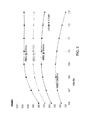
- FIG. 2 shows a performance graph comparing the SRAM cell designs of the present invention to a conventional asymmetric SRAM
- FIG. 3 shows a table of extended exploitation of split GND for SRAM scaling
- FIG. 4 shows the impact of the SRAM cell design of the present invention to data retention margins (DRM).
- the invention relates to semiconductor structures and, more particularly, to an SRAM cell with dynamic split ground (GND) and split wordline (WL) for extreme scaling.
- the SRAM cell design includes separate vertical SRAM GND buses, e.g., GND left (GNDL) and GND right (GNDR).
- GND left (GNDL) and GND right (GNDR) are separate vertical SRAM GND buses, e.g., GND left (GNDL) and GND right (GNDR).
- GNDL GND left
- GNDR GND right
- the SRAM cell of the present invention thus provides increased stability gain for asymmetric devices, while also allowing for differential sensing.
- GNDL and GNDR can be dynamically shifted to enhance stability of the asymmetric device, depending on the read side of the cell.
- GNDL can be shifted upwards, e.g., increase voltage above GND, while the sensing is on bitline right (BR); whereas, GNDR can be shifted upwards, e.g., increase voltage above GND, while sensing is on the bitline left (BL).
- both BL and BR can serve for 1-sided sensing, besides serving for more effective write operation.
- Extended enhancement on writability and power/performance also becomes available with different GND shift patterns, implemented with the SRAM cell design of the present invention.
- SRAM with fast NFET for quick access or with high bit line loading for array layout efficiency stability is enhanced with dynamic split GND.
- the SRAM cells of the present invention can be manufactured in a number of ways using a number of different tools.
- the methodologies and tools are used to form structures with dimensions in the micrometer and nanometer scale.
- the methodologies, i.e., technologies, employed to manufacture the SRAM cells of the present invention have been adopted from integrated circuit (IC) technology.
- IC integrated circuit
- the structures of the present invention are built on wafers and are realized in films of material patterned by photolithographic processes on the top of a wafer.
- the fabrication of the SRAM cells of the present invention uses three basic building blocks: (i) deposition of thin films of material on a substrate, (ii) applying a patterned mask on top of the films by photolithographic imaging, and (iii) etching the films selectively to the mask.
- FIG. 1 shows an asymmetric SRAM cell in accordance with aspects of the present invention.
- the asymmetric SRAM cell 10 includes a bitline right BR and bitline left BL, in addition to a wordline right WR and a wordline left WL.
- the asymmetric SRAM 10 further includes two cross-coupled inverters 15 , comprising four transistors P 0 , P 1 , N 0 and N 1 ; although more transistors per bit for multi-port applications are also contemplated by the present invention.
- the transistors P 0 , P 1 are PFETs and the transistors N 0 , N 1 are NFETs.
- the asymmetric SRAM 10 further includes access transistors T 0 and T 1 .
- the access transistors T 0 and T 1 serve to control the access to the storage cell, e.g., cross-coupled inverters 15 , during read and write operations.
- access to the storage cell 15 is enabled by the word lines WL and/or WR, which controls the respective access transistors T 0 and T 1 which, in turn, control whether the storage cell 15 should be connected to (e.g., accessed by) the respective bit lines BL and BR.
- the access transistors T 0 and T 1 are used to transfer data for both read and write operations.
- CL is the node across T 0 from BL and CR is the node across T 1 from BR.
- the GNDL is raised to Vdd to pull down CR and push up CL.
- the GNDR is raised to Vdd to pull down the CL and push up the CR.
- the GNDL of specific columns are raised to Vdd, and the GNDR of other specific columns are raised to Vdd.
- the asymmetric SRAM 10 further includes a vertical split ground line, e.g., GNDL and GNDR.
- the ground line GNDL is connected directly to transistor N 0 on the left side of the asymmetric SRAM 10 ; that is, the ground line GNDL is isolated from transistor N 1 on the right side of the asymmetric SRAM 10 .
- the ground line GNDR is connected directly to transistor N 1 on the right side of the asymmetric SRAM 10 ; that is, the ground line GNDR is isolated from transistor N 0 on the left side of the asymmetric SRAM 10 .
- the vertical GND lines (GNDR and GNDL) are kept separate; instead of being strapped together as in conventional SRAM cells.
- the SRAM cell 10 has three different operating modes or states: standby mode, reading mode and writing mode. In standby mode, the SRAM cell 10 is idle; whereas, in reading mode, the data are read out and in writing mode, the contents of the cell are updated.
- standby mode the SRAM cell 10 is idle; whereas, in reading mode, the data are read out and in writing mode, the contents of the cell are updated.
- the SRAM cell 10 of the present invention provides the necessary “stability” and “write-ability” which had been diminishing in conventional SRAM cells of scaled down dimensions.
- the wordline WL is raised to bring down the bitline BL for sensing.
- the GNDL is lowered by about 10% of Vdd below common ground, GND.
- GNDR can be simultaneously raised above common ground GND by about 10% of Vdd to minimize read disturb.
- the wordline WR is raised to bring down the bitline BR.
- GNDR is lowered below common GND to help sensing.
- the GNDL can be simultaneously raised by about 10% of Vdd above common GND to minimize read disturb.
- FIG. 2 shows a graph of stability of the SRAM cell designs with a shift of GNDL.
- the y-axis represents sigma (of Access Disturb Margin (ADM)) and the x-axis is supply voltage.
- ADM Access Disturb Margin
- the sigma is about 4.0, which is below the required stability at 6.0 ⁇ (sigma) for a possible failure rate around 1 part per billion.
- FIG. 3 shows a table of extended exploitation of split GND for SRAM scaling.
- the split GND design of the present invention provides very efficient write assist when the cell GNDL or GNDR is elevated above the bit line down level 0 (referred as elevated GND assist).
- elevated GND assist the standby cell Vdd is at an elevated GND (e.g., GNDH).
- GNDH is elevated to about 10-15% of Vdd above GND.
- stability assist and write assist are provided with small voltage shift of GNDL or GNDR relative to common GND.
- Write0 refers to pulling down CR and pushing up CL, where CR is the cell node on the right side and CL is the cell node on the left side.
- Write operation is assumed to be done with complementary input on BL and BR from activation of both WL and WR.
- Single port write is also made feasible with complementary GND shift of GNDL and GNDR in this split GND construct.
- Column GND shift assist would be more convenient if it can be applied to whole row of cells for simpler circuitry of column select.
- FIG. 4 shows a table of the impact of the split GND design of the present invention on DRM (Data Retention Margin). As shown in FIG. 4 , there is negligible impact of DRM on a cell within the same column when GNDR GNDL when the operation voltage is around 0.6 V or higher.
- the method(s) as described above is used in the fabrication of integrated circuit chips with SRAM cells.
- the resulting integrated circuit chips can be distributed by the fabricator in raw wafer form (that is, as a single wafer that has multiple unpackaged chips), as a bare die, or in a packaged form.
- the chip is mounted in a single chip package (such as a plastic carrier, with leads that are affixed to a motherboard or other higher level carrier) or in a multichip package (such as a ceramic carrier that has either or both surface interconnections or buried interconnections).
- the chip is then integrated with other chips, discrete circuit elements, and/or other signal processing devices as part of either (a) an intermediate product, such as a motherboard, or (b) an end product.
- the end product can be any product that includes integrated circuit chips, ranging from toys and other low-end applications to advanced computer products having a display, a keyboard or other input device, and a central processor.
Abstract
Description
Claims (15)
Priority Applications (9)
| Application Number | Priority Date | Filing Date | Title |
|---|---|---|---|
| US14/963,586 US9576646B2 (en) | 2014-12-02 | 2015-12-09 | SRAM cell with dynamic split ground and split wordline |
| US15/287,263 US9881668B2 (en) | 2014-12-02 | 2016-10-06 | SRAM cell with dynamic split ground and split wordline |
| US15/287,274 US9934843B2 (en) | 2014-12-02 | 2016-10-06 | SRAM cell with dynamic split ground and split wordline |
| US15/797,788 US10347327B2 (en) | 2014-12-02 | 2017-10-30 | SRAM cell with dynamic split ground and split wordline |
| US15/798,953 US10699775B2 (en) | 2014-12-02 | 2017-10-31 | SRAM cell with dynamic split ground and split wordline |
| US15/883,389 US10366746B2 (en) | 2014-12-02 | 2018-01-30 | SRAM cell with dynamic split ground and split wordline |
| US16/418,297 US10910041B2 (en) | 2014-12-02 | 2019-05-21 | SRAM cell with dynamic split ground and split wordline |
| US16/444,230 US10629258B2 (en) | 2014-12-02 | 2019-06-18 | SRAM cell with dynamic split ground and split wordline |
| US16/665,807 US10755773B2 (en) | 2014-12-02 | 2019-10-28 | SRAM cell with dynamic split ground and split wordline |
Applications Claiming Priority (2)
| Application Number | Priority Date | Filing Date | Title |
|---|---|---|---|
| US14/558,238 US9293192B1 (en) | 2014-12-02 | 2014-12-02 | SRAM cell with dynamic split ground and split wordline |
| US14/963,586 US9576646B2 (en) | 2014-12-02 | 2015-12-09 | SRAM cell with dynamic split ground and split wordline |
Related Parent Applications (1)
| Application Number | Title | Priority Date | Filing Date |
|---|---|---|---|
| US14/558,238 Continuation US9293192B1 (en) | 2014-12-02 | 2014-12-02 | SRAM cell with dynamic split ground and split wordline |
Related Child Applications (2)
| Application Number | Title | Priority Date | Filing Date |
|---|---|---|---|
| US15/287,263 Continuation US9881668B2 (en) | 2014-12-02 | 2016-10-06 | SRAM cell with dynamic split ground and split wordline |
| US15/287,274 Continuation US9934843B2 (en) | 2014-12-02 | 2016-10-06 | SRAM cell with dynamic split ground and split wordline |
Publications (2)
| Publication Number | Publication Date |
|---|---|
| US20160155493A1 US20160155493A1 (en) | 2016-06-02 |
| US9576646B2 true US9576646B2 (en) | 2017-02-21 |
Family
ID=55487463
Family Applications (10)
| Application Number | Title | Priority Date | Filing Date |
|---|---|---|---|
| US14/558,238 Active US9293192B1 (en) | 2014-12-02 | 2014-12-02 | SRAM cell with dynamic split ground and split wordline |
| US14/963,586 Expired - Fee Related US9576646B2 (en) | 2014-12-02 | 2015-12-09 | SRAM cell with dynamic split ground and split wordline |
| US15/287,274 Active US9934843B2 (en) | 2014-12-02 | 2016-10-06 | SRAM cell with dynamic split ground and split wordline |
| US15/287,263 Active US9881668B2 (en) | 2014-12-02 | 2016-10-06 | SRAM cell with dynamic split ground and split wordline |
| US15/797,788 Active US10347327B2 (en) | 2014-12-02 | 2017-10-30 | SRAM cell with dynamic split ground and split wordline |
| US15/798,953 Active US10699775B2 (en) | 2014-12-02 | 2017-10-31 | SRAM cell with dynamic split ground and split wordline |
| US15/883,389 Expired - Fee Related US10366746B2 (en) | 2014-12-02 | 2018-01-30 | SRAM cell with dynamic split ground and split wordline |
| US16/418,297 Active US10910041B2 (en) | 2014-12-02 | 2019-05-21 | SRAM cell with dynamic split ground and split wordline |
| US16/444,230 Active US10629258B2 (en) | 2014-12-02 | 2019-06-18 | SRAM cell with dynamic split ground and split wordline |
| US16/665,807 Active US10755773B2 (en) | 2014-12-02 | 2019-10-28 | SRAM cell with dynamic split ground and split wordline |
Family Applications Before (1)
| Application Number | Title | Priority Date | Filing Date |
|---|---|---|---|
| US14/558,238 Active US9293192B1 (en) | 2014-12-02 | 2014-12-02 | SRAM cell with dynamic split ground and split wordline |
Family Applications After (8)
| Application Number | Title | Priority Date | Filing Date |
|---|---|---|---|
| US15/287,274 Active US9934843B2 (en) | 2014-12-02 | 2016-10-06 | SRAM cell with dynamic split ground and split wordline |
| US15/287,263 Active US9881668B2 (en) | 2014-12-02 | 2016-10-06 | SRAM cell with dynamic split ground and split wordline |
| US15/797,788 Active US10347327B2 (en) | 2014-12-02 | 2017-10-30 | SRAM cell with dynamic split ground and split wordline |
| US15/798,953 Active US10699775B2 (en) | 2014-12-02 | 2017-10-31 | SRAM cell with dynamic split ground and split wordline |
| US15/883,389 Expired - Fee Related US10366746B2 (en) | 2014-12-02 | 2018-01-30 | SRAM cell with dynamic split ground and split wordline |
| US16/418,297 Active US10910041B2 (en) | 2014-12-02 | 2019-05-21 | SRAM cell with dynamic split ground and split wordline |
| US16/444,230 Active US10629258B2 (en) | 2014-12-02 | 2019-06-18 | SRAM cell with dynamic split ground and split wordline |
| US16/665,807 Active US10755773B2 (en) | 2014-12-02 | 2019-10-28 | SRAM cell with dynamic split ground and split wordline |
Country Status (1)
| Country | Link |
|---|---|
| US (10) | US9293192B1 (en) |
Cited By (4)
| Publication number | Priority date | Publication date | Assignee | Title |
|---|---|---|---|---|
| US20180068718A1 (en) * | 2014-12-02 | 2018-03-08 | International Business Machines Corporation | Sram cell with dynamic split ground and split wordline |
| US9940999B2 (en) | 2016-06-22 | 2018-04-10 | Darryl G. Walker | Semiconductor devices, circuits and methods for read and/or write assist of an SRAM circuit portion based on voltage detection and/or temperature detection circuits |
| US10163524B2 (en) | 2016-06-22 | 2018-12-25 | Darryl G. Walker | Testing a semiconductor device including a voltage detection circuit and temperature detection circuit that can be used to generate read assist and/or write assist in an SRAM circuit portion and method therefor |
| US11955171B2 (en) | 2022-05-06 | 2024-04-09 | Mavagail Technology, LLC | Integrated circuit device including an SRAM portion having end power select circuits |
Families Citing this family (3)
| Publication number | Priority date | Publication date | Assignee | Title |
|---|---|---|---|---|
| US10026456B2 (en) | 2015-02-23 | 2018-07-17 | Qualcomm Incorporated | Bitline positive boost write-assist circuits for memory bit cells employing a P-type Field-Effect transistor (PFET) write port(s), and related systems and methods |
| US9741452B2 (en) | 2015-02-23 | 2017-08-22 | Qualcomm Incorporated | Read-assist circuits for memory bit cells employing a P-type field-effect transistor (PFET) read port(s), and related memory systems and methods |
| US11238923B2 (en) * | 2019-10-18 | 2022-02-01 | Taiwan Semiconductor Manufacturing Company, Ltd. | Memory device |
Citations (15)
| Publication number | Priority date | Publication date | Assignee | Title |
|---|---|---|---|---|
| US5740113A (en) | 1994-12-16 | 1998-04-14 | Kabushiki Kaisha Toshira | Semiconductor memory device |
| US5986924A (en) | 1997-06-25 | 1999-11-16 | Nec Corporation | High-speed static RAM |
| US5986923A (en) | 1998-05-06 | 1999-11-16 | Hewlett-Packard Company | Method and apparatus for improving read/write stability of a single-port SRAM cell |
| US6041008A (en) | 1998-05-13 | 2000-03-21 | Micron Technology Inc. | Method and apparatus for embedded read only memory in static random access memory |
| US6044033A (en) | 1997-12-30 | 2000-03-28 | Samsung Electronics Co., Ltd. | NOR-type nonvolatile semiconductor memory device and a method for reading therefrom |
| US6088277A (en) | 1998-06-29 | 2000-07-11 | Samsung Electronics, Co., Ltd. | Read only memory capable of realizing a high-speed read operation |
| US6198656B1 (en) | 1999-12-23 | 2001-03-06 | Intel Corporation | Asymmetric memory cell for single-ended sensing |
| US6205049B1 (en) | 1999-08-26 | 2001-03-20 | Integrated Device Technology, Inc. | Five-transistor SRAM cell |
| US6215713B1 (en) | 1998-04-15 | 2001-04-10 | Cirrus Logic, Inc. | Bitline amplifier having improved response |
| KR20010048139A (en) | 1999-11-25 | 2001-06-15 | 윤종용 | Bit line sense amplifier control method of a semiconductor memory device |
| US7362606B2 (en) | 2006-03-29 | 2008-04-22 | International Business Machines Corporation | Asymmetrical memory cells and memories using the cells |
| US20090303775A1 (en) * | 2008-06-06 | 2009-12-10 | Kulkarni Jaydeep P | Static random access memory cell and devices using same |
| US20110069570A1 (en) | 2009-09-22 | 2011-03-24 | Taiwan Semiconductor Manufacturing Company, Ltd. | Memory circuits and method for accessing data of the memory circuits |
| US8432764B2 (en) | 2010-05-12 | 2013-04-30 | International Business Machines Corporation | Boost cell supply write assist |
| US9293192B1 (en) * | 2014-12-02 | 2016-03-22 | International Business Machines Corporation | SRAM cell with dynamic split ground and split wordline |
Family Cites Families (9)
| Publication number | Priority date | Publication date | Assignee | Title |
|---|---|---|---|---|
| JP3183245B2 (en) * | 1998-03-06 | 2001-07-09 | 日本電気株式会社 | Semiconductor storage device |
| US5973985A (en) * | 1998-08-11 | 1999-10-26 | Stmicroelectronics, Inc. | Dual port SRAM cell having pseudo ground line or pseudo power line |
| JP4727796B2 (en) * | 2000-09-04 | 2011-07-20 | ルネサスエレクトロニクス株式会社 | Semiconductor integrated circuit |
| US6992916B2 (en) | 2003-06-13 | 2006-01-31 | Taiwan Semiconductor Manufacturing Co., Ltd. | SRAM cell design with high resistor CMOS gate structure for soft error rate improvement |
| US7888201B2 (en) | 2003-11-04 | 2011-02-15 | Taiwan Semiconductor Manufacturing Company, Ltd. | Semiconductor-on-insulator SRAM configured using partially-depleted and fully-depleted transistors |
| US20070279964A1 (en) | 2006-05-25 | 2007-12-06 | Honeywell International Inc. | SRAM split write control for a delay element |
| US7400523B2 (en) | 2006-06-01 | 2008-07-15 | Texas Instruments Incorporated | 8T SRAM cell with higher voltage on the read WL |
| US8630132B2 (en) | 2011-05-31 | 2014-01-14 | Taiwan Semiconductor Manufacturing Company, Ltd. | SRAM read and write assist apparatus |
| US9111638B2 (en) | 2012-07-13 | 2015-08-18 | Freescale Semiconductor, Inc. | SRAM bit cell with reduced bit line pre-charge voltage |
-
2014
- 2014-12-02 US US14/558,238 patent/US9293192B1/en active Active
-
2015
- 2015-12-09 US US14/963,586 patent/US9576646B2/en not_active Expired - Fee Related
-
2016
- 2016-10-06 US US15/287,274 patent/US9934843B2/en active Active
- 2016-10-06 US US15/287,263 patent/US9881668B2/en active Active
-
2017
- 2017-10-30 US US15/797,788 patent/US10347327B2/en active Active
- 2017-10-31 US US15/798,953 patent/US10699775B2/en active Active
-
2018
- 2018-01-30 US US15/883,389 patent/US10366746B2/en not_active Expired - Fee Related
-
2019
- 2019-05-21 US US16/418,297 patent/US10910041B2/en active Active
- 2019-06-18 US US16/444,230 patent/US10629258B2/en active Active
- 2019-10-28 US US16/665,807 patent/US10755773B2/en active Active
Patent Citations (17)
| Publication number | Priority date | Publication date | Assignee | Title |
|---|---|---|---|---|
| US5740113A (en) | 1994-12-16 | 1998-04-14 | Kabushiki Kaisha Toshira | Semiconductor memory device |
| US5986924A (en) | 1997-06-25 | 1999-11-16 | Nec Corporation | High-speed static RAM |
| US6044033A (en) | 1997-12-30 | 2000-03-28 | Samsung Electronics Co., Ltd. | NOR-type nonvolatile semiconductor memory device and a method for reading therefrom |
| US6215713B1 (en) | 1998-04-15 | 2001-04-10 | Cirrus Logic, Inc. | Bitline amplifier having improved response |
| US5986923A (en) | 1998-05-06 | 1999-11-16 | Hewlett-Packard Company | Method and apparatus for improving read/write stability of a single-port SRAM cell |
| US6041008A (en) | 1998-05-13 | 2000-03-21 | Micron Technology Inc. | Method and apparatus for embedded read only memory in static random access memory |
| US6088277A (en) | 1998-06-29 | 2000-07-11 | Samsung Electronics, Co., Ltd. | Read only memory capable of realizing a high-speed read operation |
| US6205049B1 (en) | 1999-08-26 | 2001-03-20 | Integrated Device Technology, Inc. | Five-transistor SRAM cell |
| KR20010048139A (en) | 1999-11-25 | 2001-06-15 | 윤종용 | Bit line sense amplifier control method of a semiconductor memory device |
| US6198656B1 (en) | 1999-12-23 | 2001-03-06 | Intel Corporation | Asymmetric memory cell for single-ended sensing |
| US7362606B2 (en) | 2006-03-29 | 2008-04-22 | International Business Machines Corporation | Asymmetrical memory cells and memories using the cells |
| US20090303775A1 (en) * | 2008-06-06 | 2009-12-10 | Kulkarni Jaydeep P | Static random access memory cell and devices using same |
| US7952912B2 (en) | 2008-06-06 | 2011-05-31 | Purdue Research Foundation | Static random access memory cell and devices using same |
| US20110069570A1 (en) | 2009-09-22 | 2011-03-24 | Taiwan Semiconductor Manufacturing Company, Ltd. | Memory circuits and method for accessing data of the memory circuits |
| US8432764B2 (en) | 2010-05-12 | 2013-04-30 | International Business Machines Corporation | Boost cell supply write assist |
| US9293192B1 (en) * | 2014-12-02 | 2016-03-22 | International Business Machines Corporation | SRAM cell with dynamic split ground and split wordline |
| US20160155493A1 (en) | 2014-12-02 | 2016-06-02 | International Business Machines Corporation | Sram cell with dynamic split ground and split wordline |
Non-Patent Citations (3)
| Title |
|---|
| "List of IBM Patents or Patent Applications Treated as Related" 1 page, Dec. 2, 2014. |
| Notice of Allowance dated Dec. 9, 2015 in related U.S. Appl. No. 14/558,238, 15 Pages. |
| Specification "Optimized Wires for Resistance or Electromigration" and Drawings in related U.S. Appl. No. 15/287,274, filed Oct. 6, 2016, 17 pages. |
Cited By (15)
| Publication number | Priority date | Publication date | Assignee | Title |
|---|---|---|---|---|
| US20200066334A1 (en) * | 2014-12-02 | 2020-02-27 | International Business Machines Corporation | Sram cell with dynamic split ground and split wordline |
| US10366746B2 (en) | 2014-12-02 | 2019-07-30 | International Business Machines Corporation | SRAM cell with dynamic split ground and split wordline |
| US10910041B2 (en) | 2014-12-02 | 2021-02-02 | International Business Machines Corporation | SRAM cell with dynamic split ground and split wordline |
| US10755773B2 (en) * | 2014-12-02 | 2020-08-25 | International Business Machines Corporation | SRAM cell with dynamic split ground and split wordline |
| US10699775B2 (en) * | 2014-12-02 | 2020-06-30 | International Business Machines Corporation | SRAM cell with dynamic split ground and split wordline |
| US10347327B2 (en) | 2014-12-02 | 2019-07-09 | International Business Machines Corporation | SRAM cell with dynamic split ground and split wordline |
| US10629258B2 (en) | 2014-12-02 | 2020-04-21 | International Business Machines Corporation | SRAM cell with dynamic split ground and split wordline |
| US20180068718A1 (en) * | 2014-12-02 | 2018-03-08 | International Business Machines Corporation | Sram cell with dynamic split ground and split wordline |
| US10163524B2 (en) | 2016-06-22 | 2018-12-25 | Darryl G. Walker | Testing a semiconductor device including a voltage detection circuit and temperature detection circuit that can be used to generate read assist and/or write assist in an SRAM circuit portion and method therefor |
| US10497430B2 (en) | 2016-06-22 | 2019-12-03 | Samsung Electronics Co., Ltd. | Semiconductor devices, circuits and methods for read and/or write assist of an SRAM circuit portion based on power supply voltage detection circuits |
| US9940999B2 (en) | 2016-06-22 | 2018-04-10 | Darryl G. Walker | Semiconductor devices, circuits and methods for read and/or write assist of an SRAM circuit portion based on voltage detection and/or temperature detection circuits |
| US10403384B2 (en) | 2016-06-22 | 2019-09-03 | Darryl G. Walker | Testing a semiconductor device including a voltage detection circuit and temperature detection circuit that can be used to generate read assist and/or write assist in an SRAM circuit portion and method therefor |
| US10049727B2 (en) | 2016-06-22 | 2018-08-14 | Darryl G. Walker | Semiconductor devices, circuits and methods for read and/or write assist of an SRAM circuit portion based on voltage detection and/or temperature detection circuits |
| US10014049B2 (en) | 2016-06-22 | 2018-07-03 | Darryl G. Walker | Semiconductor devices, circuits and methods for read and/or write assist of an SRAM circuit portion based on voltage detection and/or temperature detection circuits |
| US11955171B2 (en) | 2022-05-06 | 2024-04-09 | Mavagail Technology, LLC | Integrated circuit device including an SRAM portion having end power select circuits |
Also Published As
| Publication number | Publication date |
|---|---|
| US20200066334A1 (en) | 2020-02-27 |
| US20170025169A1 (en) | 2017-01-26 |
| US20190272869A1 (en) | 2019-09-05 |
| US9881668B2 (en) | 2018-01-30 |
| US10366746B2 (en) | 2019-07-30 |
| US20170025168A1 (en) | 2017-01-26 |
| US10699775B2 (en) | 2020-06-30 |
| US10347327B2 (en) | 2019-07-09 |
| US10910041B2 (en) | 2021-02-02 |
| US9934843B2 (en) | 2018-04-03 |
| US10629258B2 (en) | 2020-04-21 |
| US20180068718A1 (en) | 2018-03-08 |
| US20190304537A1 (en) | 2019-10-03 |
| US20160155493A1 (en) | 2016-06-02 |
| US20180158521A1 (en) | 2018-06-07 |
| US20180068716A1 (en) | 2018-03-08 |
| US10755773B2 (en) | 2020-08-25 |
| US9293192B1 (en) | 2016-03-22 |
Similar Documents
| Publication | Publication Date | Title |
|---|---|---|
| US10755773B2 (en) | SRAM cell with dynamic split ground and split wordline | |
| US9548104B1 (en) | Boost control to improve SRAM write operation | |
| US9001546B2 (en) | 3D structure for advanced SRAM design to avoid half-selected issue | |
| US20190122725A1 (en) | Novel 3D Structure for Advanced SRAM Design to Avoid Half-Selected Issue | |
| US9570156B1 (en) | Data aware write scheme for SRAM | |
| US8411525B2 (en) | Memory circuits having a diode-connected transistor with back-biased control | |
| KR20190024825A (en) | Write assist for a memory device and methods of forming the same | |
| US8929130B1 (en) | Two-port SRAM cell structure | |
| US8395960B2 (en) | Memory circuits having a plurality of keepers | |
| US10510385B2 (en) | Write scheme for a static random access memory (SRAM) | |
| US9570155B2 (en) | Circuit to improve SRAM stability | |
| US9953699B2 (en) | Static random access memory (SRAM) assist circuit | |
| US8588004B2 (en) | Memory device having multi-port memory cell with expandable port configuration | |
| US10381054B1 (en) | Common boosted assist | |
| US10199095B1 (en) | Bit line strapping scheme for high density SRAM | |
| US8102727B2 (en) | Semiconductor memory device | |
| US8406078B2 (en) | Memory circuits having a plurality of keepers |
Legal Events
| Date | Code | Title | Description |
|---|---|---|---|
| AS | Assignment |
Owner name: INTERNATIONAL BUSINESS MACHINES CORPORATION, NEW Y Free format text: ASSIGNMENT OF ASSIGNORS INTEREST;ASSIGNOR:WONG, ROBERT C.;REEL/FRAME:037250/0535 Effective date: 20141201 |
|
| STCF | Information on status: patent grant |
Free format text: PATENTED CASE |
|
| FEPP | Fee payment procedure |
Free format text: MAINTENANCE FEE REMINDER MAILED (ORIGINAL EVENT CODE: REM.); ENTITY STATUS OF PATENT OWNER: LARGE ENTITY |
|
| LAPS | Lapse for failure to pay maintenance fees |
Free format text: PATENT EXPIRED FOR FAILURE TO PAY MAINTENANCE FEES (ORIGINAL EVENT CODE: EXP.); ENTITY STATUS OF PATENT OWNER: LARGE ENTITY |
|
| STCH | Information on status: patent discontinuation |
Free format text: PATENT EXPIRED DUE TO NONPAYMENT OF MAINTENANCE FEES UNDER 37 CFR 1.362 |
|
| FP | Lapsed due to failure to pay maintenance fee |
Effective date: 20210221 |