US9525037B2 - Fabricating method of trench gate metal oxide semiconductor field effect transistor - Google Patents
Fabricating method of trench gate metal oxide semiconductor field effect transistor Download PDFInfo
- Publication number
- US9525037B2 US9525037B2 US14/754,636 US201514754636A US9525037B2 US 9525037 B2 US9525037 B2 US 9525037B2 US 201514754636 A US201514754636 A US 201514754636A US 9525037 B2 US9525037 B2 US 9525037B2
- Authority
- US
- United States
- Prior art keywords
- layer
- substrate
- trench
- hard mask
- mask layer
- Prior art date
- Legal status (The legal status is an assumption and is not a legal conclusion. Google has not performed a legal analysis and makes no representation as to the accuracy of the status listed.)
- Active
Links
- 239000004065 semiconductor Substances 0.000 title claims abstract description 37
- 230000005669 field effect Effects 0.000 title claims abstract description 29
- 229910044991 metal oxide Inorganic materials 0.000 title claims abstract description 29
- 150000004706 metal oxides Chemical class 0.000 title claims abstract description 29
- 238000000034 method Methods 0.000 title claims description 87
- 239000000758 substrate Substances 0.000 claims abstract description 51
- 238000003780 insertion Methods 0.000 claims abstract description 11
- 230000037431 insertion Effects 0.000 claims abstract description 11
- 238000005530 etching Methods 0.000 claims description 28
- VYPSYNLAJGMNEJ-UHFFFAOYSA-N Silicium dioxide Chemical compound O=[Si]=O VYPSYNLAJGMNEJ-UHFFFAOYSA-N 0.000 claims description 18
- 229910052814 silicon oxide Inorganic materials 0.000 claims description 12
- 239000003989 dielectric material Substances 0.000 claims description 9
- 230000003647 oxidation Effects 0.000 claims description 6
- 238000007254 oxidation reaction Methods 0.000 claims description 6
- 229910052581 Si3N4 Inorganic materials 0.000 claims description 4
- 238000007517 polishing process Methods 0.000 claims description 4
- HQVNEWCFYHHQES-UHFFFAOYSA-N silicon nitride Chemical compound N12[Si]34N5[Si]62N3[Si]51N64 HQVNEWCFYHHQES-UHFFFAOYSA-N 0.000 claims description 4
- 239000000126 substance Substances 0.000 claims description 4
- 238000001039 wet etching Methods 0.000 claims description 3
- 230000000149 penetrating effect Effects 0.000 claims 1
- 229910021420 polycrystalline silicon Inorganic materials 0.000 description 43
- 229920005591 polysilicon Polymers 0.000 description 43
- 239000002184 metal Substances 0.000 description 14
- 229920002120 photoresistant polymer Polymers 0.000 description 7
- 239000002019 doping agent Substances 0.000 description 4
- 238000000206 photolithography Methods 0.000 description 4
- 235000012239 silicon dioxide Nutrition 0.000 description 3
- 239000000377 silicon dioxide Substances 0.000 description 3
- NBIIXXVUZAFLBC-UHFFFAOYSA-N Phosphoric acid Chemical compound OP(O)(O)=O NBIIXXVUZAFLBC-UHFFFAOYSA-N 0.000 description 2
- 210000000746 body region Anatomy 0.000 description 2
- 230000015556 catabolic process Effects 0.000 description 2
- 230000001186 cumulative effect Effects 0.000 description 2
- 238000012986 modification Methods 0.000 description 2
- 230000004048 modification Effects 0.000 description 2
- XUIMIQQOPSSXEZ-UHFFFAOYSA-N Silicon Chemical compound [Si] XUIMIQQOPSSXEZ-UHFFFAOYSA-N 0.000 description 1
- 229910000147 aluminium phosphate Inorganic materials 0.000 description 1
- 230000003247 decreasing effect Effects 0.000 description 1
- 238000005137 deposition process Methods 0.000 description 1
- 238000001312 dry etching Methods 0.000 description 1
- 238000005468 ion implantation Methods 0.000 description 1
- 238000002955 isolation Methods 0.000 description 1
- 239000000463 material Substances 0.000 description 1
- 229910052710 silicon Inorganic materials 0.000 description 1
- 239000010703 silicon Substances 0.000 description 1
- 238000005549 size reduction Methods 0.000 description 1
Images


Classifications
-
- H—ELECTRICITY
- H01—ELECTRIC ELEMENTS
- H01L—SEMICONDUCTOR DEVICES NOT COVERED BY CLASS H10
- H01L29/00—Semiconductor devices adapted for rectifying, amplifying, oscillating or switching, or capacitors or resistors with at least one potential-jump barrier or surface barrier, e.g. PN junction depletion layer or carrier concentration layer; Details of semiconductor bodies or of electrodes thereof ; Multistep manufacturing processes therefor
- H01L29/40—Electrodes ; Multistep manufacturing processes therefor
- H01L29/41—Electrodes ; Multistep manufacturing processes therefor characterised by their shape, relative sizes or dispositions
- H01L29/423—Electrodes ; Multistep manufacturing processes therefor characterised by their shape, relative sizes or dispositions not carrying the current to be rectified, amplified or switched
- H01L29/42312—Gate electrodes for field effect devices
- H01L29/42316—Gate electrodes for field effect devices for field-effect transistors
- H01L29/4232—Gate electrodes for field effect devices for field-effect transistors with insulated gate
- H01L29/42356—Disposition, e.g. buried gate electrode
- H01L29/4236—Disposition, e.g. buried gate electrode within a trench, e.g. trench gate electrode, groove gate electrode
-
- H—ELECTRICITY
- H01—ELECTRIC ELEMENTS
- H01L—SEMICONDUCTOR DEVICES NOT COVERED BY CLASS H10
- H01L21/00—Processes or apparatus adapted for the manufacture or treatment of semiconductor or solid state devices or of parts thereof
- H01L21/02—Manufacture or treatment of semiconductor devices or of parts thereof
- H01L21/02104—Forming layers
- H01L21/02107—Forming insulating materials on a substrate
- H01L21/02109—Forming insulating materials on a substrate characterised by the type of layer, e.g. type of material, porous/non-porous, pre-cursors, mixtures or laminates
- H01L21/02112—Forming insulating materials on a substrate characterised by the type of layer, e.g. type of material, porous/non-porous, pre-cursors, mixtures or laminates characterised by the material of the layer
- H01L21/02123—Forming insulating materials on a substrate characterised by the type of layer, e.g. type of material, porous/non-porous, pre-cursors, mixtures or laminates characterised by the material of the layer the material containing silicon
- H01L21/02164—Forming insulating materials on a substrate characterised by the type of layer, e.g. type of material, porous/non-porous, pre-cursors, mixtures or laminates characterised by the material of the layer the material containing silicon the material being a silicon oxide, e.g. SiO2
-
- H—ELECTRICITY
- H01—ELECTRIC ELEMENTS
- H01L—SEMICONDUCTOR DEVICES NOT COVERED BY CLASS H10
- H01L21/00—Processes or apparatus adapted for the manufacture or treatment of semiconductor or solid state devices or of parts thereof
- H01L21/02—Manufacture or treatment of semiconductor devices or of parts thereof
- H01L21/02104—Forming layers
- H01L21/02107—Forming insulating materials on a substrate
- H01L21/02109—Forming insulating materials on a substrate characterised by the type of layer, e.g. type of material, porous/non-porous, pre-cursors, mixtures or laminates
- H01L21/02112—Forming insulating materials on a substrate characterised by the type of layer, e.g. type of material, porous/non-porous, pre-cursors, mixtures or laminates characterised by the material of the layer
- H01L21/02123—Forming insulating materials on a substrate characterised by the type of layer, e.g. type of material, porous/non-porous, pre-cursors, mixtures or laminates characterised by the material of the layer the material containing silicon
- H01L21/0217—Forming insulating materials on a substrate characterised by the type of layer, e.g. type of material, porous/non-porous, pre-cursors, mixtures or laminates characterised by the material of the layer the material containing silicon the material being a silicon nitride not containing oxygen, e.g. SixNy or SixByNz
-
- H—ELECTRICITY
- H01—ELECTRIC ELEMENTS
- H01L—SEMICONDUCTOR DEVICES NOT COVERED BY CLASS H10
- H01L21/00—Processes or apparatus adapted for the manufacture or treatment of semiconductor or solid state devices or of parts thereof
- H01L21/02—Manufacture or treatment of semiconductor devices or of parts thereof
- H01L21/02104—Forming layers
- H01L21/02107—Forming insulating materials on a substrate
- H01L21/02225—Forming insulating materials on a substrate characterised by the process for the formation of the insulating layer
- H01L21/02227—Forming insulating materials on a substrate characterised by the process for the formation of the insulating layer formation by a process other than a deposition process
- H01L21/0223—Forming insulating materials on a substrate characterised by the process for the formation of the insulating layer formation by a process other than a deposition process formation by oxidation, e.g. oxidation of the substrate
-
- H—ELECTRICITY
- H01—ELECTRIC ELEMENTS
- H01L—SEMICONDUCTOR DEVICES NOT COVERED BY CLASS H10
- H01L21/00—Processes or apparatus adapted for the manufacture or treatment of semiconductor or solid state devices or of parts thereof
- H01L21/02—Manufacture or treatment of semiconductor devices or of parts thereof
- H01L21/04—Manufacture or treatment of semiconductor devices or of parts thereof the devices having at least one potential-jump barrier or surface barrier, e.g. PN junction, depletion layer or carrier concentration layer
- H01L21/18—Manufacture or treatment of semiconductor devices or of parts thereof the devices having at least one potential-jump barrier or surface barrier, e.g. PN junction, depletion layer or carrier concentration layer the devices having semiconductor bodies comprising elements of Group IV of the Periodic System or AIIIBV compounds with or without impurities, e.g. doping materials
- H01L21/28—Manufacture of electrodes on semiconductor bodies using processes or apparatus not provided for in groups H01L21/20 - H01L21/268
- H01L21/28008—Making conductor-insulator-semiconductor electrodes
- H01L21/28017—Making conductor-insulator-semiconductor electrodes the insulator being formed after the semiconductor body, the semiconductor being silicon
- H01L21/28026—Making conductor-insulator-semiconductor electrodes the insulator being formed after the semiconductor body, the semiconductor being silicon characterised by the conductor
- H01L21/28035—Making conductor-insulator-semiconductor electrodes the insulator being formed after the semiconductor body, the semiconductor being silicon characterised by the conductor the final conductor layer next to the insulator being silicon, e.g. polysilicon, with or without impurities
-
- H—ELECTRICITY
- H01—ELECTRIC ELEMENTS
- H01L—SEMICONDUCTOR DEVICES NOT COVERED BY CLASS H10
- H01L21/00—Processes or apparatus adapted for the manufacture or treatment of semiconductor or solid state devices or of parts thereof
- H01L21/02—Manufacture or treatment of semiconductor devices or of parts thereof
- H01L21/04—Manufacture or treatment of semiconductor devices or of parts thereof the devices having at least one potential-jump barrier or surface barrier, e.g. PN junction, depletion layer or carrier concentration layer
- H01L21/18—Manufacture or treatment of semiconductor devices or of parts thereof the devices having at least one potential-jump barrier or surface barrier, e.g. PN junction, depletion layer or carrier concentration layer the devices having semiconductor bodies comprising elements of Group IV of the Periodic System or AIIIBV compounds with or without impurities, e.g. doping materials
- H01L21/30—Treatment of semiconductor bodies using processes or apparatus not provided for in groups H01L21/20 - H01L21/26
- H01L21/302—Treatment of semiconductor bodies using processes or apparatus not provided for in groups H01L21/20 - H01L21/26 to change their surface-physical characteristics or shape, e.g. etching, polishing, cutting
- H01L21/306—Chemical or electrical treatment, e.g. electrolytic etching
- H01L21/30604—Chemical etching
-
- H—ELECTRICITY
- H01—ELECTRIC ELEMENTS
- H01L—SEMICONDUCTOR DEVICES NOT COVERED BY CLASS H10
- H01L21/00—Processes or apparatus adapted for the manufacture or treatment of semiconductor or solid state devices or of parts thereof
- H01L21/02—Manufacture or treatment of semiconductor devices or of parts thereof
- H01L21/04—Manufacture or treatment of semiconductor devices or of parts thereof the devices having at least one potential-jump barrier or surface barrier, e.g. PN junction, depletion layer or carrier concentration layer
- H01L21/18—Manufacture or treatment of semiconductor devices or of parts thereof the devices having at least one potential-jump barrier or surface barrier, e.g. PN junction, depletion layer or carrier concentration layer the devices having semiconductor bodies comprising elements of Group IV of the Periodic System or AIIIBV compounds with or without impurities, e.g. doping materials
- H01L21/30—Treatment of semiconductor bodies using processes or apparatus not provided for in groups H01L21/20 - H01L21/26
- H01L21/302—Treatment of semiconductor bodies using processes or apparatus not provided for in groups H01L21/20 - H01L21/26 to change their surface-physical characteristics or shape, e.g. etching, polishing, cutting
- H01L21/306—Chemical or electrical treatment, e.g. electrolytic etching
- H01L21/308—Chemical or electrical treatment, e.g. electrolytic etching using masks
- H01L21/3081—Chemical or electrical treatment, e.g. electrolytic etching using masks characterised by their composition, e.g. multilayer masks, materials
-
- H—ELECTRICITY
- H01—ELECTRIC ELEMENTS
- H01L—SEMICONDUCTOR DEVICES NOT COVERED BY CLASS H10
- H01L21/00—Processes or apparatus adapted for the manufacture or treatment of semiconductor or solid state devices or of parts thereof
- H01L21/02—Manufacture or treatment of semiconductor devices or of parts thereof
- H01L21/04—Manufacture or treatment of semiconductor devices or of parts thereof the devices having at least one potential-jump barrier or surface barrier, e.g. PN junction, depletion layer or carrier concentration layer
- H01L21/18—Manufacture or treatment of semiconductor devices or of parts thereof the devices having at least one potential-jump barrier or surface barrier, e.g. PN junction, depletion layer or carrier concentration layer the devices having semiconductor bodies comprising elements of Group IV of the Periodic System or AIIIBV compounds with or without impurities, e.g. doping materials
- H01L21/30—Treatment of semiconductor bodies using processes or apparatus not provided for in groups H01L21/20 - H01L21/26
- H01L21/31—Treatment of semiconductor bodies using processes or apparatus not provided for in groups H01L21/20 - H01L21/26 to form insulating layers thereon, e.g. for masking or by using photolithographic techniques; After treatment of these layers; Selection of materials for these layers
- H01L21/3105—After-treatment
- H01L21/311—Etching the insulating layers by chemical or physical means
- H01L21/31105—Etching inorganic layers
-
- H—ELECTRICITY
- H01—ELECTRIC ELEMENTS
- H01L—SEMICONDUCTOR DEVICES NOT COVERED BY CLASS H10
- H01L21/00—Processes or apparatus adapted for the manufacture or treatment of semiconductor or solid state devices or of parts thereof
- H01L21/02—Manufacture or treatment of semiconductor devices or of parts thereof
- H01L21/04—Manufacture or treatment of semiconductor devices or of parts thereof the devices having at least one potential-jump barrier or surface barrier, e.g. PN junction, depletion layer or carrier concentration layer
- H01L21/18—Manufacture or treatment of semiconductor devices or of parts thereof the devices having at least one potential-jump barrier or surface barrier, e.g. PN junction, depletion layer or carrier concentration layer the devices having semiconductor bodies comprising elements of Group IV of the Periodic System or AIIIBV compounds with or without impurities, e.g. doping materials
- H01L21/30—Treatment of semiconductor bodies using processes or apparatus not provided for in groups H01L21/20 - H01L21/26
- H01L21/31—Treatment of semiconductor bodies using processes or apparatus not provided for in groups H01L21/20 - H01L21/26 to form insulating layers thereon, e.g. for masking or by using photolithographic techniques; After treatment of these layers; Selection of materials for these layers
- H01L21/3205—Deposition of non-insulating-, e.g. conductive- or resistive-, layers on insulating layers; After-treatment of these layers
- H01L21/321—After treatment
- H01L21/32115—Planarisation
-
- H—ELECTRICITY
- H01—ELECTRIC ELEMENTS
- H01L—SEMICONDUCTOR DEVICES NOT COVERED BY CLASS H10
- H01L29/00—Semiconductor devices adapted for rectifying, amplifying, oscillating or switching, or capacitors or resistors with at least one potential-jump barrier or surface barrier, e.g. PN junction depletion layer or carrier concentration layer; Details of semiconductor bodies or of electrodes thereof ; Multistep manufacturing processes therefor
- H01L29/40—Electrodes ; Multistep manufacturing processes therefor
- H01L29/41—Electrodes ; Multistep manufacturing processes therefor characterised by their shape, relative sizes or dispositions
- H01L29/423—Electrodes ; Multistep manufacturing processes therefor characterised by their shape, relative sizes or dispositions not carrying the current to be rectified, amplified or switched
- H01L29/42312—Gate electrodes for field effect devices
- H01L29/42316—Gate electrodes for field effect devices for field-effect transistors
- H01L29/4232—Gate electrodes for field effect devices for field-effect transistors with insulated gate
- H01L29/42372—Gate electrodes for field effect devices for field-effect transistors with insulated gate characterised by the conducting layer, e.g. the length, the sectional shape or the lay-out
- H01L29/42376—Gate electrodes for field effect devices for field-effect transistors with insulated gate characterised by the conducting layer, e.g. the length, the sectional shape or the lay-out characterised by the length or the sectional shape
-
- H—ELECTRICITY
- H01—ELECTRIC ELEMENTS
- H01L—SEMICONDUCTOR DEVICES NOT COVERED BY CLASS H10
- H01L29/00—Semiconductor devices adapted for rectifying, amplifying, oscillating or switching, or capacitors or resistors with at least one potential-jump barrier or surface barrier, e.g. PN junction depletion layer or carrier concentration layer; Details of semiconductor bodies or of electrodes thereof ; Multistep manufacturing processes therefor
- H01L29/66—Types of semiconductor device ; Multistep manufacturing processes therefor
- H01L29/66007—Multistep manufacturing processes
- H01L29/66075—Multistep manufacturing processes of devices having semiconductor bodies comprising group 14 or group 13/15 materials
- H01L29/66227—Multistep manufacturing processes of devices having semiconductor bodies comprising group 14 or group 13/15 materials the devices being controllable only by the electric current supplied or the electric potential applied, to an electrode which does not carry the current to be rectified, amplified or switched, e.g. three-terminal devices
- H01L29/66409—Unipolar field-effect transistors
- H01L29/66477—Unipolar field-effect transistors with an insulated gate, i.e. MISFET
- H01L29/66674—DMOS transistors, i.e. MISFETs with a channel accommodating body or base region adjoining a drain drift region
- H01L29/66712—Vertical DMOS transistors, i.e. VDMOS transistors
- H01L29/66734—Vertical DMOS transistors, i.e. VDMOS transistors with a step of recessing the gate electrode, e.g. to form a trench gate electrode
-
- H—ELECTRICITY
- H01—ELECTRIC ELEMENTS
- H01L—SEMICONDUCTOR DEVICES NOT COVERED BY CLASS H10
- H01L29/00—Semiconductor devices adapted for rectifying, amplifying, oscillating or switching, or capacitors or resistors with at least one potential-jump barrier or surface barrier, e.g. PN junction depletion layer or carrier concentration layer; Details of semiconductor bodies or of electrodes thereof ; Multistep manufacturing processes therefor
- H01L29/66—Types of semiconductor device ; Multistep manufacturing processes therefor
- H01L29/68—Types of semiconductor device ; Multistep manufacturing processes therefor controllable by only the electric current supplied, or only the electric potential applied, to an electrode which does not carry the current to be rectified, amplified or switched
- H01L29/76—Unipolar devices, e.g. field effect transistors
- H01L29/772—Field effect transistors
- H01L29/78—Field effect transistors with field effect produced by an insulated gate
- H01L29/7801—DMOS transistors, i.e. MISFETs with a channel accommodating body or base region adjoining a drain drift region
- H01L29/7802—Vertical DMOS transistors, i.e. VDMOS transistors
- H01L29/7809—Vertical DMOS transistors, i.e. VDMOS transistors having both source and drain contacts on the same surface, i.e. Up-Drain VDMOS transistors
-
- H—ELECTRICITY
- H01—ELECTRIC ELEMENTS
- H01L—SEMICONDUCTOR DEVICES NOT COVERED BY CLASS H10
- H01L29/00—Semiconductor devices adapted for rectifying, amplifying, oscillating or switching, or capacitors or resistors with at least one potential-jump barrier or surface barrier, e.g. PN junction depletion layer or carrier concentration layer; Details of semiconductor bodies or of electrodes thereof ; Multistep manufacturing processes therefor
- H01L29/66—Types of semiconductor device ; Multistep manufacturing processes therefor
- H01L29/68—Types of semiconductor device ; Multistep manufacturing processes therefor controllable by only the electric current supplied, or only the electric potential applied, to an electrode which does not carry the current to be rectified, amplified or switched
- H01L29/76—Unipolar devices, e.g. field effect transistors
- H01L29/772—Field effect transistors
- H01L29/78—Field effect transistors with field effect produced by an insulated gate
- H01L29/7801—DMOS transistors, i.e. MISFETs with a channel accommodating body or base region adjoining a drain drift region
- H01L29/7802—Vertical DMOS transistors, i.e. VDMOS transistors
- H01L29/7813—Vertical DMOS transistors, i.e. VDMOS transistors with trench gate electrode, e.g. UMOS transistors
-
- H—ELECTRICITY
- H01—ELECTRIC ELEMENTS
- H01L—SEMICONDUCTOR DEVICES NOT COVERED BY CLASS H10
- H01L21/00—Processes or apparatus adapted for the manufacture or treatment of semiconductor or solid state devices or of parts thereof
- H01L21/02—Manufacture or treatment of semiconductor devices or of parts thereof
- H01L21/02104—Forming layers
- H01L21/02107—Forming insulating materials on a substrate
- H01L21/02225—Forming insulating materials on a substrate characterised by the process for the formation of the insulating layer
- H01L21/02227—Forming insulating materials on a substrate characterised by the process for the formation of the insulating layer formation by a process other than a deposition process
- H01L21/02255—Forming insulating materials on a substrate characterised by the process for the formation of the insulating layer formation by a process other than a deposition process formation by thermal treatment
-
- H—ELECTRICITY
- H01—ELECTRIC ELEMENTS
- H01L—SEMICONDUCTOR DEVICES NOT COVERED BY CLASS H10
- H01L29/00—Semiconductor devices adapted for rectifying, amplifying, oscillating or switching, or capacitors or resistors with at least one potential-jump barrier or surface barrier, e.g. PN junction depletion layer or carrier concentration layer; Details of semiconductor bodies or of electrodes thereof ; Multistep manufacturing processes therefor
- H01L29/02—Semiconductor bodies ; Multistep manufacturing processes therefor
- H01L29/06—Semiconductor bodies ; Multistep manufacturing processes therefor characterised by their shape; characterised by the shapes, relative sizes, or dispositions of the semiconductor regions ; characterised by the concentration or distribution of impurities within semiconductor regions
- H01L29/0603—Semiconductor bodies ; Multistep manufacturing processes therefor characterised by their shape; characterised by the shapes, relative sizes, or dispositions of the semiconductor regions ; characterised by the concentration or distribution of impurities within semiconductor regions characterised by particular constructional design considerations, e.g. for preventing surface leakage, for controlling electric field concentration or for internal isolations regions
- H01L29/0642—Isolation within the component, i.e. internal isolation
- H01L29/0649—Dielectric regions, e.g. SiO2 regions, air gaps
- H01L29/0653—Dielectric regions, e.g. SiO2 regions, air gaps adjoining the input or output region of a field-effect device, e.g. the source or drain region
Definitions
- the present invention relates to a semiconductor device and a fabricating method thereof, and more particularly to a trench gate metal oxide semiconductor field effect transistor and a fabricating method thereof.
- a conventional trench gate metal oxide semiconductor field effect transistor comprises a gate structure, which is disposed within a trench.
- a trench is firstly formed in a semiconductor substrate, and then a gate dielectric layer is formed on a sidewall of the trench by thermal oxidation. Then, a polysilicon semiconductor material is filled into the trench. After a planarization process is performed, a polysilicon gate is formed in the trench.
- the size of the polysilicon gate is reduced.
- a metal contact plug is formed on the polysilicon gate in the subsequent process.
- the size reduction of the polysilicon gate may result in misalignment between the polysilicon gate and the metal contact plug. If the metal contact plug is deviated because of misalignment, the metal contact plug and the neighboring circuits may be suffered from charge breakdown.
- the present invention provides a trench gate metal oxide semiconductor field effect transistor.
- the trench gate metal oxide semiconductor field effect transistor includes a substrate and a gate.
- the substrate has a trench.
- the trench is extended downwardly from a surface of the substrate.
- the gate includes an insertion portion and a symmetrical protrusion portion.
- the insertion portion is embedded in the trench.
- the symmetrical protrusion portion is symmetrically protruded over the surface of the substrate.
- the symmetrical protrusion portion is wider than the trench.
- the gate is a T-shaped gate, which is symmetrical with respect to a central line of the trench.
- the trench has a width smaller than or equal to 0.8 ⁇ m and a depth of about 1.6 ⁇ m.
- the trench gate metal oxide semiconductor field effect transistor includes a dielectric material layer and a contact plug.
- the dielectric material layer is disposed over the surface of the substrate and the gate.
- the contact plug is penetrated through the dielectric material layer and electrically contacted with the symmetrical protrusion portion of the gate.
- the trench gate metal oxide semiconductor field effect transistor includes a first-conductive doped region, a second-conductive doped region, a gate dielectric layer, and a source region.
- the first-conductive doped region is formed in the substrate.
- the second-conductive doped region is formed in the substrate.
- a P/N junction is formed between the first-conductive doped region and the second-conductive doped region.
- the trench is extended downwardly from the surface of the trench, penetrated through the first-conductive doped region and the P/N junction, and inserted into the second-conductive doped region.
- the gate dielectric layer is formed on a sidewall of the trench.
- the source region is formed in the substrate and located beside the gate dielectric layer.
- the first-conductive doped region is a P-type body region
- the second-conductive doped region is an N-type well region
- the trench gate metal oxide semiconductor field effect transistor further includes an N-type buried layer, which is disposed under the second-conductive doped region.
- the source region is an N-type well region, and the source region is extended from the surface of the substrate into the first-conductive doped region.
- the present invention provides a method for fabricating a trench gate metal oxide semiconductor field effect transistor.
- the method includes the following steps. Firstly, a substrate is provided. Then, a hard mask layer is formed on the substrate. Then, an etching process is performed to remove a part of the hard mask layer and form a trench in the substrate. Then, an etching back process is performed to remove a part of the hard mask layer. Then, a conductive layer is formed on the hard mask layer and filled into the trench. Then, a planarization process is performed to remove the conductive layer by using the hard mask layer as a stop layer.
- the method before the hard mask layer is formed, the method further includes a step of forming a pad silicon oxide layer on the substrate.
- the method further includes a step of forming a sacrificial layer on the hard mask layer.
- the method before the conductive layer is formed, the method further comprises a step of forming a gate dielectric layer on a sidewall of the trench by a thermal oxidation process.
- the hard mask layer is a silicon oxide layer or a silicon nitride layer.
- FIGS. 1A ⁇ 1 F are schematic cross-sectional views illustrating a method for fabricating a trench gate metal oxide semiconductor field effect transistor according to an embodiment of the present invention
- FIGS. 2A ⁇ 2 E are schematic cross-sectional views illustrating a method for fabricating a trench gate metal oxide semiconductor field effect transistor according to another embodiment of the present invention.
- FIG. 3 is a schematic cross-sectional view illustrating an optional step of the method for fabricating the trench gate metal oxide semiconductor field effect transistor of the present invention.
- FIGS. 1A ⁇ 1 F are schematic cross-sectional views illustrating a method for fabricating a trench gate metal oxide semiconductor field effect transistor according to an embodiment of the present invention.
- the method for fabricating the trench gate metal oxide semiconductor field effect transistor 100 comprises the following steps.
- a substrate 101 is provided.
- the substrate 101 is a silicon substrate.
- the substrate 101 comprises a first-conductive doped region 101 a , a second-conductive doped region 101 b , a source region 120 , and a second-conductive deep well region 101 c.
- the first-conductive doped region 101 a , the second-conductive doped region 101 b , the source region 120 and the second-conductive deep well region 101 c are formed in the substrate 101 by a plurality of ion implantation processes.
- the second-conductive doped region 101 b is formed in the substrate 101 .
- the first-conductive doped region 101 a is disposed over the second-conductive doped region 101 b , and extended downwardly from a surface 101 d of the substrate 101 to be contacted with the second-conductive doped region 101 b . Consequently, a P/N junction 102 is formed between the first-conductive doped region 101 a and the second-conductive doped region 101 b .
- the source region 120 is extended downwardly from the surface 101 d of the substrate 101 , and formed in the first-conductive doped region 101 a .
- the second-conductive deep well region 101 c is formed in the substrate 101 , and extended downwardly from the surface 101 d of the substrate 101 , serving as the drain of the trench gate metal oxide semiconductor field effect transistor 100 .
- the second-conductive deep well region 101 c is contacted with the second-conductive doped region 101 b .
- a buried layer 119 with the same conductivity as the second-conductive doped region 101 b is disposed under the second-conductive doped region 101 b.
- the second-conductive doped region 101 b is an N-type well region with a lower dopant concentration.
- the first-conductive doped region 101 a is a P-type body region.
- the source region 120 is an N-type well region with a higher dopant concentration.
- the second-conductive deep well region 101 c is an N-type deep well region.
- the second-conductive deep well region 101 c is isolated from the first-conductive doped region 101 a through a shallow trench isolation structure 103 .
- the buried layer 119 is an N-type doped region with a higher dopant concentration.
- the buried layer 119 is disposed under the second-conductive doped region 101 b and contacted with the second-conductive deep well region 101 c .
- an N-type well region 101 e with a dopant concentration greater than that of the N-type (second-conductive) deep well region 101 c maybe formed in the N-type (second-conductive) deep well region 101 c , and extended downwardly from the surface 101 d of the substrate 101 .
- a pad silicon oxide layer 104 , a hard mask layer 105 and a patterned photoresist layer 106 are formed on the surface 101 d of the substrate 101 to cover the second-conductive deep well region 101 c , the source region 120 and the first-conductive doped region 101 a .
- the hard mask layer 105 is made of silicon nitride.
- the hard mask layer 105 may be made of silicon oxide.
- an etching process 107 is performed to remove a part of the hard mask layer 105 , a part of the pad silicon oxide layer 104 and a part of the substrate 101 . Consequently, a trench 108 is formed in the substrate 101 .
- the trench 108 is extended downwardly from the surface 101 d of the substrate 101 , penetrated through the source region 120 , and extended into the second-conductive doped region 101 b .
- the etching process 107 is a dry etching process.
- the trench 108 has a width smaller than or equal to 0.8 ⁇ m and a depth of about 1.6 ⁇ m.
- a thermal oxidation process is performed to form a gate dielectric layer 109 on a sidewall 108 a of the trench 108 (see FIG. 1D ).
- a conductive layer preferably a polysilicon layer 110
- a planarization process 111 is performed to partially remove the polysilicon layer 110 .
- a patterned photoresist layer 112 is formed on the polysilicon layer 110 .
- another etching process 113 is performed to remove a part of the planarized polysilicon layer 110 . Consequently, a T-shaped portion of the planarized polysilicon layer 110 is remained and serves as a T-shaped polysilicon gate 114 of the trench gate metal oxide semiconductor field effect transistor 100 (see FIG. 1E ).
- the T-shaped polysilicon gate 114 comprises an insertion portion 114 a and a protrusion portion 114 b .
- the insertion portion 114 a is embedded in the trench 108 .
- the protrusion portion 114 b is protruded over the surface 101 d of the substrate 101 and externally and transversely extended from a central line 108 b of the trench 108 .
- a metal interconnection process is performed. Consequently, a dielectric material layer 117 is firstly formed over the surface 101 d of the substrate 101 and the polysilicon gate 114 , and then a plurality of metal contact plugs 118 are formed in the dielectric material layer 117 . Meanwhile, the trench gate metal oxide semiconductor field effect transistor 100 is produced. The resulting structure of the trench gate metal oxide semiconductor field effect transistor 100 is shown in FIG. 1F .
- the transversely-extending width of the protrusion portion 114 b is greater than the width of the insertion portion 114 a . Consequently, the protrusion portion 114 b can provide a larger process window for the subsequently forming of the metal contact plug 118 on the polysilicon gate 114 .
- the above-mentioned method for fabricating the trench gate metal oxide semiconductor field effect transistor 100 still has some drawbacks. For example, since two photolithography and etching processes are required to form the polysilicon gate 114 , every misalignment error of the photomask may further decrease the alignment accuracy. Moreover, during the performing of the etching process 113 , the surface 101 d of the substrate 101 is still completely covered by the planarized polysilicon layer 110 . Since the alignment mark for the etching process 113 is possibly hindered by the planarized polysilicon layer 110 , the misalignment error of the photomask is thereby increased.
- the protrusion portion 114 b of the polysilicon gate 114 may be unexpectedly and asymmetrically extended in the transverse direction. If the (alignment) process errors in the process of forming the metal contact plug 118 are taken into consideration, the total cumulative misalignment error of the semiconductor device is very large. Under this circumstance, the metal contact plug 118 and the neighboring circuits may be suffered from charge breakdown.
- the method of forming the polysilicon gate 114 needs to be further improved.
- FIGS. 2A ⁇ 2 E are schematic cross-sectional views illustrating a method for fabricating a trench gate metal oxide semiconductor field effect transistor according to another embodiment of the present invention.
- the method for fabricating the trench gate metal oxide semiconductor field effect transistor 200 comprises the following steps.
- FIGS. 1A, 1B and 1C are sequentially performed.
- the remaining hard mask layer 105 is not removed immediately.
- an etching back process 215 is performed to remove the patterned photoresist layer 106 and a part of the hard mask layer 105 , and a part of the pad silicon oxide layer 104 at an entrance 108 c of the trench 108 that is exposed.
- the hard mask layer 105 is made of silicon nitride, and the etching back process 215 is a wet etching process by using a phosphoric acid solution as an etchant solution to remove a part of the hard mask layer 105 .
- the hard mask layer 105 is made of silicon dioxide, and the etching back process 215 is a wet etching process by using a buffer oxide etcher (BOE) solution as an etchant solution to remove a part of the hard mask layer 105 .
- BOE buffer oxide etcher
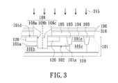
- another silicon dioxide layer 316 may be optionally formed on the hard mask layer 105 (see FIG. 3 ).
- the silicon dioxide layer 316 is served as a sacrificial layer for the etching back process 215 in order to adjust the etching depth and range of the etching back process 215 .
- a thermal oxidation process is performed to form a gate dielectric layer 109 on a sidewall 108 a of the trench 108 (see FIG. 2B ).
- a polysilicon layer 110 is formed on the remaining hard mask layer 105 and the exposed pad silicon oxide layer 104 , and filled into the trench 108 .
- a planarization process 111 e.g. a chemical mechanical polishing process
- a planarization process 111 is performed to remove the polysilicon layer 110 by using the hard mask layer 105 as a polish stop layer.
- a T-shaped polysilicon gate 214 is formed (see FIG. 2D ).
- the T-shaped polysilicon gate 214 is configured symmetrical with respect to a central line 108 b of the trench 108 .
- the T-shaped polysilicon gate 214 comprises an insertion portion 214 a and a symmetrical protrusion portion 214 b .
- the insertion portion 214 a is embedded in the trench 108 .
- the symmetrical protrusion portion 214 b is protruded over the surface 101 d of the substrate 101 , symmetrical with respect to the central line 108 b of the trench 108 , and externally and transversely extended from the central line 108 b of the trench 108 .
- a metal interconnection process is performed. Consequently, a dielectric material layer 117 is firstly formed over the surface 101 d of the substrate 101 and the polysilicon gate 214 , and then a plurality of metal contact plugs 118 are formed in the dielectric material layer 117 . Meanwhile, the trench gate metal oxide semiconductor field effect transistor 200 is produced. The resulting structure of the trench gate metal oxide semiconductor field effect transistor 200 is shown in FIG. 2E .
- the structure of the polysilicon gate 214 of the trench gate metal oxide semiconductor field effect transistor 200 is improved in comparison to the trench gate MOSFET 100 shown in FIGS. 1A ⁇ 1 F.
- a part of the hard mask layer 105 at the entrance 108 c of the trench 108 is firstly removed by an etching back process (e.g. an anisotropic etching process) (see FIG. 2A ) then the polysilicon layer 110 is filled into the trench 108 , and finally a planarization process is performed.
- an etching back process e.g. an anisotropic etching process
- the symmetrical protrusion portion 214 b of the polysilicon gate 214 can be symmetrically configured with respect to the central line 108 b of the trench 108 and transversely extended from the central line 108 b of the trench 108 (see FIG. 2D ).
- the symmetrical protrusion portion 114 b can provide a larger process window for subsequently forming of the metal contact plug 118 on the polysilicon gate 214 . Consequently, even if the feature size of the semiconductor device is shrunken down, the misalignment error thereof will be largely reduced.
- the fabricating method of the present invention only a single photolithography and etching process is sufficient to form a polysilicon gate, instead of requiring two photolithography and etching processes to form the same. Consequently, the fabricating method of the present invention is simplified, the photomask number is reduced, and the misalignment error of the semiconductor device is largely reduced. Since the misalignment error is largely reduced, the symmetrical protrusion portion of the polysilicon gate is no longer unexpectedly and asymmetrically extended in the transverse direction, and the total cumulative misalignment error of the semiconductor device is reduced.
- the present invention provides a trench gate metal oxide semiconductor field effect transistor and a fabricating method thereof.
- the fabricating method comprises the following steps. Firstly, a substrate is provided. Then, a hard mask layer is formed on the substrate. Then, an etching process is performed to remove a part of the hard mask layer and form a trench in the substrate. Then, an etching back process is performed to remove a part of the hard mask layer. Then, a polysilicon layer is formed on the hard mask layer and filled into the trench. Then, by using the hard mask layer as a stop layer, a planarization process is performed to remove the polysilicon layer. Consequently, a polysilicon gate with the symmetrical protrusion portion is formed.
- the symmetrical protrusion portion of the polysilicon gate can provide a larger process window for subsequently forming the metal contact plug on the polysilicon gate. Consequently, even if the feature size of the device is shrunken down, the misalignment error will be largely reduced.
- the symmetrical protrusion portion of the polysilicon gate is formed by etching back the hard mask layer to widen the entrance of the trench and then filling the polysilicon layer. Consequently, it is not necessary to perform an additional photolithography and etching process. In other words, the fabricating method of the present invention is simplified and cost-effective. Since it is not necessary to repeatedly use the photomask for alignment, the precision of the alignment between the metal contact plug and the polysilicon gate is enhanced.
Abstract
A trench gate metal oxide semiconductor field effect transistor includes a substrate and a gate. The substrate has a trench. The trench is extended downwardly from a surface of the substrate. The gate includes an insertion portion and a symmetrical protrusion portion. The insertion portion is embedded in the trench. The symmetrical protrusion portion is symmetrically protruded over the surface of the substrate.
Description
This application is a divisional application of a U.S. patent application Ser. No. 13/654,432, filed on Oct. 18, 2012, which application is incorporated by reference herein in its entirety.
The present invention relates to a semiconductor device and a fabricating method thereof, and more particularly to a trench gate metal oxide semiconductor field effect transistor and a fabricating method thereof.
A conventional trench gate metal oxide semiconductor field effect transistor comprises a gate structure, which is disposed within a trench. For fabricating the conventional trench gate metal oxide semiconductor field effect transistor, a trench is firstly formed in a semiconductor substrate, and then a gate dielectric layer is formed on a sidewall of the trench by thermal oxidation. Then, a polysilicon semiconductor material is filled into the trench. After a planarization process is performed, a polysilicon gate is formed in the trench.
Recently, since the integrated circuit becomes more complicated, the feature size and wiring space of the semiconductor device are gradually decreased, and the size of the polysilicon gate is reduced. After the polysilicon gate is formed, a metal contact plug is formed on the polysilicon gate in the subsequent process. As known, the size reduction of the polysilicon gate may result in misalignment between the polysilicon gate and the metal contact plug. If the metal contact plug is deviated because of misalignment, the metal contact plug and the neighboring circuits may be suffered from charge breakdown.
Therefore, there is a need of providing an improved trench gate metal oxide semiconductor field effect transistor and a fabricating method thereof in order to obviate the drawbacks encountered from the prior art.
In accordance with an aspect, the present invention provides a trench gate metal oxide semiconductor field effect transistor. The trench gate metal oxide semiconductor field effect transistor includes a substrate and a gate. The substrate has a trench. The trench is extended downwardly from a surface of the substrate. The gate includes an insertion portion and a symmetrical protrusion portion. The insertion portion is embedded in the trench. The symmetrical protrusion portion is symmetrically protruded over the surface of the substrate.
In an embodiment, the symmetrical protrusion portion is wider than the trench.
In an embodiment, the gate is a T-shaped gate, which is symmetrical with respect to a central line of the trench.
In an embodiment, the trench has a width smaller than or equal to 0.8 μm and a depth of about 1.6 μm.
In an embodiment, the trench gate metal oxide semiconductor field effect transistor includes a dielectric material layer and a contact plug. The dielectric material layer is disposed over the surface of the substrate and the gate. The contact plug is penetrated through the dielectric material layer and electrically contacted with the symmetrical protrusion portion of the gate.
In an embodiment, the trench gate metal oxide semiconductor field effect transistor includes a first-conductive doped region, a second-conductive doped region, a gate dielectric layer, and a source region. The first-conductive doped region is formed in the substrate. The second-conductive doped region is formed in the substrate. A P/N junction is formed between the first-conductive doped region and the second-conductive doped region. The trench is extended downwardly from the surface of the trench, penetrated through the first-conductive doped region and the P/N junction, and inserted into the second-conductive doped region. The gate dielectric layer is formed on a sidewall of the trench. The source region is formed in the substrate and located beside the gate dielectric layer.
In an embodiment, the first-conductive doped region is a P-type body region, and the second-conductive doped region is an N-type well region.
In an embodiment, the trench gate metal oxide semiconductor field effect transistor further includes an N-type buried layer, which is disposed under the second-conductive doped region.
In an embodiment, the source region is an N-type well region, and the source region is extended from the surface of the substrate into the first-conductive doped region.
In accordance with an aspect, the present invention provides a method for fabricating a trench gate metal oxide semiconductor field effect transistor. The method includes the following steps. Firstly, a substrate is provided. Then, a hard mask layer is formed on the substrate. Then, an etching process is performed to remove a part of the hard mask layer and form a trench in the substrate. Then, an etching back process is performed to remove a part of the hard mask layer. Then, a conductive layer is formed on the hard mask layer and filled into the trench. Then, a planarization process is performed to remove the conductive layer by using the hard mask layer as a stop layer.
In an embodiment, before the hard mask layer is formed, the method further includes a step of forming a pad silicon oxide layer on the substrate.
In an embodiment, after the hard mask layer is formed, the method further includes a step of forming a sacrificial layer on the hard mask layer.
In an embodiment, before the conductive layer is formed, the method further comprises a step of forming a gate dielectric layer on a sidewall of the trench by a thermal oxidation process.
In an embodiment, the hard mask layer is a silicon oxide layer or a silicon nitride layer.
The above objects and advantages of the present invention will become more readily apparent to those ordinarily skilled in the art after reviewing the following detailed description and accompanying drawings, in which:
The present invention will now be described more specifically with reference to the following embodiments. It is to be noted that the following descriptions of preferred embodiments of this invention are presented herein for purpose of illustration and description only. It is not intended to be exhaustive or to be limited to the precise form disclosed.
Firstly, as shown in FIG. 1A , a substrate 101 is provided. In an embodiment, the substrate 101 is a silicon substrate. In addition, the substrate 101 comprises a first-conductive doped region 101 a, a second-conductive doped region 101 b, a source region 120, and a second-conductive deep well region 101 c.
The first-conductive doped region 101 a, the second-conductive doped region 101 b, the source region 120 and the second-conductive deep well region 101 c are formed in the substrate 101 by a plurality of ion implantation processes. The second-conductive doped region 101 b is formed in the substrate 101. The first-conductive doped region 101 a is disposed over the second-conductive doped region 101 b, and extended downwardly from a surface 101 d of the substrate 101 to be contacted with the second-conductive doped region 101 b. Consequently, a P/N junction 102 is formed between the first-conductive doped region 101 a and the second-conductive doped region 101 b. The source region 120 is extended downwardly from the surface 101 d of the substrate 101, and formed in the first-conductive doped region 101 a. The second-conductive deep well region 101 c is formed in the substrate 101, and extended downwardly from the surface 101 d of the substrate 101, serving as the drain of the trench gate metal oxide semiconductor field effect transistor 100. Moreover, the second-conductive deep well region 101 c is contacted with the second-conductive doped region 101 b. Furthermore, a buried layer 119 with the same conductivity as the second-conductive doped region 101 b is disposed under the second-conductive doped region 101 b.
In this embodiment, the second-conductive doped region 101 b is an N-type well region with a lower dopant concentration. The first-conductive doped region 101 a is a P-type body region. The source region 120 is an N-type well region with a higher dopant concentration. The second-conductive deep well region 101 c is an N-type deep well region. The second-conductive deep well region 101 c is isolated from the first-conductive doped region 101 a through a shallow trench isolation structure 103. The buried layer 119 is an N-type doped region with a higher dopant concentration. The buried layer 119 is disposed under the second-conductive doped region 101 b and contacted with the second-conductive deep well region 101 c. Preferably, an N-type well region 101 e with a dopant concentration greater than that of the N-type (second-conductive) deep well region 101 c, maybe formed in the N-type (second-conductive) deep well region 101 c, and extended downwardly from the surface 101 d of the substrate 101.
Then, as shown in FIG. 1B , by film deposition processes or any other suitable processes, a pad silicon oxide layer 104, a hard mask layer 105 and a patterned photoresist layer 106 are formed on the surface 101 d of the substrate 101 to cover the second-conductive deep well region 101 c, the source region 120 and the first-conductive doped region 101 a. For example, the hard mask layer 105 is made of silicon nitride. Alternatively, the hard mask layer 105 may be made of silicon oxide.
Then, as shown in FIG. 1C , by using the patterned photoresist layer 106 as an etching mask, an etching process 107 is performed to remove a part of the hard mask layer 105, a part of the pad silicon oxide layer 104 and a part of the substrate 101. Consequently, a trench 108 is formed in the substrate 101. The trench 108 is extended downwardly from the surface 101 d of the substrate 101, penetrated through the source region 120, and extended into the second-conductive doped region 101 b. For example, the etching process 107 is a dry etching process. The trench 108 has a width smaller than or equal to 0.8 μm and a depth of about 1.6 μm.
After the patterned photoresist layer 106 and the remaining hard mask layer 105 are removed, a thermal oxidation process is performed to form a gate dielectric layer 109 on a sidewall 108 a of the trench 108 (see FIG. 1D ). Then, a conductive layer, preferably a polysilicon layer 110, is formed on the pad silicon oxide layer 104, and filled into the trench 108. Then, a planarization process 111 (e.g. a chemical mechanical polishing process) is performed to partially remove the polysilicon layer 110.
After the planarization process 111 is performed, a patterned photoresist layer 112 is formed on the polysilicon layer 110. By using the pad silicon oxide layer 104 as an etch stop layer, another etching process 113 is performed to remove a part of the planarized polysilicon layer 110. Consequently, a T-shaped portion of the planarized polysilicon layer 110 is remained and serves as a T-shaped polysilicon gate 114 of the trench gate metal oxide semiconductor field effect transistor 100 (see FIG. 1E ). The T-shaped polysilicon gate 114 comprises an insertion portion 114 a and a protrusion portion 114 b. The insertion portion 114 a is embedded in the trench 108. The protrusion portion 114 b is protruded over the surface 101 d of the substrate 101 and externally and transversely extended from a central line 108 b of the trench 108.
Then, a metal interconnection process is performed. Consequently, a dielectric material layer 117 is firstly formed over the surface 101 d of the substrate 101 and the polysilicon gate 114, and then a plurality of metal contact plugs 118 are formed in the dielectric material layer 117. Meanwhile, the trench gate metal oxide semiconductor field effect transistor 100 is produced. The resulting structure of the trench gate metal oxide semiconductor field effect transistor 100 is shown in FIG. 1F .
Please refer to FIG. 1F again. In the T-shaped polysilicon gate 114, the transversely-extending width of the protrusion portion 114 b is greater than the width of the insertion portion 114 a. Consequently, the protrusion portion 114 b can provide a larger process window for the subsequently forming of the metal contact plug 118 on the polysilicon gate 114.
However, the above-mentioned method for fabricating the trench gate metal oxide semiconductor field effect transistor 100 still has some drawbacks. For example, since two photolithography and etching processes are required to form the polysilicon gate 114, every misalignment error of the photomask may further decrease the alignment accuracy. Moreover, during the performing of the etching process 113, the surface 101 d of the substrate 101 is still completely covered by the planarized polysilicon layer 110. Since the alignment mark for the etching process 113 is possibly hindered by the planarized polysilicon layer 110, the misalignment error of the photomask is thereby increased. Due to the misalignment error of the photomask, the protrusion portion 114 b of the polysilicon gate 114 may be unexpectedly and asymmetrically extended in the transverse direction. If the (alignment) process errors in the process of forming the metal contact plug 118 are taken into consideration, the total cumulative misalignment error of the semiconductor device is very large. Under this circumstance, the metal contact plug 118 and the neighboring circuits may be suffered from charge breakdown.
For solving the above drawbacks, the method of forming the polysilicon gate 114 needs to be further improved.
Firstly, the steps as shown in FIGS. 1A, 1B and 1C are sequentially performed. After the trench 108 is formed (see FIG. 1C ), the remaining hard mask layer 105 is not removed immediately. On the other hand, as shown in FIG. 2A according to the embodiment of present invention, after the patterned photoresist layer 106 is removed, an etching back process 215 is performed to remove the patterned photoresist layer 106 and a part of the hard mask layer 105, and a part of the pad silicon oxide layer 104 at an entrance 108 c of the trench 108 that is exposed. In an embodiment, the hard mask layer 105 is made of silicon nitride, and the etching back process 215 is a wet etching process by using a phosphoric acid solution as an etchant solution to remove a part of the hard mask layer 105. Alternatively, in another embodiment, the hard mask layer 105 is made of silicon dioxide, and the etching back process 215 is a wet etching process by using a buffer oxide etcher (BOE) solution as an etchant solution to remove a part of the hard mask layer 105.
Furthermore, for improved control of the etching back process 215, before the patterned photoresist layer 106 is formed, another silicon dioxide layer 316 may be optionally formed on the hard mask layer 105 (see FIG. 3 ). The silicon dioxide layer 316 is served as a sacrificial layer for the etching back process 215 in order to adjust the etching depth and range of the etching back process 215.
Then, a thermal oxidation process is performed to form a gate dielectric layer 109 on a sidewall 108 a of the trench 108 (see FIG. 2B ). Then, as shown in FIG. 2C , a polysilicon layer 110 is formed on the remaining hard mask layer 105 and the exposed pad silicon oxide layer 104, and filled into the trench 108.
Then, a planarization process 111 (e.g. a chemical mechanical polishing process) is performed to remove the polysilicon layer 110 by using the hard mask layer 105 as a polish stop layer. After the remaining hard mask layer 105 is removed, a T-shaped polysilicon gate 214 is formed (see FIG. 2D ). The T-shaped polysilicon gate 214 is configured symmetrical with respect to a central line 108 b of the trench 108. The T-shaped polysilicon gate 214 comprises an insertion portion 214 a and a symmetrical protrusion portion 214 b. The insertion portion 214 a is embedded in the trench 108. The symmetrical protrusion portion 214 b is protruded over the surface 101 d of the substrate 101, symmetrical with respect to the central line 108 b of the trench 108, and externally and transversely extended from the central line 108 b of the trench 108.
Then, a metal interconnection process is performed. Consequently, a dielectric material layer 117 is firstly formed over the surface 101 d of the substrate 101 and the polysilicon gate 214, and then a plurality of metal contact plugs 118 are formed in the dielectric material layer 117. Meanwhile, the trench gate metal oxide semiconductor field effect transistor 200 is produced. The resulting structure of the trench gate metal oxide semiconductor field effect transistor 200 is shown in FIG. 2E .
From the above discussions, the structure of the polysilicon gate 214 of the trench gate metal oxide semiconductor field effect transistor 200 is improved in comparison to the trench gate MOSFET 100 shown in FIGS. 1A ˜1F. For forming the polysilicon gate 214, a part of the hard mask layer 105 at the entrance 108 c of the trench 108 is firstly removed by an etching back process (e.g. an anisotropic etching process) (see FIG. 2A ) then the polysilicon layer 110 is filled into the trench 108, and finally a planarization process is performed. Consequently, the symmetrical protrusion portion 214 b of the polysilicon gate 214 can be symmetrically configured with respect to the central line 108 b of the trench 108 and transversely extended from the central line 108 b of the trench 108 (see FIG. 2D ). The symmetrical protrusion portion 114 b can provide a larger process window for subsequently forming of the metal contact plug 118 on the polysilicon gate 214. Consequently, even if the feature size of the semiconductor device is shrunken down, the misalignment error thereof will be largely reduced.
Moreover, according to the embodiments of the fabricating method of the present invention, only a single photolithography and etching process is sufficient to form a polysilicon gate, instead of requiring two photolithography and etching processes to form the same. Consequently, the fabricating method of the present invention is simplified, the photomask number is reduced, and the misalignment error of the semiconductor device is largely reduced. Since the misalignment error is largely reduced, the symmetrical protrusion portion of the polysilicon gate is no longer unexpectedly and asymmetrically extended in the transverse direction, and the total cumulative misalignment error of the semiconductor device is reduced.
From the above discussions, the present invention provides a trench gate metal oxide semiconductor field effect transistor and a fabricating method thereof. The fabricating method comprises the following steps. Firstly, a substrate is provided. Then, a hard mask layer is formed on the substrate. Then, an etching process is performed to remove a part of the hard mask layer and form a trench in the substrate. Then, an etching back process is performed to remove a part of the hard mask layer. Then, a polysilicon layer is formed on the hard mask layer and filled into the trench. Then, by using the hard mask layer as a stop layer, a planarization process is performed to remove the polysilicon layer. Consequently, a polysilicon gate with the symmetrical protrusion portion is formed.
The symmetrical protrusion portion of the polysilicon gate can provide a larger process window for subsequently forming the metal contact plug on the polysilicon gate. Consequently, even if the feature size of the device is shrunken down, the misalignment error will be largely reduced.
From the above descriptions, the symmetrical protrusion portion of the polysilicon gate is formed by etching back the hard mask layer to widen the entrance of the trench and then filling the polysilicon layer. Consequently, it is not necessary to perform an additional photolithography and etching process. In other words, the fabricating method of the present invention is simplified and cost-effective. Since it is not necessary to repeatedly use the photomask for alignment, the precision of the alignment between the metal contact plug and the polysilicon gate is enhanced.
While the invention has been described in terms of what is presently considered to be the most practical and preferred embodiments, it is to be understood that the invention needs not be limited to the disclosed embodiment. On the contrary, it is intended to cover various modifications and similar arrangements included within the spirit and scope of the appended claims which are to be accorded with the broadest interpretation so as to encompass all such modifications and similar structures.
Claims (11)
1. A method for fabricating a trench gate metal oxide semiconductor field effect transistor, the method comprising steps of:
providing a substrate having a source region;
forming an oxide layer on the substrate;
forming a hard mask layer on the oxide layer;
performing an etching process to remove a part of the hard mask layer, a part of the oxide layer, a part of the substrate to form a trench in the substrate penetrating the source region;
performing an etching back process to remove a part of the remaining hard mask layer to expose a part of the oxide layer;
performing a thermal oxidation process to form a gate dielectric layer only on a sidewall of the trench;
forming a conductive layer covering on the hard mask layer and the exposed part of the oxide layer, and filling the conductive layer into the trench;
performing a chemical mechanical polishing process to remove a portion of the conductive layer on the hard mask layer by using the hard mask layer as a stop layer and leave behind a T-shaped portion of the conductive layer with an insertion portion embedded in the trench and a symmetrical protrusion portion on the substrate; and
forming a contact plug on the surface of the substrate contacting the T-shaped portion of the conductive layer.
2. The method according to claim 1 , wherein the oxide layer is a pad silicon oxide layer.
3. The method according to claim 1 , wherein after the hard mask layer is formed, the method further comprises a step of forming a sacrificial layer on the hard mask layer.
4. The method according to claim 1 , wherein the hard mask layer is a silicon oxide layer or a silicon nitride layer.
5. The method according to claim 2 , wherein the symmetrical protrusion portion of the conductive layer covering a portion of the pad silicon oxide layer on the substrate.
6. The method according to claim 1 , wherein the step of performing a thermal oxidation process to form the gate dielectric layer is performed directly after the step of performing the etching back process.
7. The method according to claim 1 , wherein the symmetrical protrusion portion on the substrate covering a portion of the source region.
8. The method according to claim 1 , wherein the the symmetrical protrusion portion is symmetrical with respect to the insertion portion on the substrate.
9. The method according to claim 1 , wherein the etching back process is a wet etching process.
10. The method according to claim 1 , wherein the contact plug is attached to the symmetrical protrusion portion of the T-shaped portion of the conductive layer.
11. The method according to claim 1 , after the step of performing the chemical mechanical polishing process and before the step of forming the contact plug, further comprising:
forming a dielectric material layer over the surface of the substrate and the T-shaped portion of the conductive layer; and
removing a portion of the dielectric material layer and a portion of the oxide layer.
Priority Applications (1)
| Application Number | Priority Date | Filing Date | Title |
|---|---|---|---|
| US14/754,636 US9525037B2 (en) | 2012-10-18 | 2015-06-29 | Fabricating method of trench gate metal oxide semiconductor field effect transistor |
Applications Claiming Priority (2)
| Application Number | Priority Date | Filing Date | Title |
|---|---|---|---|
| US13/654,432 US20140110777A1 (en) | 2012-10-18 | 2012-10-18 | Trench gate metal oxide semiconductor field effect transistor and fabricating method thereof |
| US14/754,636 US9525037B2 (en) | 2012-10-18 | 2015-06-29 | Fabricating method of trench gate metal oxide semiconductor field effect transistor |
Related Parent Applications (1)
| Application Number | Title | Priority Date | Filing Date |
|---|---|---|---|
| US13/654,432 Division US20140110777A1 (en) | 2012-10-18 | 2012-10-18 | Trench gate metal oxide semiconductor field effect transistor and fabricating method thereof |
Publications (2)
| Publication Number | Publication Date |
|---|---|
| US20150318366A1 US20150318366A1 (en) | 2015-11-05 |
| US9525037B2 true US9525037B2 (en) | 2016-12-20 |
Family
ID=50484580
Family Applications (2)
| Application Number | Title | Priority Date | Filing Date |
|---|---|---|---|
| US13/654,432 Abandoned US20140110777A1 (en) | 2012-10-18 | 2012-10-18 | Trench gate metal oxide semiconductor field effect transistor and fabricating method thereof |
| US14/754,636 Active US9525037B2 (en) | 2012-10-18 | 2015-06-29 | Fabricating method of trench gate metal oxide semiconductor field effect transistor |
Family Applications Before (1)
| Application Number | Title | Priority Date | Filing Date |
|---|---|---|---|
| US13/654,432 Abandoned US20140110777A1 (en) | 2012-10-18 | 2012-10-18 | Trench gate metal oxide semiconductor field effect transistor and fabricating method thereof |
Country Status (1)
| Country | Link |
|---|---|
| US (2) | US20140110777A1 (en) |
Families Citing this family (5)
| Publication number | Priority date | Publication date | Assignee | Title |
|---|---|---|---|---|
| TWI559531B (en) * | 2014-08-20 | 2016-11-21 | 新唐科技股份有限公司 | Insulated gate bipolar transistor and method of manufacturing the same |
| WO2016204794A1 (en) | 2015-06-19 | 2016-12-22 | Intel Corporation | Vertical transistor using a through silicon via gate |
| US9264944B1 (en) | 2015-07-06 | 2016-02-16 | Peerless Network, Inc. | SBC-localized handoff |
| DE102016108943B4 (en) * | 2016-05-13 | 2019-03-07 | Infineon Technologies Austria Ag | Method for forming semiconductor devices, semiconductor devices and power semiconductor devices |
| KR20220037282A (en) * | 2020-09-17 | 2022-03-24 | 삼성전자주식회사 | Semiconductor device and electronic system |
Citations (117)
| Publication number | Priority date | Publication date | Assignee | Title |
|---|---|---|---|---|
| US4344081A (en) | 1980-04-14 | 1982-08-10 | Supertex, Inc. | Combined DMOS and a vertical bipolar transistor device and fabrication method therefor |
| US4396999A (en) | 1981-06-30 | 1983-08-02 | International Business Machines Corporation | Tunneling transistor memory cell |
| US4893160A (en) | 1987-11-13 | 1990-01-09 | Siliconix Incorporated | Method for increasing the performance of trenched devices and the resulting structure |
| US4918333A (en) | 1988-10-31 | 1990-04-17 | Anderson Floyd E | Microprocessor having high current drive |
| US4958089A (en) | 1988-12-20 | 1990-09-18 | Gazelle Microcircuits, Inc. | High output drive FET buffer for providing high initial current to a subsequent stage |
| US5016068A (en) | 1988-04-15 | 1991-05-14 | Texas Instruments Incorporated | Vertical floating-gate transistor |
| US5016065A (en) | 1988-11-04 | 1991-05-14 | Sharp Kabushiki Kaisha | Compound semiconductor substrate with InGaP layer |
| US5040045A (en) | 1990-05-17 | 1991-08-13 | U.S. Philips Corporation | High voltage MOS transistor having shielded crossover path for a high voltage connection bus |
| US5071782A (en) | 1990-06-28 | 1991-12-10 | Texas Instruments Incorporated | Vertical memory cell array and method of fabrication |
| US5124761A (en) | 1988-01-22 | 1992-06-23 | Sony Corporation | Semiconductor apparatus |
| US5124764A (en) | 1986-10-21 | 1992-06-23 | Texas Instruments Incorporated | Symmetric vertical MOS transistor with improved high voltage operation |
| US5126807A (en) | 1990-06-13 | 1992-06-30 | Kabushiki Kaisha Toshiba | Vertical MOS transistor and its production method |
| US5268589A (en) | 1990-09-28 | 1993-12-07 | Siemens Aktiengesellschaft | Semiconductor chip having at least one electrical resistor means |
| US5296393A (en) | 1990-11-23 | 1994-03-22 | Texas Instruments Incorporated | Process for the simultaneous fabrication of high-and-low-voltage semiconductor devices, integrated circuit containing the same, systems and methods |
| US5326711A (en) | 1993-01-04 | 1994-07-05 | Texas Instruments Incorporated | High performance high voltage vertical transistor and method of fabrication |
| US5346835A (en) | 1992-07-06 | 1994-09-13 | Texas Instruments Incorporated | Triple diffused lateral resurf insulated gate field effect transistor compatible with process and method |
| US5430316A (en) | 1992-02-18 | 1995-07-04 | Sgs-Thomson Microeletronics, S.R.L. | VDMOS transistor with improved breakdown characteristics |
| US5436486A (en) | 1992-10-19 | 1995-07-25 | Fuji Electric Co., Ltd. | High voltage MIS transistor and semiconductor device |
| US5534721A (en) | 1994-11-30 | 1996-07-09 | At&T Corp. | Area-efficient layout for high voltage lateral devices |
| US5614751A (en) | 1995-01-10 | 1997-03-25 | Siliconix Incorporated | Edge termination structure for power MOSFET |
| US5698893A (en) | 1995-01-03 | 1997-12-16 | Motorola, Inc. | Static-random-access memory cell with trench transistor and enhanced stability |
| US5811850A (en) | 1994-10-14 | 1998-09-22 | Texas Instruments Incorporated | LDMOS transistors, systems and methods |
| US5950090A (en) | 1998-11-16 | 1999-09-07 | United Microelectronics Corp. | Method for fabricating a metal-oxide semiconductor transistor |
| US5998301A (en) | 1997-12-18 | 1999-12-07 | Advanced Micro Devices, Inc. | Method and system for providing tapered shallow trench isolation structure profile |
| US6066884A (en) | 1999-03-19 | 2000-05-23 | Lucent Technologies Inc. | Schottky diode guard ring structures |
| US6077733A (en) * | 1999-09-03 | 2000-06-20 | Taiwan Semiconductor Manufacturing Company | Method of manufacturing self-aligned T-shaped gate through dual damascene |
| US6124611A (en) | 1998-10-30 | 2000-09-26 | Sony Corporation | Epitaxial channel vertical MOS transistor |
| US6144538A (en) | 1999-12-20 | 2000-11-07 | United Microelectronics Corp. | High voltage MOS transistor used in protection circuits |
| US6165846A (en) | 1999-03-02 | 2000-12-26 | Zilog, Inc. | Method of eliminating gate leakage in nitrogen annealed oxides |
| US6184142B1 (en) * | 1999-04-26 | 2001-02-06 | United Microelectronics Corp. | Process for low k organic dielectric film etch |
| US6204123B1 (en) | 1998-10-30 | 2001-03-20 | Sony Corporation | Vertical floating gate transistor with epitaxial channel |
| US6245689B1 (en) | 1996-09-05 | 2001-06-12 | Advanced Micro Devices, Inc. | Process for reliable ultrathin oxynitride formation |
| US6271128B1 (en) * | 2000-09-29 | 2001-08-07 | Vanguard International Semiconductor Corp. | Method for fabricating transistor |
| US6277675B1 (en) | 1999-10-28 | 2001-08-21 | United Microelectronics Corp. | Method of fabricating high voltage MOS device |
| US6277757B1 (en) | 1999-06-01 | 2001-08-21 | Winbond Electronics Corp. | Methods to modify wet by dry etched via profile |
| US6297108B1 (en) | 2000-03-10 | 2001-10-02 | United Microelectronics Corp. | Method of forming a high voltage MOS transistor on a semiconductor wafer |
| US6306700B1 (en) | 2000-08-07 | 2001-10-23 | United Microelectronics Corp. | Method for forming high voltage devices compatible with low voltages devices on semiconductor substrate |
| US6326283B1 (en) | 2000-03-07 | 2001-12-04 | Vlsi Technology, Inc. | Trench-diffusion corner rounding in a shallow-trench (STI) process |
| US6353247B1 (en) | 2000-04-15 | 2002-03-05 | United Microelectronics Corp. | High voltage electrostatic discharge protection circuit |
| US6388292B1 (en) | 1997-09-16 | 2002-05-14 | Winbond Electronics Corporation | Distributed MOSFET structure with enclosed gate for improved transistor size/layout area ratio and uniform ESD triggering |
| US6400003B1 (en) | 1998-02-12 | 2002-06-04 | Koninklijke Philips Electronics N.V. | High voltage MOSFET with geometrical depletion layer enhancement |
| US6403456B1 (en) * | 2000-08-22 | 2002-06-11 | Advanced Micro Devices, Inc. | T or T/Y gate formation using trim etch processing |
| US6424005B1 (en) | 1998-12-03 | 2002-07-23 | Texas Instruments Incorporated | LDMOS power device with oversized dwell |
| US20020158277A1 (en) | 2001-03-28 | 2002-10-31 | Hirofumi Harada | Semiconductor integrated circuit device and manufacturing method therefor |
| US20030022460A1 (en) | 2001-07-30 | 2003-01-30 | Samsung Electronics Co., Ltd. | Semiconductor device fabricating method |
| US6514830B1 (en) | 2000-03-22 | 2003-02-04 | Advanced Micro Devices, Inc. | Method of manufacturing high voltage transistor with modified field implant mask |
| US6521538B2 (en) | 2000-02-28 | 2003-02-18 | Denso Corporation | Method of forming a trench with a rounded bottom in a semiconductor device |
| US6614089B2 (en) | 1999-06-30 | 2003-09-02 | Kabushiki Kaisha Toshiba | Field effect transistor |
| US20040018698A1 (en) | 1997-04-23 | 2004-01-29 | Altera Corporation | Adjustable threshold isolation transistor |
| US6713794B2 (en) | 2000-07-04 | 2004-03-30 | Kabushiki Kaisha Toshiba | Lateral semiconductor device |
| US20040070050A1 (en) | 2002-10-10 | 2004-04-15 | Taiwan Semiconductor Manufacturing Company | Structures of vertical resistors and FETs as controlled by electrical field penetration and a band-gap voltage reference using vertical FETs operating in accumulation through the field penetration effect |
| US6762098B2 (en) | 2000-10-06 | 2004-07-13 | General Semiconductor, Inc. | Trench DMOS transistor with embedded trench schottky rectifier |
| US6764890B1 (en) | 2003-01-29 | 2004-07-20 | Cypress Semiconductor Corporation | Method of adjusting the threshold voltage of a mosfet |
| US6784490B1 (en) | 1999-09-24 | 2004-08-31 | Matsushita Electric Industrial Co., Ltd. | High-voltage MOS transistor |
| US6784060B2 (en) | 2002-10-29 | 2004-08-31 | Hynix Semiconductor Inc. | Method for fabricating high voltage and low voltage transistors |
| US6819184B2 (en) | 2002-11-06 | 2004-11-16 | Cree Microwave, Inc. | RF transistor amplifier linearity using suppressed third order transconductance |
| US6822296B2 (en) | 2002-10-02 | 2004-11-23 | Topro Technology, Inc. | Complementary metal oxide semiconductor structure for battery protection circuit and battery protection circuit having the same |
| US6825531B1 (en) | 2003-07-11 | 2004-11-30 | Micrel, Incorporated | Lateral DMOS transistor with a self-aligned drain region |
| US6833584B2 (en) | 2001-06-08 | 2004-12-21 | Infineon Technologies Ag | Trench power semiconductor |
| US6846729B2 (en) | 2001-10-01 | 2005-01-25 | International Rectifier Corporation | Process for counter doping N-type silicon in Schottky device Ti silicide barrier |
| US6855581B2 (en) | 2001-12-26 | 2005-02-15 | Electronics And Telecommunications Research Institute | Method for fabricating a high-voltage high-power integrated circuit device |
| US6855980B2 (en) | 2000-09-20 | 2005-02-15 | Silicon Storage Technology, Inc. | Semiconductor memory array of floating gate memory cells with low resistance source regions and high source coupling |
| US6869848B2 (en) | 2003-06-05 | 2005-03-22 | Hynix Semiconductor Inc. | Method of manufacturing flash memory device |
| US6894349B2 (en) | 2001-06-08 | 2005-05-17 | Intersil Americas Inc. | Lateral DMOS structure with lateral extension structure for reduced charge trapping in gate oxide |
| US20050227448A1 (en) | 2004-04-07 | 2005-10-13 | Fu-Hsin Chen | High voltage double diffused drain MOS transistor with medium operation voltage |
| US6958515B2 (en) | 2000-12-31 | 2005-10-25 | Texas Instruments Incorporated | N-channel LDMOS with buried p-type region to prevent parasitic bipolar effects |
| US20050258496A1 (en) | 2002-12-17 | 2005-11-24 | Hideaki Tsuchiko | Integrated circuit including a high voltage bipolar device and low voltage devices |
| US20060035437A1 (en) | 2004-08-12 | 2006-02-16 | Noriyuki Mitsuhira | Semiconductor device having dual-STI and manufacturing method thereof |
| US7008832B1 (en) * | 2000-07-20 | 2006-03-07 | Advanced Micro Devices, Inc. | Damascene process for a T-shaped gate electrode |
| US7015116B1 (en) | 2002-09-20 | 2006-03-21 | Integrated Device Technology, Inc. | Stress-relieved shallow trench isolation (STI) structure and method for forming the same |
| US7023050B2 (en) | 2003-07-11 | 2006-04-04 | Salama C Andre T | Super junction / resurf LDMOST (SJR-LDMOST) |
| US7037788B2 (en) | 2000-05-30 | 2006-05-02 | Denso Corporation | Manufacturing method of semiconductor device |
| US7075575B2 (en) | 2000-11-06 | 2006-07-11 | Isetex, Inc. | Gated vertical punch through device used as a high performance charge detection amplifier |
| US7091079B2 (en) | 2004-11-11 | 2006-08-15 | United Microelectronics Corp. | Method of forming devices having three different operation voltages |
| US20060261407A1 (en) | 2004-11-09 | 2006-11-23 | Fultec Semiconductors Inc. | High-voltage transistor fabrication with trench etching technique |
| US20060270171A1 (en) | 2005-05-25 | 2006-11-30 | Li-Che Chen | MOS transistor device structure combining Si-trench and field plate structures for high voltage device |
| US20060270134A1 (en) | 2005-05-26 | 2006-11-30 | Wen-Fang Lee | High-voltage metal-oxide-semiconductor devices and method of making the same |
| US7148540B2 (en) | 2004-06-28 | 2006-12-12 | Agere Systems Inc. | Graded conductive structure for use in a metal-oxide-semiconductor device |
| US20070041227A1 (en) | 2005-08-18 | 2007-02-22 | Hall Jefferson W | Method of forming a start-up device and structure therefor |
| US20070082440A1 (en) | 2005-10-11 | 2007-04-12 | Elpida Memory, Inc. | Semiconductor device and manufacturing method thereof |
| US7214591B2 (en) | 2004-06-07 | 2007-05-08 | United Microelectronics Corp. | Method of fabricating high-voltage MOS device |
| US20070132033A1 (en) | 2005-12-12 | 2007-06-14 | Taiwan Semiconductor Manufacturing Company, Ltd. | High voltage CMOS devices |
| US20070138566A1 (en) | 2005-12-16 | 2007-06-21 | Hirokatsu Suzuki | Semiconductor device and manufacturing method of the same |
| US20070273001A1 (en) | 2006-05-24 | 2007-11-29 | Jung-Ching Chen | System on chip and method for manufacturing the same |
| US7309636B2 (en) | 2005-11-07 | 2007-12-18 | United Microelectronics Corp. | High-voltage metal-oxide-semiconductor device and method of manufacturing the same |
| US7323740B2 (en) | 2003-06-20 | 2008-01-29 | Samsung Electronics Co., Ltd | Single chip data processing device with embedded nonvolatile memory and method thereof |
| US20080160697A1 (en) | 2005-08-09 | 2008-07-03 | Ching-Hung Kao | Metal-oxide-semiconductor transistor and method of manufacturing the same |
| US20080160706A1 (en) | 2006-12-27 | 2008-07-03 | Jin Hyo Jung | Method for fabricating semiconductor device |
| US20080185629A1 (en) | 2007-02-01 | 2008-08-07 | Denso Corporation | Semiconductor device having variable operating information |
| US20080185642A1 (en) | 2004-10-29 | 2008-08-07 | International Rectifier Corporation | Trench MOSFET with deposited oxide |
| US7427552B2 (en) | 2005-12-05 | 2008-09-23 | Semiconductor Manufacturing International (Shanghai) Corporation | Method for fabricating isolation structures for flash memory semiconductor devices |
| US20080296655A1 (en) | 2007-05-31 | 2008-12-04 | United Microelectronics Corp. | Multi-time programmable memory and method of manufacturing the same |
| US20080315346A1 (en) | 2004-01-31 | 2008-12-25 | Ralf Lerner | Passivation of Deep Isolating Separating Trenches with Sunk Covering Layers |
| US20090065861A1 (en) * | 2005-02-11 | 2009-03-12 | Alpha & Omega Semiconductor Limited | MOS device with low injection diode |
| US20090108348A1 (en) | 2007-10-25 | 2009-04-30 | United Microelectronics Corp. | Semiconductor device |
| US20090111252A1 (en) | 2007-10-30 | 2009-04-30 | United Microelectronics Corp. | Method for forming deep well region of high voltage device |
| US20090159966A1 (en) | 2007-12-20 | 2009-06-25 | Chih-Jen Huang | High voltage semiconductor device, method of fabricating the same, and method of fabricating the same and a low voltage semiconductor device together on a substrate |
| US20090176342A1 (en) * | 2008-01-03 | 2009-07-09 | Samsung Electronics Co., Ltd. | Method of fabricating semiconductor device having deifferential gate dielectric layer and related device |
| US20090197380A1 (en) * | 2007-12-27 | 2009-08-06 | Kyu-Ok Lee | Method for manufacturing a recessed gate transistor |
| TW200939472A (en) | 2007-12-21 | 2009-09-16 | Alpha & Omega Semiconductor | MOS device with varying trench depth |
| US20090233409A1 (en) * | 2008-03-17 | 2009-09-17 | Sony Corporation | Method for production of semiconductor device |
| US20090278208A1 (en) | 2006-01-12 | 2009-11-12 | Dong-Ryul Chang | Semiconductor integrated circuit device and method of fabricating the same |
| US7622764B2 (en) | 2003-12-31 | 2009-11-24 | Dongbu Electronics Co., Ltd. | Semiconductor device and fabricating method thereof |
| US20090294870A1 (en) | 2008-05-27 | 2009-12-03 | Nec Electronics Corporation | Semiconductor device with trench gate and method of manufacturing the same |
| US20090294865A1 (en) | 2008-05-27 | 2009-12-03 | Chien-Shao Tang | Schottky Diodes Having Low-Voltage and High-Concentration Rings |
| US20100006937A1 (en) | 2008-07-09 | 2010-01-14 | Yong Jun Lee | Lateral Double Diffused Metal Oxide Semiconductor (LDMOS) Device and Method of Manufacturing LDMOS Device |
| US20100032758A1 (en) | 2008-08-06 | 2010-02-11 | United Microelectronics Corp. | Ldmos device for esd protection circuit |
| US20100096702A1 (en) | 2008-10-17 | 2010-04-22 | United Microelectronics Corp. | Semiconductor device and method of fabricating the same |
| US20100148250A1 (en) | 2008-12-11 | 2010-06-17 | United Microelectronics Corp. | Metal oxide semiconductor device |
| US20100213517A1 (en) | 2007-10-19 | 2010-08-26 | Nxp B.V. | High voltage semiconductor device |
| US20110057263A1 (en) | 2009-09-10 | 2011-03-10 | Sung-Nien Tang | Ultra high voltage mos transistor device |
| US20110254082A1 (en) * | 2010-04-15 | 2011-10-20 | Hynix Semiconductor Inc. | Semiconductor device and method for forming the same |
| US20120061748A1 (en) | 2010-09-14 | 2012-03-15 | Naoto Kobayashi | Semiconductor device and method of manufacturing the same |
| US20120129306A1 (en) * | 2006-01-24 | 2012-05-24 | Yongzhong Hu | Configuration and method to form mosfet devices with low resistance silicide gate and mesa contact regions |
| US8232610B2 (en) | 2005-05-20 | 2012-07-31 | Renesas Electronics Corporation | Semiconductor device and manufacturing method of the same |
| US20120217513A1 (en) | 2011-02-28 | 2012-08-30 | Hitachi, Ltd. | Silicon carbide semiconductor device and manufacturing method thereof |
| US8652763B2 (en) * | 2007-07-16 | 2014-02-18 | The Board Of Trustees Of The University Of Illinois | Method for fabricating dual damascene profiles using sub pixel-voting lithography and devices made by same |
-
2012
- 2012-10-18 US US13/654,432 patent/US20140110777A1/en not_active Abandoned
-
2015
- 2015-06-29 US US14/754,636 patent/US9525037B2/en active Active
Patent Citations (119)
| Publication number | Priority date | Publication date | Assignee | Title |
|---|---|---|---|---|
| US4344081A (en) | 1980-04-14 | 1982-08-10 | Supertex, Inc. | Combined DMOS and a vertical bipolar transistor device and fabrication method therefor |
| US4396999A (en) | 1981-06-30 | 1983-08-02 | International Business Machines Corporation | Tunneling transistor memory cell |
| US5124764A (en) | 1986-10-21 | 1992-06-23 | Texas Instruments Incorporated | Symmetric vertical MOS transistor with improved high voltage operation |
| US4893160A (en) | 1987-11-13 | 1990-01-09 | Siliconix Incorporated | Method for increasing the performance of trenched devices and the resulting structure |
| US5124761A (en) | 1988-01-22 | 1992-06-23 | Sony Corporation | Semiconductor apparatus |
| US5016068A (en) | 1988-04-15 | 1991-05-14 | Texas Instruments Incorporated | Vertical floating-gate transistor |
| US4918333A (en) | 1988-10-31 | 1990-04-17 | Anderson Floyd E | Microprocessor having high current drive |
| US5016065A (en) | 1988-11-04 | 1991-05-14 | Sharp Kabushiki Kaisha | Compound semiconductor substrate with InGaP layer |
| US4958089A (en) | 1988-12-20 | 1990-09-18 | Gazelle Microcircuits, Inc. | High output drive FET buffer for providing high initial current to a subsequent stage |
| US5040045A (en) | 1990-05-17 | 1991-08-13 | U.S. Philips Corporation | High voltage MOS transistor having shielded crossover path for a high voltage connection bus |
| US5126807A (en) | 1990-06-13 | 1992-06-30 | Kabushiki Kaisha Toshiba | Vertical MOS transistor and its production method |
| US5071782A (en) | 1990-06-28 | 1991-12-10 | Texas Instruments Incorporated | Vertical memory cell array and method of fabrication |
| US5268589A (en) | 1990-09-28 | 1993-12-07 | Siemens Aktiengesellschaft | Semiconductor chip having at least one electrical resistor means |
| US5296393A (en) | 1990-11-23 | 1994-03-22 | Texas Instruments Incorporated | Process for the simultaneous fabrication of high-and-low-voltage semiconductor devices, integrated circuit containing the same, systems and methods |
| US5430316A (en) | 1992-02-18 | 1995-07-04 | Sgs-Thomson Microeletronics, S.R.L. | VDMOS transistor with improved breakdown characteristics |
| US5346835A (en) | 1992-07-06 | 1994-09-13 | Texas Instruments Incorporated | Triple diffused lateral resurf insulated gate field effect transistor compatible with process and method |
| US5436486A (en) | 1992-10-19 | 1995-07-25 | Fuji Electric Co., Ltd. | High voltage MIS transistor and semiconductor device |
| US5326711A (en) | 1993-01-04 | 1994-07-05 | Texas Instruments Incorporated | High performance high voltage vertical transistor and method of fabrication |
| US5811850A (en) | 1994-10-14 | 1998-09-22 | Texas Instruments Incorporated | LDMOS transistors, systems and methods |
| US5534721A (en) | 1994-11-30 | 1996-07-09 | At&T Corp. | Area-efficient layout for high voltage lateral devices |
| US5698893A (en) | 1995-01-03 | 1997-12-16 | Motorola, Inc. | Static-random-access memory cell with trench transistor and enhanced stability |
| US5614751A (en) | 1995-01-10 | 1997-03-25 | Siliconix Incorporated | Edge termination structure for power MOSFET |
| US6245689B1 (en) | 1996-09-05 | 2001-06-12 | Advanced Micro Devices, Inc. | Process for reliable ultrathin oxynitride formation |
| US20040018698A1 (en) | 1997-04-23 | 2004-01-29 | Altera Corporation | Adjustable threshold isolation transistor |
| US6388292B1 (en) | 1997-09-16 | 2002-05-14 | Winbond Electronics Corporation | Distributed MOSFET structure with enclosed gate for improved transistor size/layout area ratio and uniform ESD triggering |
| US5998301A (en) | 1997-12-18 | 1999-12-07 | Advanced Micro Devices, Inc. | Method and system for providing tapered shallow trench isolation structure profile |
| US6400003B1 (en) | 1998-02-12 | 2002-06-04 | Koninklijke Philips Electronics N.V. | High voltage MOSFET with geometrical depletion layer enhancement |
| US6124611A (en) | 1998-10-30 | 2000-09-26 | Sony Corporation | Epitaxial channel vertical MOS transistor |
| US6204123B1 (en) | 1998-10-30 | 2001-03-20 | Sony Corporation | Vertical floating gate transistor with epitaxial channel |
| US5950090A (en) | 1998-11-16 | 1999-09-07 | United Microelectronics Corp. | Method for fabricating a metal-oxide semiconductor transistor |
| US6424005B1 (en) | 1998-12-03 | 2002-07-23 | Texas Instruments Incorporated | LDMOS power device with oversized dwell |
| US6165846A (en) | 1999-03-02 | 2000-12-26 | Zilog, Inc. | Method of eliminating gate leakage in nitrogen annealed oxides |
| US6066884A (en) | 1999-03-19 | 2000-05-23 | Lucent Technologies Inc. | Schottky diode guard ring structures |
| US6184142B1 (en) * | 1999-04-26 | 2001-02-06 | United Microelectronics Corp. | Process for low k organic dielectric film etch |
| US6277757B1 (en) | 1999-06-01 | 2001-08-21 | Winbond Electronics Corp. | Methods to modify wet by dry etched via profile |
| US6614089B2 (en) | 1999-06-30 | 2003-09-02 | Kabushiki Kaisha Toshiba | Field effect transistor |
| US6077733A (en) * | 1999-09-03 | 2000-06-20 | Taiwan Semiconductor Manufacturing Company | Method of manufacturing self-aligned T-shaped gate through dual damascene |
| US6784490B1 (en) | 1999-09-24 | 2004-08-31 | Matsushita Electric Industrial Co., Ltd. | High-voltage MOS transistor |
| US6277675B1 (en) | 1999-10-28 | 2001-08-21 | United Microelectronics Corp. | Method of fabricating high voltage MOS device |
| US6144538A (en) | 1999-12-20 | 2000-11-07 | United Microelectronics Corp. | High voltage MOS transistor used in protection circuits |
| US6521538B2 (en) | 2000-02-28 | 2003-02-18 | Denso Corporation | Method of forming a trench with a rounded bottom in a semiconductor device |
| US6326283B1 (en) | 2000-03-07 | 2001-12-04 | Vlsi Technology, Inc. | Trench-diffusion corner rounding in a shallow-trench (STI) process |
| US6297108B1 (en) | 2000-03-10 | 2001-10-02 | United Microelectronics Corp. | Method of forming a high voltage MOS transistor on a semiconductor wafer |
| US6514830B1 (en) | 2000-03-22 | 2003-02-04 | Advanced Micro Devices, Inc. | Method of manufacturing high voltage transistor with modified field implant mask |
| US6353247B1 (en) | 2000-04-15 | 2002-03-05 | United Microelectronics Corp. | High voltage electrostatic discharge protection circuit |
| US7037788B2 (en) | 2000-05-30 | 2006-05-02 | Denso Corporation | Manufacturing method of semiconductor device |
| US6713794B2 (en) | 2000-07-04 | 2004-03-30 | Kabushiki Kaisha Toshiba | Lateral semiconductor device |
| US7008832B1 (en) * | 2000-07-20 | 2006-03-07 | Advanced Micro Devices, Inc. | Damascene process for a T-shaped gate electrode |
| US6306700B1 (en) | 2000-08-07 | 2001-10-23 | United Microelectronics Corp. | Method for forming high voltage devices compatible with low voltages devices on semiconductor substrate |
| US6403456B1 (en) * | 2000-08-22 | 2002-06-11 | Advanced Micro Devices, Inc. | T or T/Y gate formation using trim etch processing |
| US6855980B2 (en) | 2000-09-20 | 2005-02-15 | Silicon Storage Technology, Inc. | Semiconductor memory array of floating gate memory cells with low resistance source regions and high source coupling |
| US6271128B1 (en) * | 2000-09-29 | 2001-08-07 | Vanguard International Semiconductor Corp. | Method for fabricating transistor |
| US6762098B2 (en) | 2000-10-06 | 2004-07-13 | General Semiconductor, Inc. | Trench DMOS transistor with embedded trench schottky rectifier |
| US7075575B2 (en) | 2000-11-06 | 2006-07-11 | Isetex, Inc. | Gated vertical punch through device used as a high performance charge detection amplifier |
| US6958515B2 (en) | 2000-12-31 | 2005-10-25 | Texas Instruments Incorporated | N-channel LDMOS with buried p-type region to prevent parasitic bipolar effects |
| US20020158277A1 (en) | 2001-03-28 | 2002-10-31 | Hirofumi Harada | Semiconductor integrated circuit device and manufacturing method therefor |
| US6894349B2 (en) | 2001-06-08 | 2005-05-17 | Intersil Americas Inc. | Lateral DMOS structure with lateral extension structure for reduced charge trapping in gate oxide |
| US6833584B2 (en) | 2001-06-08 | 2004-12-21 | Infineon Technologies Ag | Trench power semiconductor |
| US20030022460A1 (en) | 2001-07-30 | 2003-01-30 | Samsung Electronics Co., Ltd. | Semiconductor device fabricating method |
| US6846729B2 (en) | 2001-10-01 | 2005-01-25 | International Rectifier Corporation | Process for counter doping N-type silicon in Schottky device Ti silicide barrier |
| US6855581B2 (en) | 2001-12-26 | 2005-02-15 | Electronics And Telecommunications Research Institute | Method for fabricating a high-voltage high-power integrated circuit device |
| US7015116B1 (en) | 2002-09-20 | 2006-03-21 | Integrated Device Technology, Inc. | Stress-relieved shallow trench isolation (STI) structure and method for forming the same |
| US6822296B2 (en) | 2002-10-02 | 2004-11-23 | Topro Technology, Inc. | Complementary metal oxide semiconductor structure for battery protection circuit and battery protection circuit having the same |
| US20040070050A1 (en) | 2002-10-10 | 2004-04-15 | Taiwan Semiconductor Manufacturing Company | Structures of vertical resistors and FETs as controlled by electrical field penetration and a band-gap voltage reference using vertical FETs operating in accumulation through the field penetration effect |
| US6784060B2 (en) | 2002-10-29 | 2004-08-31 | Hynix Semiconductor Inc. | Method for fabricating high voltage and low voltage transistors |
| US6819184B2 (en) | 2002-11-06 | 2004-11-16 | Cree Microwave, Inc. | RF transistor amplifier linearity using suppressed third order transconductance |
| US20050258496A1 (en) | 2002-12-17 | 2005-11-24 | Hideaki Tsuchiko | Integrated circuit including a high voltage bipolar device and low voltage devices |
| US6764890B1 (en) | 2003-01-29 | 2004-07-20 | Cypress Semiconductor Corporation | Method of adjusting the threshold voltage of a mosfet |
| US6869848B2 (en) | 2003-06-05 | 2005-03-22 | Hynix Semiconductor Inc. | Method of manufacturing flash memory device |
| US7323740B2 (en) | 2003-06-20 | 2008-01-29 | Samsung Electronics Co., Ltd | Single chip data processing device with embedded nonvolatile memory and method thereof |
| US7023050B2 (en) | 2003-07-11 | 2006-04-04 | Salama C Andre T | Super junction / resurf LDMOST (SJR-LDMOST) |
| US6825531B1 (en) | 2003-07-11 | 2004-11-30 | Micrel, Incorporated | Lateral DMOS transistor with a self-aligned drain region |
| US7622764B2 (en) | 2003-12-31 | 2009-11-24 | Dongbu Electronics Co., Ltd. | Semiconductor device and fabricating method thereof |
| US20080315346A1 (en) | 2004-01-31 | 2008-12-25 | Ralf Lerner | Passivation of Deep Isolating Separating Trenches with Sunk Covering Layers |
| US20050227448A1 (en) | 2004-04-07 | 2005-10-13 | Fu-Hsin Chen | High voltage double diffused drain MOS transistor with medium operation voltage |
| US7358567B2 (en) | 2004-06-07 | 2008-04-15 | United Microelectronics Corp. | High-voltage MOS device and fabrication thereof |
| US7214591B2 (en) | 2004-06-07 | 2007-05-08 | United Microelectronics Corp. | Method of fabricating high-voltage MOS device |
| US7148540B2 (en) | 2004-06-28 | 2006-12-12 | Agere Systems Inc. | Graded conductive structure for use in a metal-oxide-semiconductor device |
| US20060035437A1 (en) | 2004-08-12 | 2006-02-16 | Noriyuki Mitsuhira | Semiconductor device having dual-STI and manufacturing method thereof |
| US20080185642A1 (en) | 2004-10-29 | 2008-08-07 | International Rectifier Corporation | Trench MOSFET with deposited oxide |
| US20060261407A1 (en) | 2004-11-09 | 2006-11-23 | Fultec Semiconductors Inc. | High-voltage transistor fabrication with trench etching technique |
| US7091079B2 (en) | 2004-11-11 | 2006-08-15 | United Microelectronics Corp. | Method of forming devices having three different operation voltages |
| US20090065861A1 (en) * | 2005-02-11 | 2009-03-12 | Alpha & Omega Semiconductor Limited | MOS device with low injection diode |
| US8232610B2 (en) | 2005-05-20 | 2012-07-31 | Renesas Electronics Corporation | Semiconductor device and manufacturing method of the same |
| US20060270171A1 (en) | 2005-05-25 | 2006-11-30 | Li-Che Chen | MOS transistor device structure combining Si-trench and field plate structures for high voltage device |
| US20060270134A1 (en) | 2005-05-26 | 2006-11-30 | Wen-Fang Lee | High-voltage metal-oxide-semiconductor devices and method of making the same |
| US20080160697A1 (en) | 2005-08-09 | 2008-07-03 | Ching-Hung Kao | Metal-oxide-semiconductor transistor and method of manufacturing the same |
| US20070041227A1 (en) | 2005-08-18 | 2007-02-22 | Hall Jefferson W | Method of forming a start-up device and structure therefor |
| US20070082440A1 (en) | 2005-10-11 | 2007-04-12 | Elpida Memory, Inc. | Semiconductor device and manufacturing method thereof |
| US7309636B2 (en) | 2005-11-07 | 2007-12-18 | United Microelectronics Corp. | High-voltage metal-oxide-semiconductor device and method of manufacturing the same |
| US7427552B2 (en) | 2005-12-05 | 2008-09-23 | Semiconductor Manufacturing International (Shanghai) Corporation | Method for fabricating isolation structures for flash memory semiconductor devices |
| US20070132033A1 (en) | 2005-12-12 | 2007-06-14 | Taiwan Semiconductor Manufacturing Company, Ltd. | High voltage CMOS devices |
| US20070138566A1 (en) | 2005-12-16 | 2007-06-21 | Hirokatsu Suzuki | Semiconductor device and manufacturing method of the same |
| US20090278208A1 (en) | 2006-01-12 | 2009-11-12 | Dong-Ryul Chang | Semiconductor integrated circuit device and method of fabricating the same |
| US20120129306A1 (en) * | 2006-01-24 | 2012-05-24 | Yongzhong Hu | Configuration and method to form mosfet devices with low resistance silicide gate and mesa contact regions |
| US20070273001A1 (en) | 2006-05-24 | 2007-11-29 | Jung-Ching Chen | System on chip and method for manufacturing the same |
| US20080160706A1 (en) | 2006-12-27 | 2008-07-03 | Jin Hyo Jung | Method for fabricating semiconductor device |
| US20080185629A1 (en) | 2007-02-01 | 2008-08-07 | Denso Corporation | Semiconductor device having variable operating information |
| US20080296655A1 (en) | 2007-05-31 | 2008-12-04 | United Microelectronics Corp. | Multi-time programmable memory and method of manufacturing the same |
| US8652763B2 (en) * | 2007-07-16 | 2014-02-18 | The Board Of Trustees Of The University Of Illinois | Method for fabricating dual damascene profiles using sub pixel-voting lithography and devices made by same |
| US20100213517A1 (en) | 2007-10-19 | 2010-08-26 | Nxp B.V. | High voltage semiconductor device |
| US20090108348A1 (en) | 2007-10-25 | 2009-04-30 | United Microelectronics Corp. | Semiconductor device |
| US20090111252A1 (en) | 2007-10-30 | 2009-04-30 | United Microelectronics Corp. | Method for forming deep well region of high voltage device |
| US20090159966A1 (en) | 2007-12-20 | 2009-06-25 | Chih-Jen Huang | High voltage semiconductor device, method of fabricating the same, and method of fabricating the same and a low voltage semiconductor device together on a substrate |
| TW200939472A (en) | 2007-12-21 | 2009-09-16 | Alpha & Omega Semiconductor | MOS device with varying trench depth |
| US20090197380A1 (en) * | 2007-12-27 | 2009-08-06 | Kyu-Ok Lee | Method for manufacturing a recessed gate transistor |
| US20090176342A1 (en) * | 2008-01-03 | 2009-07-09 | Samsung Electronics Co., Ltd. | Method of fabricating semiconductor device having deifferential gate dielectric layer and related device |
| US20090233409A1 (en) * | 2008-03-17 | 2009-09-17 | Sony Corporation | Method for production of semiconductor device |
| US20090294870A1 (en) | 2008-05-27 | 2009-12-03 | Nec Electronics Corporation | Semiconductor device with trench gate and method of manufacturing the same |
| US20090294865A1 (en) | 2008-05-27 | 2009-12-03 | Chien-Shao Tang | Schottky Diodes Having Low-Voltage and High-Concentration Rings |
| US20100006937A1 (en) | 2008-07-09 | 2010-01-14 | Yong Jun Lee | Lateral Double Diffused Metal Oxide Semiconductor (LDMOS) Device and Method of Manufacturing LDMOS Device |
| US20100032758A1 (en) | 2008-08-06 | 2010-02-11 | United Microelectronics Corp. | Ldmos device for esd protection circuit |
| US20100096702A1 (en) | 2008-10-17 | 2010-04-22 | United Microelectronics Corp. | Semiconductor device and method of fabricating the same |
| US20100148250A1 (en) | 2008-12-11 | 2010-06-17 | United Microelectronics Corp. | Metal oxide semiconductor device |
| US20110057263A1 (en) | 2009-09-10 | 2011-03-10 | Sung-Nien Tang | Ultra high voltage mos transistor device |
| US20110254082A1 (en) * | 2010-04-15 | 2011-10-20 | Hynix Semiconductor Inc. | Semiconductor device and method for forming the same |
| US20120061748A1 (en) | 2010-09-14 | 2012-03-15 | Naoto Kobayashi | Semiconductor device and method of manufacturing the same |
| TW201214533A (en) | 2010-09-14 | 2012-04-01 | Seiko Instr Inc | Semiconductor device and the manufacturing method of the same |
| US20120217513A1 (en) | 2011-02-28 | 2012-08-30 | Hitachi, Ltd. | Silicon carbide semiconductor device and manufacturing method thereof |
Also Published As
| Publication number | Publication date |
|---|---|
| US20140110777A1 (en) | 2014-04-24 |
| US20150318366A1 (en) | 2015-11-05 |
Similar Documents
| Publication | Publication Date | Title |
|---|---|---|
| KR101441747B1 (en) | STRUCTURE AND METHOD FOR FinFET DEVICE | |
| US20190051564A1 (en) | Method of Making a FinFET Device | |
| CN106935648B (en) | Recessed shallow trench isolation as gate dielectric for high voltage devices | |
| KR101575452B1 (en) | Finfet device and method | |
| US9525037B2 (en) | Fabricating method of trench gate metal oxide semiconductor field effect transistor | |
| CN109786436B (en) | Integrated chip and forming method thereof | |
| KR100745917B1 (en) | Method for fabricating semiconductor device | |
| JPWO2006006438A1 (en) | Semiconductor device and manufacturing method thereof | |
| US9171928B2 (en) | Manufacturing method of semiconductor device | |
| US10804403B2 (en) | Method of fabricating semiconductor devices | |
| CN111771286A (en) | Semiconductor device having polysilicon field plate for power MOSFET | |
| TWI722240B (en) | Manufacturing method of semiconductor device | |
| US9929153B2 (en) | Method of making a FinFET device | |
| US7851328B2 (en) | STI stress modulation with additional implantation and natural pad sin mask | |
| US11164949B2 (en) | Semiconductor structure and method formation method thereof | |
| KR20030043597A (en) | Semiconductor device with trench isolation and fabrication method thereof | |
| JP2012015345A (en) | Semiconductor device | |
| US8455309B2 (en) | Method for manufacturing a semiconductor device | |
| US7179713B2 (en) | Method of fabricating a fin transistor | |
| JP4894141B2 (en) | Manufacturing method of semiconductor device | |
| JP2006332133A (en) | Semiconductor device and manufacturing method thereof | |
| CN111916452A (en) | Memory structure and manufacturing method thereof | |
| CN111435659B (en) | Memory structure | |
| JP5978781B2 (en) | Manufacturing method of semiconductor device | |
| TWI540736B (en) | Trench gate metal oxide semiconductor field effect transistor and fabricating method thereof |
Legal Events
| Date | Code | Title | Description |
|---|---|---|---|
| AS | Assignment |
Owner name: UNITED MICROELECTRONICS CORPORATION, TAIWAN Free format text: ASSIGNMENT OF ASSIGNORS INTEREST;ASSIGNORS:PENG, CHUN-HONG;LAI, YU-HSI;REEL/FRAME:035932/0934 Effective date: 20120920 |
|
| STCF | Information on status: patent grant |
Free format text: PATENTED CASE |
|
| MAFP | Maintenance fee payment |
Free format text: PAYMENT OF MAINTENANCE FEE, 4TH YEAR, LARGE ENTITY (ORIGINAL EVENT CODE: M1551); ENTITY STATUS OF PATENT OWNER: LARGE ENTITY Year of fee payment: 4 |