US9448125B2 - Determining on-chip voltage and temperature - Google Patents
Determining on-chip voltage and temperature Download PDFInfo
- Publication number
- US9448125B2 US9448125B2 US13/358,387 US201213358387A US9448125B2 US 9448125 B2 US9448125 B2 US 9448125B2 US 201213358387 A US201213358387 A US 201213358387A US 9448125 B2 US9448125 B2 US 9448125B2
- Authority
- US
- United States
- Prior art keywords
- leakage
- ring oscillator
- sensor
- voltage
- transition
- Prior art date
- Legal status (The legal status is an assumption and is not a legal conclusion. Google has not performed a legal analysis and makes no representation as to the accuracy of the status listed.)
- Active, expires
Links
- 238000000034 method Methods 0.000 claims abstract description 84
- 239000004065 semiconductor Substances 0.000 claims abstract description 21
- 238000004458 analytical method Methods 0.000 claims description 56
- 238000000611 regression analysis Methods 0.000 claims description 3
- 230000007704 transition Effects 0.000 description 136
- 238000010586 diagram Methods 0.000 description 48
- 208000037516 chromosome inversion disease Diseases 0.000 description 38
- 230000008569 process Effects 0.000 description 34
- 238000012360 testing method Methods 0.000 description 21
- 230000006870 function Effects 0.000 description 20
- 230000000630 rising effect Effects 0.000 description 16
- 238000001514 detection method Methods 0.000 description 15
- 230000015654 memory Effects 0.000 description 11
- 230000001934 delay Effects 0.000 description 9
- 230000010355 oscillation Effects 0.000 description 9
- 238000013459 approach Methods 0.000 description 8
- 230000008859 change Effects 0.000 description 6
- 238000004519 manufacturing process Methods 0.000 description 6
- 238000005259 measurement Methods 0.000 description 6
- 238000004088 simulation Methods 0.000 description 6
- 230000004044 response Effects 0.000 description 5
- 238000013500 data storage Methods 0.000 description 4
- 238000012544 monitoring process Methods 0.000 description 4
- 238000012545 processing Methods 0.000 description 4
- 230000035945 sensitivity Effects 0.000 description 4
- 230000003068 static effect Effects 0.000 description 4
- 101100219315 Arabidopsis thaliana CYP83A1 gene Proteins 0.000 description 3
- 101100269674 Mus musculus Alyref2 gene Proteins 0.000 description 3
- 101100140580 Saccharomyces cerevisiae (strain ATCC 204508 / S288c) REF2 gene Proteins 0.000 description 3
- 238000012512 characterization method Methods 0.000 description 3
- 238000001816 cooling Methods 0.000 description 3
- 230000007547 defect Effects 0.000 description 3
- 238000013461 design Methods 0.000 description 3
- 101150069344 CUT1 gene Proteins 0.000 description 2
- 101000806846 Homo sapiens DNA-(apurinic or apyrimidinic site) endonuclease Proteins 0.000 description 2
- 101000835083 Homo sapiens Tissue factor pathway inhibitor 2 Proteins 0.000 description 2
- XUIMIQQOPSSXEZ-UHFFFAOYSA-N Silicon Chemical compound [Si] XUIMIQQOPSSXEZ-UHFFFAOYSA-N 0.000 description 2
- 102100026134 Tissue factor pathway inhibitor 2 Human genes 0.000 description 2
- 230000006399 behavior Effects 0.000 description 2
- 230000008901 benefit Effects 0.000 description 2
- 238000012790 confirmation Methods 0.000 description 2
- 101150020073 cut-2 gene Proteins 0.000 description 2
- 238000011990 functional testing Methods 0.000 description 2
- 230000000977 initiatory effect Effects 0.000 description 2
- 238000013508 migration Methods 0.000 description 2
- 230000005012 migration Effects 0.000 description 2
- 238000012986 modification Methods 0.000 description 2
- 230000004048 modification Effects 0.000 description 2
- 238000012163 sequencing technique Methods 0.000 description 2
- 229910052710 silicon Inorganic materials 0.000 description 2
- 239000010703 silicon Substances 0.000 description 2
- 235000013599 spices Nutrition 0.000 description 2
- 238000004566 IR spectroscopy Methods 0.000 description 1
- 230000009471 action Effects 0.000 description 1
- 230000005540 biological transmission Effects 0.000 description 1
- 238000005520 cutting process Methods 0.000 description 1
- 230000000694 effects Effects 0.000 description 1
- 238000005516 engineering process Methods 0.000 description 1
- 238000011156 evaluation Methods 0.000 description 1
- 235000003642 hunger Nutrition 0.000 description 1
- 230000003116 impacting effect Effects 0.000 description 1
- 238000001459 lithography Methods 0.000 description 1
- 230000007246 mechanism Effects 0.000 description 1
- 230000003278 mimic effect Effects 0.000 description 1
- 230000003287 optical effect Effects 0.000 description 1
- 238000003860 storage Methods 0.000 description 1
- 239000000126 substance Substances 0.000 description 1
- 238000002076 thermal analysis method Methods 0.000 description 1
- 230000001960 triggered effect Effects 0.000 description 1
Images


Classifications
-
- G—PHYSICS
- G01—MEASURING; TESTING
- G01K—MEASURING TEMPERATURE; MEASURING QUANTITY OF HEAT; THERMALLY-SENSITIVE ELEMENTS NOT OTHERWISE PROVIDED FOR
- G01K15/00—Testing or calibrating of thermometers
-
- G—PHYSICS
- G01—MEASURING; TESTING
- G01R—MEASURING ELECTRIC VARIABLES; MEASURING MAGNETIC VARIABLES
- G01R35/00—Testing or calibrating of apparatus covered by the other groups of this subclass
- G01R35/005—Calibrating; Standards or reference devices, e.g. voltage or resistance standards, "golden" references
-
- G—PHYSICS
- G01—MEASURING; TESTING
- G01R—MEASURING ELECTRIC VARIABLES; MEASURING MAGNETIC VARIABLES
- G01R19/00—Arrangements for measuring currents or voltages or for indicating presence or sign thereof
- G01R19/0084—Arrangements for measuring currents or voltages or for indicating presence or sign thereof measuring voltage only
Definitions
- a method in one embodiment, can include modeling and calibrating two types of sensors that are part of a semiconductor device. In addition, the method can include determining a temperature and voltage based on data received from the two sensors.
- a system in an embodiment, can include a first sensor, a second sensor, and an analysis component coupled to receive an output from both the first and second sensors.
- the analysis component can be for performing a method including modeling and calibrating the first and second sensors that are part of a semiconductor device. Furthermore, the method can include determining a temperature and voltage based on data received from the first and second sensors.
- a method in an embodiment, can include modeling and calibrating a voltage sensitive sensor and a temperature sensitive sensor that are part of a semiconductor device. Note that the voltage sensitive sensor and the temperature sensitive sensor are in close proximity. Additionally, the method can include determining a temperature and voltage based on data received from the voltage sensitive sensor and the temperature sensitive sensor.
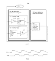
- FIG. 1 is a block diagram of an exemplary leakage inverter in accordance with one embodiment of the invention.
- FIG. 2 is a block diagram of exemplary leakage inverters with MOS components in accordance with some embodiments of the invention.
- FIG. 3 is a block diagram of an exemplary ring oscillator in accordance with one embodiment of the invention.
- FIG. 4 is a block diagram of an exemplary leakage inversion graph in accordance with one embodiment of the invention.
- FIG. 5 is a block diagram of another exemplary ring oscillator in accordance with one embodiment of the invention.
- FIG. 6 is a block diagram of an exemplary leakage inverter input control configuration in accordance with one embodiment of the invention.
- FIG. 7 is a block diagram of an exemplary leakage inverter output control configuration in accordance with one embodiment of the invention.
- FIG. 8 is a block diagram of an exemplary leakage inverter and control ring configuration in accordance with one embodiment of the invention.
- FIG. 9 is a block diagram of an exemplary delay measuring system in accordance with one embodiment of the invention.
- FIG. 10 is a block diagram of an exemplary timing diagram in accordance with one embodiment of the invention.
- FIG. 11 is a block diagram of exemplary delay measuring system in accordance with one embodiment of the invention.
- FIG. 12 is a block diagram of an exemplary Muller C-Element in accordance with one embodiment.
- FIG. 13 is a diagram of an exemplary timing graph in accordance with one embodiment of the invention.
- FIG. 14 is a block diagram of exemplary delay measuring system in accordance with one embodiment of the invention.
- FIG. 15 is a block diagram of exemplary analysis system in accordance with one embodiment of the invention.
- FIG. 16 is a block diagram of exemplary analysis system in accordance with one embodiment of the invention.
- FIG. 17 is a block diagram of exemplary analysis system in accordance with one embodiment of the invention.
- FIG. 18 is a flow chart of exemplary analysis method in accordance with one embodiment of the invention.
- FIG. 19 is a flow chart of exemplary leakage inversion process in accordance with one embodiment of the invention.
- FIG. 20 is a flow chart of exemplary analysis process in accordance with one embodiment of the invention.
- FIG. 21 is flow diagram of a method in accordance with various embodiments of the invention.
- FIG. 22 is a block diagram of iterative solving of bivariate equations to derive nodal temperature and voltage in accordance with an embodiment of the invention.
- FIG. 23 is a flow diagram of a method in accordance with various embodiments of the invention for calibrating for intra-die process variations (PV).
- PV intra-die process variations
- FIG. 24 is a block diagram of an exemplary standard ring oscillator in accordance with one embodiment of the invention.
- leakage inversion outputs can be utilized in detecting transition delays that are utilized to analyze a variety of concerns.
- the leakage inversion outputs can be utilized to analyze manufacturing process compliance and defects.
- output(s) from one or more leakage ring oscillators can be utilized to determine the temperature at the location(s) of the one or more leakage ring oscillators during operation of a chip that includes the one or more leakage ring oscillators.
- a leakage ring oscillator is located in close proximity to a standard ring oscillator, and output from the leakage ring oscillator and output from the standard ring oscillator can be utilized together to determine the temperature and voltage at the location of the leakage and standard ring oscillators during operation of a chip that includes these two types of ring oscillators.
- multiple pairs of a leakage ring oscillator and a standard ring oscillator can be implemented in multiple locations of a die or chip to determine the temperature and voltage at those multiple locations during the operation of the die or chip.
- FIG. 1 is a block diagram of an exemplary leakage inverter 100 in accordance with one embodiment of the invention.
- Leakage inverter 100 comprises a pull up component 110 , leakage component 120 and pull down component 130 .
- leakage component 120 is coupled in series between the pull up component 110 and the pull down component 130 .
- the components of leakage inverter 100 cooperatively operate to pull up and pull down a signal.
- pull up component 110 is configurable to perform a pull up operation to pull up a signal
- pull down component 130 is configurable to perform a pull down operation to pull down the signal
- a leakage in leakage component 120 impacts at least one transition of the signal.
- a transition delay associated with the pull down operation is asymmetric with respect to transition delay associated with the pull up operation and the asymmetry is associated with an effect of the leakage current on the at least one transition of the signal.
- the at least one transition of the signal is represented by graph 140 with a relatively fast rising transition delay 141 and a relatively slow transition delay 142 .
- the at least one transition of the signal is represented by graph 150 with a relatively slow rising transition delay 151 and a relatively fast transition delay 152 .
- pull up component 110 , leakage component 120 and pull down component 130 can include a variety of components.
- the leakage component includes a transistor in the off state that allows leakage current to flow.
- FIG. 2 is a block diagram of exemplary leakage inverters with MOS components in accordance with some embodiments of the invention. It is appreciated there are a variety of other leakage inverter configurations.
- Leakage inverter 210 includes a NMOS leakage transistor 212 and leakage inverter 220 includes a PMOS leakage transistor 222 .
- Leakage inverter 210 includes pull up component PMOS transistor 211 , leakage component NMOS leakage transistor 212 and pull down component NMOS transistor 213 .
- the incoming signal is low and pull down component NMOS transistor 213 turns off, pull up component PMOS transistor 211 turns on to perform a pull up operation and leakage component NMOS transistor 212 does not impact an output signal transition to a pulled up value.
- the incoming signal is high and pull up component PMOS transistor 211 turns off, pull down component NMOS transistor 213 turns on to perform a pull down operation but leakage component NMOS transistor 212 impacts the output signal transition.
- leakage inverter 210 As leakage component NMOS transistor 212 is off the pull down transition delay corresponds to a delay for leakage current and corresponding pull down value to “propagate” through the leakage component NMOS transistor 212 .
- the operations of leakage inverter 210 are represented by graph 214 with a relatively fast rising transition delay 217 and a relatively slow falling transition delay 219 .
- Leakage inverter 220 includes pull up component PMOS transistor 221 , leakage component PMOS leakage transistor 222 and pull down component NMOS transistor 223 .
- the incoming signal is high and pull up component PMOS transistor 221 turns off, pull down component NMOS transistor 223 turns on to perform a pull down operation and leakage component PMOS transistor 222 does not impact an output signal transition to a pulled down value.
- the incoming signal is low and pull down component NMOS transistor 223 turns off, pull up component PMOS transistor 221 turns on to perform a pull up operation but leakage component PMOS transistor 222 impacts the output signal transition.
- leakage inverter 220 As leakage component PMOS transistor 222 is off the pull down transition delay corresponds to a delay for leakage current and corresponding pull up value to “propagate” through the leakage component PMOS transistor 222 .
- the operations of leakage inverter 220 are represented by graph 224 with a relatively slow rising transition delay 227 and a relatively fast falling transition delay 229 .
- a leakage inverter can be included in a variety of component configurations.
- the leakage inverter can be included in a ring configuration.
- the ring oscillator includes at least one leakage inverter configured to transition a signal, wherein a leakage current impacts a transition of the signal and the at least one leakage inverter is coupled as part of a ring path.
- the at least one leakage inverter can include a leakage component coupled in series between a pull up component and a pull down component, wherein leakage in the leakage component impacts at least one transition.
- the at least one leakage inverter can have a rising transition delay and a falling transition delay that are asymmetric.
- the ring oscillator can include an output including an indication of a transition delay in the signal and can include a control component coupled to the ring path to control a state of the signal. It is appreciated the ring oscillator can include a plurality of leakage inverters. In one exemplary implementation, at least one leakage inverter is coupled in series to another leakage inverter in the ring path.
- FIG. 3 is a block diagram of exemplary ring oscillator 300 in accordance with one embodiment of the invention.
- Ring oscillator 300 includes leakage inverters 320 and 340 , AND logic components 310 and 330 , and driven inverter 350 . The components are coupled in series in a ring path.
- Leakage inverters 320 and 340 include NMOS leakage transistors.
- oscillations include inversions of a signal state.
- Leakage inverters 320 and 340 oscillate or invert a signal state wherein at least one inversion transition is impacted by a leakage characteristic of a leakage inverter.
- the oscillation rising transitions and falling transitions have asymmetric transition delays.
- leakage inverters 320 are NMOS leakage inverters similar to leakage inverter 210 .
- the AND logic components 310 and 330 can control a signal and drive the signal to a value.
- An enable signal 303 can be used to “enable” AND control logic components 310 and 330 .
- oscillation ring 300 While the present embodiment of oscillation ring 300 is shown with the same enable signal 303 “enabling” AND logic components 310 and 330 , it is appreciated that a different respective enable signal can be used to “enable” each of the AND logic components 310 and 330 .
- Driven inverter 350 switches on and off states in response to a drive signal without impacts associated with a leakage transistor.
- Ring oscillator 300 has a split 307 in the ring path that forwards an output 304 .
- the state of output 304 is similar to the state of an input to leakage inverter 320 .
- FIG. 4 is a block diagram of exemplary leakage inversion graph 400 in accordance with one embodiment of the invention.
- the enable signal 303 is set high to “enable” the flow of information through the AND gates 310 and 320 for an output that mimics the logic value on the other input of the AND gates.
- the enabling initiates a transition to a high logic value in a signal at point 391 of the oscillating ring 300 .
- This high logic value at the input of leakage inverter 340 triggers an inverse transition or falling transition to a low logic value at point 392 of an output signal from leakage inverter 340 .
- the delay in completing a falling transition in a signal from the leakage inverter 340 is relatively long compared to rising transitions in the signal at point 391 .
- the output at point 393 of a subsequent driven inverter 350 is inverted.
- the transitions in output signal 304 mimic transitions at point 393 with a slight time shift due to propagation through AND component 310 .
- the output from leakage inverter 320 at point 394 again has relatively slow or long falling transitions and relatively fast or short rising transitions.
- FIG. 5 is a block diagram of exemplary ring oscillator 500 in accordance with one embodiment of the invention.
- Ring oscillator 500 includes leakage inverters 520 and 540 , control components 510 , 530 , and 550 . The components are coupled in series in a ring path.
- Leakage inverters 520 and 540 include PMOS leakage transistors.
- oscillations include inversions of a signal state.
- Leakage inverters 520 and 540 oscillate or invert a signal state wherein at least one inversion transition is impacted by a leakage characteristic of a leakage inverter.
- the oscillations rising transitions and falling transitions have asymmetric transition delays.
- leakage inverters 520 and 540 are PMOS leakage inverters similar to leakage inverter 220 .
- the control components 510 and 530 can control a signal and drive the signal to a value.
- control component 510 and 530 respectively include a NAND logic component with a first input coupled to an enable and an inverted second input coupled to the ring path.
- An enable signal 503 can be used to “enable” NAND control logic components 510 and 530 . It is appreciated that a different respective enable signal can be used to “enable” each of the NAND logic components 510 and 530 .
- Control component 550 includes a driven inverter that switches on and off states in response to a drive signal. The driven inverter 550 switches on and off states in response to a drive signal without impacts associated with a leakage transistor.
- Ring oscillator 500 has a split 507 in the ring path that forwards an output 504 . The state of output 504 is similar to the state of an input to leakage inverter 520 .
- FIG. 6 is a block diagram of an exemplary leakage inverter input control configuration 600 in accordance with one embodiment of the invention.
- Leakage inverter input control configuration 600 includes control component 610 and leakage inverter 620 .
- Control component 610 controls the input to leakage inverter 620 .
- control component 610 can control the input to leakage inverter 620 in a variety of ways.
- Control component 610 can include a variety of different components (e.g., logic gates, on/off driven inverters, etc.).
- Control component 610 can control a state (e.g., logical value, high/low voltage, etc.) of an input to leakage inverter 620 .
- Control component 610 can control a timing (e.g., synchronize with other inputs, trigger based upon an enable, etc) of an input to leakage inverter 620 .
- FIG. 7 is a block diagram of an exemplary leakage inverter output control configuration 700 in accordance with one embodiment of the invention.
- Leakage inverter output control configuration 700 includes control component 710 and leakage inverter 720 .
- Control component 710 controls the output from leakage inverter 720 . It is appreciated that control component 710 can control the output from leakage inverter 720 in a variety of ways. Control component 710 can control a state (e.g., logical value, high/low voltage, etc.) of an output from leakage inverter 720 . Control component 710 can control a timing (e.g., synchronize with other outputs, trigger based upon an enable, etc) of an output from leakage inverter 720 .
- a state e.g., logical value, high/low voltage, etc.
- Timing e.g., synchronize with other outputs, trigger based upon an enable, etc
- FIG. 8 is a block diagram of an exemplary leakage inverter and control ring configuration 800 in accordance with one embodiment of the invention.
- Control ring configuration 800 includes control components (e.g., 811 , 812 and 813 ) and leakage inverters (e.g., 821 and 822 ).
- Control components 811 , 812 and 813 can be utilized to implement a variety of different type of controls (e.g., state determination, timing, etc.). It is appreciated that control components 811 , 812 and 813 can receive control inputs (e.g., enables, triggers, etc.) that direct the control.
- control component 811 receives control input 809 .
- control components 811 and 812 include logic gates (e.g., similar 310 , 330 , 510 , 530 , etc.) and control component 813 includes an on/off driven inverter (e.g., similar to 350 , 550 , etc.).
- the leakage inversion stage can be a leakage starving stage that is not necessarily inverter. In one embodiment, instead of having just one of the stages gated it can have basically both of them gated. In one exemplary implementation both N and P would be gated with a leakage device. There can be a really tiny generalization as a leakage current starved inverter. There can be a drive inverter and a pass gate that is off, like a tri-state inverter that is off essentially.
- a signal transition delay is measured.
- the transition delay can correspond to a delay from the initiation of an inversion transition to the completion of the inversion transition.
- the transition delays can be asymmetric and an amount of time to complete a pull up or rising transition can be different from an amount of time to complete a pull down or falling transition (e.g., fast rising transition versus slow falling transition, vise versa, etc.).
- the measurement can be associated with an isolated or particular transition direction (e.g., measurement of delay associated with a slow falling transition distinct from delay associated with a fast rising transition, vise versa, etc.).
- the delays can be introduced by a variety of operations (e.g., delay associated with a regular pull up operation versus with waiting for leakage conditions on a pull down operation, delay associated with a pre-charge operation versus a read operation, etc.).
- the indication of delay measurements can be utilized in a variety of different analysis (e.g., analyze manufacturing process compliance and defects, leakage current power consumption, etc.).
- the analysis process can include analyzing a fabrication process and operating parameters based upon the amount of delay time associated with a transition.
- the analysis process can include determining the temperature at the location(s) of the one or more leakage ring oscillators during operation of a chip that includes the one or more leakage ring oscillators.
- a leakage ring oscillator is located in close proximity to a standard ring oscillator, and the analysis process can be utilized to determine the temperature and voltage at the location of the leakage ring oscillator and standard ring oscillator during operation of a chip that includes the leakage ring oscillator and standard ring oscillator.
- multiple pairs of a leakage ring oscillator and a standard ring oscillator can be implemented in multiple locations of a die or chip and the analysis process can include determining the temperature and voltage at those multiple locations during the operation of the die or chip.
- FIG. 9 is a block diagram of exemplary delay measuring system 900 in accordance with one embodiment of the invention.
- Delay measuring system 900 includes a first transition stage 910 , a second transition stage 920 , and a transition completion detection component 930 .
- the first transition stage 910 and the second transition stage 920 are parallel to one another and included in a ring configuration with the transition completion detection component 930 .
- the first transition stage 910 includes a first component under test 911 and driven inverter 912 and the first transition stage 910 is operable to cause at least one inversion transition.
- the second transition stage 920 includes a second component under test 921 and driven inverter 922 and the second transition stage 920 is operable to cause at least one inversion transition.
- the transition completion detection component 930 is coupled to the first component under test 911 and the second component under test 921 .
- the transition completion detection component 930 is operable to detect an indication of the amount of delay time from initiating an inversion transition to completing the inversion transition. It is appreciated components of exemplary delay measuring system 900 can include a variety of different configurations. Additional different exemplary delay measuring system configurations and components are described in later sections of the present description.
- the indication of the amount of delay time can be based upon the output of the transition completion detection device and can be directed to one aspect (e.g., pull up versus pull down, rising transition versus falling transition, etc.) of an asymmetric delay.
- the indication of a transition delay can isolate delays associated with transitions in one direction (e.g., pull up, rising, etc.) from delays associated with transitions in another direction (e.g., pull down, falling, etc.), or vice versa.
- FIG. 10 is a block diagram of an exemplary timing diagram of a count of slow falling transitions in accordance with one embodiment of the invention.
- the rising edges of the count signal 1020 are associated with the slow falling transitions of the transition completion detection device output signal 1010 .
- the count of the slow falling transitions can be utilized to determine a slow falling transition delay time or time to complete the slow falling transition. It is appreciated that isolated indication or measurement of a transition delay associated with one transition direction can be utilized to refine examination and analysis of characteristics and features associated with the components under test. Additional description of examination and analysis of characteristics and features associated with the components under test is set forth in later sections.
- Transitions stage 910 and 920 can include pull up components and pull down components.
- a component under test can cause a transition itself or impact (e.g., delay, alter, etc.) a transition from another component.
- the component under test 911 and component under test 921 can be inverters.
- An inverter can be a leakage inverter and have a transition delay that is primarily a function of the leakage current.
- the outputs of the transition stages can be inverted whether or not the component under test 911 and component under test 921 themselves invert their respective inputs.
- the transition stages can include an inverter with a transition delay that is primarily a function of drive current (e.g., saturation current, on current, etc.).
- FIG. 11 is a block diagram of exemplary delay measuring system 1100 in accordance with one embodiment of the invention.
- the components under test in delay measuring system 1100 are leakage inverters.
- Delay measuring system 1100 includes first transition stage 1110 , second transition stage 1120 , transition completion detection component 1130 and control component 1150 .
- Transition stage 1110 includes leakage inverter 1111 and driven inverter 1112 .
- Transition stage 1120 includes leakage inverter 1121 and driven inverter 1122 .
- Transition completion detection component 1130 includes C-Element 1131 and driven inverter 1132 .
- leakage inverters 1111 and 1121 are configured to transition a signal, wherein a leakage current impacts a transition of the signal.
- the leakage current characteristic impacts a transition delay (e.g., a delay from beginning a transition to completing the transition, etc.). The impact can include delaying the transition.
- the leakage current characteristic can impact the rising or pull up transition delay or the falling of pull down transition delay.
- Leakage inverters can be similar to leakage inversion components and systems described in co-pending Applications entitled “A System And Method For Examining Leakage Impacts” (U.S. patent application Ser. No. 13/287,044) and “A System And Method For Examining Asymmetric Operations” (U.S. patent application Ser. No. 13/287,053), both of which are incorporated herein by reference.
- FIG. 12 is a block diagram of an exemplary Muller C-Element 1200 in accordance with one embodiment.
- Muller C-Element 1200 includes NAND logic components 1230 and 1240 , OR logic gates 1210 and 1220 . The inputs to OR logic gate 1210 are inverted.
- Muller C-Element 1200 has two inputs and one output.
- Muller C-Element 1200 is operable: to output a logical 0 if the two inputs are both a logical 0 and continue to output a logical 0 until the two inputs are a logical 1; to output a logical 1 if the two inputs are both a logical 1 and continue to output a logical 1 until the two inputs are a logical 0.
- the output does not change if: both inputs are a logical 0 and only one of the inputs changes to a logical 1; or both inputs are a logical 1 and only one of the inputs changes to a logical 0.
- FIG. 13 is a diagram of exemplary timing graph 1300 in accordance with one embodiment of the invention.
- Timing graph 1300 corresponds to one exemplary implementation of delay measuring system 1100 and illustrates respective signal transitions at points 1171 , 1172 , 1173 , 1174 , 1175 , 1177 , 1178 and 1179 .
- FIG. 14 is a block diagram of exemplary delay measuring system 1400 in accordance with one embodiment of the invention.
- the components of delay measuring system 1400 are similar to an embodiment of delay measuring system 1100 when NMOS leakage inverters are the components under test.
- Delay measuring system 1400 includes first transition stage 1410 , second transition stage 1420 , transition completion detection component 1430 and control component 1450 .
- Transition stage 1410 includes leakage inverter 1411 and driven inverter 1412 .
- Transition stage 1420 includes leakage inverter 1421 and driven inverter 1422 .
- Transition completion detection component 1430 includes C-Element 1431 and driven inverter 1432 .
- leakage inverter 1411 and leakage inverter 1421 include NMOS leakage inverters similar to NMOS leakage inverter 1410 and C-Element 1431 includes a C-Element similar to C-Element 1200 .
- FIG. 15 is a block diagram of exemplary analysis system 1500 in accordance with one embodiment of the invention.
- Analysis system 1500 includes leakage inversion component 1510 and analysis component 1520 .
- the leakage inversion component 1510 can include a variety of leakage inversion implementations.
- Leakage inversion component 1510 can include at least one leakage inverter (e.g., 100 , 210 , 220 , etc.).
- Leakage inversion component 1510 can include at least one control component (e.g., 310 , 510 , 610 , 710 , etc.).
- analysis component 1520 can include a variety of implementations.
- the analysis component 1520 can include components on chip with the leakage inversion component, components off chip from the leakage inversion component, combination of components on and off chip. It is also appreciated that the analysis component 1520 can perform a variety of different analysis. In one exemplary implementation, the analysis can include transition delays, determination of leakage power consumption, manufacturing process compliance and defects, etc.
- FIG. 16 is a block diagram of exemplary analysis system 1600 in accordance with one embodiment of the invention.
- Analysis system 1600 includes leakage inversion component 1610 and analysis component 1620 .
- Leakage inversion component 1610 includes a leakage oscillating ring comprising AND gates 1611 and 1613 , leakage inverters 1612 and 1614 , and on/off driven inverter 1615 coupled in a ring path.
- Output 1604 is forwarded from leakage inversion component 1610 to analysis component 1620 .
- Analysis component 1620 includes counter 1621 and processing component 1622 .
- FIG. 17 is a block diagram of exemplary analysis system 1700 in accordance with one embodiment of the invention.
- Analysis system 1700 includes delay measuring component or system 1710 and analysis component 1720 .
- Delay measuring system 1710 includes a first transition stage 1713 , a second transition stage 1714 , a transition completion detection component 1715 and control component 1711 .
- the first transition stage 1713 includes a first component under test 1731 and driven inverter 1732 .
- the second transition stage 1714 includes a second component under test 1741 and driven inverter 1742 .
- Transition completion detection component 1715 includes C-element 1751 and driven inverter 1752 .
- the components of delay measuring system 1710 are similar to components of delay measuring system 900 .
- Analysis component 1720 performs analysis based upon the output 1704 from delay measuring system 1710 . In one embodiment analysis component 1720 performs an analysis process similar to an analysis process of block 1820 .
- an analysis is directed to other aspects beyond leakage current.
- the analysis is more concerned with a related but different characteristic. The concern or examination can be directed to what the static power consumption of the device is. It is appreciated there is a lot of analysis that can be done while examining the delay in the frequency.
- component configurations and operations are simulated in spice and then compared to the measured result with present systems. If the physical implementation is running faster than the simulated version then there is an indication the leakage is higher than expected.
- the difference between the PMOS and NMOS leakage is analyzed. This is similar to asymmetric situations.
- ring oscillator One thing that was previously extremely challenging in terms of ring oscillator is how to figure out how much of a characteristic (e.g., delay, power consumption, etc.) is associated with or attributable to NMOS components and how much is associated with or attributable to PMOS components.
- a characteristic e.g., delay, power consumption, etc.
- present systems and methods can be implemented in a variety of situations or environments.
- Present systems and methods can facilitate confirmation of chip compliance with design specifications and detection of manufacturing process irregularities.
- Present systems and methods can facilitate examination and analysis of asymmetric characteristics.
- the output of present systems can include a waveform that is acceptable to a counter.
- a frequency and duty cycle can be determined by a fast transition.
- the present operation examination approaches facilitate utilization of relatively small ring oscillations with asymmetric delay devices that achieve proper polarities.
- present approaches can also allow for measurement and analysis components (e.g., components of systems 100 , 300 , 800 , 1300 , etc.) to be selectively turned on and off facilitating further conservation of power consumption.
- the present approaches facilitate more monitoring structures to be instantiated than conventional attempts and at a lower area cost.
- the present approaches also facilitate closer monitoring of process and operating parameters.
- present systems and methods can facilitate determining the temperature at the location(s) of the one or more leakage ring oscillators during operation of a chip that includes the one or more leakage ring oscillators.
- present systems and methods can facilitate determining the temperature and voltage at the location of a leakage ring oscillator and a standard ring oscillator during operation of a chip that includes the leakage ring oscillator and standard ring oscillator.
- multiple pairs of a leakage ring oscillator and a standard ring oscillator can be implemented in multiple locations of a die or chip and present systems and methods can facilitate determining the temperature and voltage at those multiple locations during the operation of the die or chip.
- FIG. 18 is a flow chart of exemplary analysis method 1800 in accordance with one embodiment of the invention.
- a leakage inversion process is performed.
- the leakage inversion process includes pull ups and pull downs wherein at least one transition is impacted by leakage characteristics.
- the leakage inversion process includes transitions between a logical 1 state to a logical 0 state.
- an analysis process is performed based upon the leakage inversion process. It is appreciated that a variety of different analysis can be performed.
- transitions delays are utilized in determining a frequency and the frequency can be converted back to an indication of a leakage current determination.
- the leakage inverter gate capacitance is known and an RC (resistance/capacitance) delay can be utilized to determine the current.
- a frequency division or adjustment can be a function of the number of inverters in the ring.
- the frequency can be utilized for determining the temperature at the locations of the ring oscillator during operation of a chip.
- the frequency can be utilized for determining the temperature and voltage at the location of the leakage and standard ring oscillators during operation of a chip that includes these two types of ring oscillators.
- results from a ring oscillator including a leakage inverter are compared to a spice simulation of the circuit. If the actual physical implementation is running faster then it is an indication the leakage is higher than expected.
- results from a ring oscillator including a leakage inverter can be utilized to determine the temperature at the locations of the ring oscillator during operation of a chip that includes the ring oscillator.
- a ring oscillator including a leakage inverter is located in close proximity to a standard ring oscillator, and results from the leakage ring oscillator and results from the standard ring oscillator can be utilized together to determine the temperature and voltage at the location of the leakage ring oscillator and standard ring oscillator during operation of a chip that includes the leakage ring oscillator and standard ring oscillator.
- multiple pairs of a ring oscillator including a leakage inverter (leakage ring oscillator) and a standard ring oscillator can be implemented in multiple locations of a die or chip to determine the temperature and voltage at those multiple locations during the operation of the die or chip.
- a simulation is performed in which the device under test or leakage inverts is replaced with a current source in the simulation and currents that is put in the source is swept through various values. In one exemplary implementation, the values are swept until the frequency matches what is being measured and that can be utilized as an indication of what the current is on those leakage devices. In one exemplary implementation, characteristics of a leakage inverter on silicon is compared to a simulated ideal current source. In one exemplary implementation, the output of the simulated current source is charted or graphed versus frequency and if the current is high then frequency is high. The graph can be used to compare a measured frequency of a leakage inversion component to an ideal graph simulation. The simulation graph can be utilized to do the correlation between frequency and current.
- FIG. 19 is a flow chart of exemplary leakage inversion process 1900 in accordance with one embodiment of the invention.
- leakage inversion process 1900 is similar to the leakage inversion process of block 1810 .
- a signal in a first state is received.
- the signal can be a first logical state signal (e.g., a characteristic of the signal corresponds to a first logical state, etc.).
- the first logic state signal can correspond to a logical 1.
- the first logic state signal can correspond to a logical 0.
- the first logic state signal can correspond to a pulled up or high voltage signal.
- the first logic state signal can correspond to a pulled down or low voltage signal.
- a characteristic of at least one component is changed.
- the component is a transistor and a characteristic of the at least one transistor is changed.
- the transistor can be a pull up transistor or a pull down transistor. Changing the characteristic of the transistor can turn the transistor on or off.
- a voltage value at a gate of the transistor and a characteristic e.g., resistance of a channel, etc. is changed to turn on or off the transistor.
- the change in the component inverts the logical value of a signal.
- a signal in a second state is output, wherein a delay between receiving the first logical state signal and outputting the second logical state signal is impacted by a leakage current.
- the signal can be a second logic state signal.
- the second logic state is the opposite or inverse of the first logic state.
- the first logical state is a logical 1 and the second logical state is a logical 0.
- the first logical state is a logical 0 and the second logical state is a logical 1.
- a leakage current increases or makes the delay longer than would otherwise take if the leakage current was not impacting the transition.
- FIG. 20 is a flow chart of exemplary analysis process 2000 in accordance with one embodiment of the invention.
- analysis process 2000 is similar to the analysis process of block 1820 .
- an indication associated with a leakage characteristic is received.
- the indication includes transitions in a signal in which at least one transition delay is impacted by a leakage characteristic.
- a transition delay time is determined, wherein the transition delay time is impacted by a leakage characteristic.
- characteristics of a device are analyzed based upon the transition delay time. It is appreciated that a variety of characteristics can be analyzed.
- output(s) from one or more leakage ring oscillators can be utilized to determine the temperature at the location(s) of the one or more leakage ring oscillators during operation of a chip that includes the one or more leakage ring oscillators.
- a leakage ring oscillator is located in close proximity to a standard ring oscillator, and output from the leakage ring oscillator and output from the standard ring oscillator can be utilized together to determine the temperature and voltage at the location of the leakage ring oscillator and standard ring oscillator during operation of a chip that includes the leakage ring oscillator and standard ring oscillator.
- multiple pairs of a leakage ring oscillator and a standard ring oscillator can be implemented in multiple locations of a die or chip to determine the temperature and voltage at those multiple locations during the operation of the die or chip.
- FIG. 21 is a flow diagram of a method 2100 in accordance with various embodiments of the invention for determining temperature and voltage at a location of a die or semiconductor device. Although specific operations are disclosed in FIG. 21 , such operations are examples. The method 2100 may not include all of the operations illustrated by FIG. 21 . Also, method 2100 may include various other operations and/or variations of the operations shown. Likewise, the sequence of the operations of flow diagram 2100 can be modified. It is appreciated that not all of the operations in flow diagram 2100 may be performed. In various embodiments, one or more of the operations of method 2100 can be performed by software, by firmware, by hardware or by any combination thereof, but is not limited to such.
- Method 2100 can include processes of embodiments of the invention which can be performed by a processor(s) and electrical components under the control of computer or computing device readable and executable instructions (or code).
- the computer or computing device readable and executable instructions (or code) may reside, for example, in data storage features such as computer or computing device usable volatile memory, computer or computing device usable non-volatile memory, and/or computer or computing device usable mass data storage.
- the computer or computing device readable and executable instructions (or code) may reside in any type of computer or computing device readable medium or memory.
- method 2100 can be used to determine accurate temperature and voltage at each sensor location on a die or semiconductor device while the chip is functioning.
- time-varying thermal and voltage-droop heat-maps of the die can be created. Therefore, this information can be used to observe the hot-spot migration as well as static voltage droops on the die.
- such information can be utilized for numerous applications such as (but not limited to): implementation of efficient thermal solutions, accurate PVT (process, voltage, and temperature) evaluations, device reliability study, and the like.
- method 2100 in one embodiment is immune to voltage noise and actually computes or determines the voltage at each sensor location.
- method 2100 can be implemented as part of an analysis component (e.g., 1520 , 1620 , and/or 1720 ) as described herein, but is not limited to such.
- two types of sensors can be modeled as functions of temperature and voltage as independent variables.
- these functions are used to compute the temperature (and voltage) using the frequency value of the corresponding sensor (e.g., ring oscillator).
- the nodal temperature and voltage can be determined based on data received from the two sensors. In this manner, method 2100 can be used to determine accurate temperature and voltage at each sensor location on a die or semiconductor device while the chip is functioning.
- two types of sensors can be modeled as functions of temperature and voltage as independent variables.
- the modeling can involve the characterization of each sensor under a range of stabilized temperature and voltage conditions while a die or chip is operating. It is pointed out that operation 2102 can be implemented in a wide variety of ways.
- the two types of sensors can be placed in close proximity to each other as part of a die or semiconductor device (e.g., graphics processor unit (GPU), central processor unit (CPU), processor, microprocessor, and the like).
- a die or semiconductor device e.g., graphics processor unit (GPU), central processor unit (CPU), processor, microprocessor, and the like.
- the two sensors do not need to be right next to each other to be in close proximity.
- one of the sensors can be implemented as a ring oscillator that is sensitive to temperature while the other sensor can be implemented as a ring oscillator that is sensitive to voltage.
- the temperature sensitive ring oscillator can be implemented with a leakage ring oscillator (e.g., 100 , 300 , or 500 ) composed of specialized current-starved inverters while the voltage sensitive ring oscillator (e.g., 2400 of FIG. 24 ) can be implemented with a ring-oscillator composed of minimum sized inverters, but are not limited to such.
- the voltage sensitive ring oscillator can be implemented with a generic (or standard or normal or non-leakage) ring oscillator with an odd number of inverters.
- both the ring-oscillators may be sensitive to temperature as well as voltage, but their relative sensitivity to temperature and voltage is orthogonal in nature.
- the leakage ring-oscillator can be very sensitive to temperature and less sensitive to voltage while the other ring-oscillator can be very sensitive to voltage and less sensitive to temperature.
- process 2100 can produce a more accurate result with a lesser number of iterations.
- a temperature sensitive sensor and a voltage sensitive sensor can be implemented as a leakage ring oscillator and a standard ring oscillator, respectively.
- the frequency of the standard ring oscillator will exhibit a more dramatic change than the frequency of the leakage ring oscillator.
- the frequency of the leakage ring oscillator will exhibit a more dramatic change than the frequency of the standard ring oscillator.
- characterization can be performed of the leakage ring oscillator (e.g., 100 , 300 , or 500 ) and the standard ring oscillator (e.g., 2400 ) under a range of stabilized temperature and voltage conditions.
- a chip or die is set to a known temperature (e.g., 25° C.) and the voltage is set to a known value (e.g., 0.9 V). Then the count (or frequency) is determined of both the leakage ring oscillator and the standard ring oscillator under these conditions. Once the count for each is measured, that data can be stored by memory in association with the known temperature, voltage, and corresponding ring oscillator.
- the voltage for the chip or die can be set to another known value (e.g., 1.0 V) while keeping the temperature set at the previous value (e.g., 25° C.). Then the count (or frequency) is determined of both the leakage ring oscillator and the standard ring oscillator under these changed conditions. Once the count for each is measured, that data can be stored by memory in association with the known temperature, voltage, and corresponding ring oscillator. This process can be repeated for different voltage values. Once all the desired voltage values are done at the established (or known) temperature, then the temperature can be changed to a different value (e.g., 35° C.).
- a different value e.g. 35° C.
- this process can be performed for a desired range of temperature values in gradual steps (e.g., 25° C., 35° C., 45° C., 55° C., 65° C., . . . 105° C.) and a desired range of voltage values in gradual steps (e.g., 0.9 V, 1.0 V, . . . 1.2 V).
- the predicted count (or frequency) of the leakage ring oscillator and the predicted count (or frequency) of the standard ring oscillator are known.
- a count (or frequency) value of the leakage ring oscillator can be associated with a known temperature and/or known voltage.
- a count (or frequency) value of the standard ring oscillator can be associated with a known temperature and/or known voltage. It is noted that operation 2102 can be implemented in any manner similar to that described herein, but is not limited to such.
- a nodal temperature and voltage can be determined based on data received from the two sensors. It is noted that operation 2104 can be implemented in a wide variety of ways. For example in an embodiment, a cross-coupled model can be utilized at operation 2104 that uses data received from the two sensors and iteratively converges to actual node temperature and voltage. In one embodiment, at operation 2104 , iterative solving of bivariate equations (each representing a sensor) can be performed to derive or determine nodal temperature and voltage.
- a global trigger mechanism implemented on chip can be utilized to trigger all the sensors (e.g., the two ring oscillators) at about or substantially the same time (or at the same time) during a functional test.
- all sensors e.g., the two ring oscillators
- each of the counts of the ring-oscillators are read out at operation 2104 and translated to frequency values.
- a circuit can be implemented that performs measurements across an entire chip or die by starting and stopping all of the sensors at approximately or substantially the same time (or at the same time).
- FIG. 22 is a block diagram 2200 of iterative solving of bivariate equations (each representing a sensor) to derive nodal temperature and voltage in accordance with an embodiment of the invention.
- FIGS. 21 and 22 are described in combination in order to provide a better understanding of operation 2104 .
- a normal ring oscillator (RO) function or model 2202 and a leakage ring oscillator (RO) function or model 2204 can be implemented in a wide variety of ways.
- a wide variety of functions or formulas or equations can be utilized to model the normal ring oscillator (RO) function or model 2202 and a leakage ring oscillator (RO) function or model 2204 .
- anything can be utilized that best models the collected data (e.g., any surface function that best fits that model with the least error).
- a regression analysis can be utilized for the normal ring oscillator (RO) function or model 2202 and a leakage ring oscillator (RO) function or model 2204 .
- the standard ring oscillator model 2202 can convert the measured frequency and temperature into voltage 2206 .
- the computed voltage 2206 forms an input to the leakage ring oscillator (RO) model 2204 , which converts the measured frequency and voltage into temperature 2208 .
- this process can be repeated at operation 2104 until the computed or determined temperature 2208 and voltage 2206 converge to a static value (e.g., 0 delta between iterations), but is not limited to such. In another embodiment, this process can be repeated at operation 2104 for a finite number of iterations to computed or determine temperature 2208 and voltage 2206 , but is not limited to such. In one embodiment, note that the determined temperature 2208 and voltage 2206 have their own importance since people will look at static voltage droop as well as temperature in some applications.
- operation 2104 can be implemented as a system test of a die or chip or semiconductor device, but is not limited to such.
- the system test can include running any application (e.g., game, program, and the like) on the die or chip or semiconductor device at operation 2104 , and then determining the hottest spot or area in the die or chip or semiconductor device.
- that determined information can be utilized to enable or trigger one or more cooling solutions for the die or chip or semiconductor device.
- operation 2104 enables accurately predicting or determining the temperature at any location in the chip (or die or semiconductor device) when it is doing any function.
- Operation 2104 can be implemented in any manner similar to that described herein, but is not limited to such.
- method 2100 of FIG. 21 can be implemented to operate with any number of sensor pairs that include a temperature sensitive sensor and a voltage sensitive sensor.
- a temperature sensitive sensor and a voltage sensitive sensor are implemented as a leakage ring oscillator and a standard ring oscillator, respectively, they have the benefit of being small in size thereby enabling them to be implemented in multiple locations of a chip, die, or semiconductor device.
- the total area of a leakage ring oscillator and counter (involved in digitally measuring the frequency) in combination with a standard ring oscillator and counter (involved in digitally measuring the frequency) is multiple times smaller than the size of the thermal diode circuitry, it can be inexpensively distributed across a die or chip. Note that better understanding of chip circuitry behavior and more accurate sensing capabilities across the die or chip can enable cheaper and more efficient thermal solutions along with creating time-varying thermal and voltage-droop heat-maps of the die or chip.
- FIG. 23 is a flow diagram of a method 2300 in accordance with various embodiments of the invention for calibrating for intra-die process variations (PV). Although specific operations are disclosed in FIG. 23 , such operations are examples. The method 2300 may not include all of the operations illustrated by FIG. 23 . Also, method 2300 may include various other operations and/or variations of the operations shown. Likewise, the sequence of the operations of flow diagram 2300 can be modified. It is appreciated that not all of the operations in flow diagram 2300 may be performed. In various embodiments, one or more of the operations of method 2300 can be performed by software, by firmware, by hardware or by any combination thereof, but is not limited to such.
- Method 2300 can include processes of embodiments of the invention which can be performed by a processor(s) and electrical components under the control of computer or computing device readable and executable instructions (or code).
- the computer or computing device readable and executable instructions (or code) may reside, for example, in data storage features such as computer or computing device usable volatile memory, computer or computing device usable non-volatile memory, and/or computer or computing device usable mass data storage.
- the computer or computing device readable and executable instructions (or code) may reside in any type of computer or computing device readable medium or memory.
- a component under test (CUT) ring oscillator (RO) value can be measured at two different voltage and temperature (v,t) points.
- the measured CUT RO value at operation 2302 can be a count output by the CUT RO after a defined time period or duration.
- a first measured value (or count) of the CUT RO at a first temperature (t1) and first voltage (v1) can be represented by CUT1 while a second measured value (or count) of the CUT RO at a second temperature (t2) and second voltage (v2) can be represented by CUT2.
- a first reference value (or count) derived from a model at the first temperature (t1) and the first voltage (v1) can be represented by REF1 while a second reference value (or count) derived from the model at the second temperature (t2) and the second voltage (v2) can be represented by REF2.
- operation 2302 can be implemented in any manner similar to that described herein, but is not limited to such.
- the reference model can be transformed to derive a component under test model.
- operation 2306 can be implemented in a wide variety of ways.
- FIG. 24 is a block diagram of exemplary standard (or normal) ring oscillator 2400 in accordance with one embodiment of the invention.
- ring oscillator 2400 can be referred to as a non-leakage ring oscillator, but is not limited to such.
- Ring oscillator 2400 includes driven inverters 2420 , 2440 and 2450 , and control logic components 2410 and 2430 . The components are coupled in series in a ring path.
- Driven inverter 2420 includes an NMOS transistor and a PMOS transistor.
- oscillations include inversions of a signal state.
- Driven inverters 2420 , 2440 , and 2450 switch on and off states in response to a drive signal.
- the control logic components 2410 and 2430 can control a signal and drive the signal to a value.
- An enable signal 2403 can be used to “enable” control logic components 2410 and 2430 . While the present embodiment of oscillation ring 2400 is shown with the same enable signal 2403 “enabling” logic components 2410 and 2430 , it is appreciated that a different respective enable signal can be used to “enable” each of the logic components 2410 and 2430 .
- Driven inverter 2450 switches on and off states in response to a drive signal.
- Ring oscillator has a split 2407 in the ring path that forwards an output 2404 .
- the state of output 2404 is similar to the state of an input to inverter 2420 .
- a leakage sensitive ring oscillator (e.g. 100 , 300 , or 500 ) can be implemented that exhibits extreme temperature sensitivity and can be implemented in an area 100 times smaller than a thermal diode and corresponding circuitry.
- the leakage ring oscillator (e.g. 100 , 300 , or 500 ) can consists of a skewed leakage current limited inverter and a C-element ring oscillator design as described herein, but is not limited to such.
- either the pull down current or delay can be limited by the leakage current of an OFF NMOS device in the NLEAK inverter or the pull up current or delay can be limited by the leakage current of an OFF PMOS device in a PLEAK inverter.
- the leakage current limited delay is so large it dominates the ring oscillator frequency, which can be digitally measured with a counter. Since leakage current has a very strong dependence on temperature and is relatively insensitive to voltage, this type of leakage ring oscillator can serve as an excellent temperature sensor in accordance with various embodiments.
- the total area of the leakage ring oscillator and counter involved in digitally measuring the frequency is 100 times smaller than the size of the thermal diode circuitry, it can be inexpensively distributed across the chip. Note that better understanding of chip circuitry behavior and more accurate sensing capabilities across the chip can enable cheaper and more efficient thermal solutions. In addition, this can directly translate to lower board cost and higher performance per watt.
- Present systems and methods can facilitate examination and analysis of leakage characteristics.
- the leakage current limited delay is so large it dominates the ring oscillator frequency, which can be digitally measured with a counter.
- the present operation examination approaches facilitate utilization of relatively small ring oscillations with asymmetric delay devices that achieve proper polarities.
- the present approaches can also allow for operation examination components to be selectively turned on and off facilitating further conservation of power consumption.
- the present approaches facilitate more monitoring structures to be instantiated than conventional attempts and at a lower area cost.
- the present approaches also facilitate closer monitoring of process and operating parameters.
- output(s) from one or more leakage ring oscillators can be utilized to determine the temperature at the location(s) of the one or more leakage ring oscillators during operation of a chip.
- a leakage ring oscillator is located in close proximity to a standard ring oscillator, and output from the leakage ring oscillator and output from the standard ring oscillator can be utilized together to determine the temperature and voltage at the location of the leakage ring oscillator and standard ring oscillator during operation of a chip.
- program modules include routines, programs, objects, components, data structures, etc., that perform particular tasks or implement particular abstract data types.
- functionality of the program modules may be combined or distributed as desired in various embodiments.
Abstract
Description
L RO =f L(T,v)=a 0 +a 1 T+a 2 v+a 3 Tv+a 4 T 2 +a 5 v 2 +a 6 T 2 v+a 7 Tv 2
and the normal (or standard) ring oscillator (RO) function or
S RO =f N(V,t)=a 0 +a 1 t+a 2 V+a 3 tV+a 4 t 2 +a 5 V 2 +a 6 t 2 V+a 7 tV 2
L RO =f L(T,v)=A 0 T+A 1 v+A 2 T 2 +A 3 V 2 +A 4 Tv . . .
and the normal (or standard) ring oscillator (RO) function or
S RO =f N(V,t)=A 0 t+A 1 V+A 2 t 2 +A 3 V 2 +A 4 tV . . .
m=(CUT2−CUT1)/(REF2−REF1) b=CUT2−m*REF2
wherein CUT1, CUT2, REF1, and REF2 are defined above with reference to
RO CUT(t,v)=m*RO REF(t,v)+b
wherein m and b are defined above with reference to
Claims (20)
Priority Applications (4)
| Application Number | Priority Date | Filing Date | Title |
|---|---|---|---|
| US13/358,387 US9448125B2 (en) | 2011-11-01 | 2012-01-25 | Determining on-chip voltage and temperature |
| DE102012219971.3A DE102012219971B4 (en) | 2011-11-01 | 2012-10-31 | Determine on-chip voltage and temperature |
| CN201210431977.XA CN103091619B (en) | 2011-11-01 | 2012-11-01 | Determine On-chip Voltage And Temperature |
| TW101140486A TWI527193B (en) | 2011-11-01 | 2012-11-01 | Method and system of determining on-chip voltage and temperature |
Applications Claiming Priority (4)
| Application Number | Priority Date | Filing Date | Title |
|---|---|---|---|
| US201161554490P | 2011-11-01 | 2011-11-01 | |
| US13/287,044 US20130106524A1 (en) | 2011-11-01 | 2011-11-01 | System and method for examining leakage impacts |
| US13/287,053 US8952705B2 (en) | 2011-11-01 | 2011-11-01 | System and method for examining asymetric operations |
| US13/358,387 US9448125B2 (en) | 2011-11-01 | 2012-01-25 | Determining on-chip voltage and temperature |
Publications (2)
| Publication Number | Publication Date |
|---|---|
| US20130110437A1 US20130110437A1 (en) | 2013-05-02 |
| US9448125B2 true US9448125B2 (en) | 2016-09-20 |
Family
ID=48084632
Family Applications (1)
| Application Number | Title | Priority Date | Filing Date |
|---|---|---|---|
| US13/358,387 Active 2034-04-13 US9448125B2 (en) | 2011-11-01 | 2012-01-25 | Determining on-chip voltage and temperature |
Country Status (4)
| Country | Link |
|---|---|
| US (1) | US9448125B2 (en) |
| CN (1) | CN103091619B (en) |
| DE (1) | DE102012219971B4 (en) |
| TW (1) | TWI527193B (en) |
Cited By (4)
| Publication number | Priority date | Publication date | Assignee | Title |
|---|---|---|---|---|
| US20190245539A1 (en) * | 2013-09-12 | 2019-08-08 | Micron Technology, Inc. | Apparatus and methods for leakage current reduction in integrated circuits |
| US10664027B2 (en) * | 2018-10-09 | 2020-05-26 | Intel Corporation | Methods, systems and apparatus for dynamic temperature aware functional safety |
| EP3560101A4 (en) * | 2016-12-23 | 2020-08-19 | ATI Technologies ULC | Adaptive oscillator for clock generation |
| US11313900B2 (en) | 2020-08-24 | 2022-04-26 | Stmicroelectronics International N.V. | Methods and devices for measuring leakage current |
Families Citing this family (23)
| Publication number | Priority date | Publication date | Assignee | Title |
|---|---|---|---|---|
| DE112012003071T5 (en) | 2011-07-22 | 2014-04-10 | Nvidia Corporation | Component analysis systems and methods |
| US9425772B2 (en) | 2011-07-27 | 2016-08-23 | Nvidia Corporation | Coupling resistance and capacitance analysis systems and methods |
| US8952705B2 (en) | 2011-11-01 | 2015-02-10 | Nvidia Corporation | System and method for examining asymetric operations |
| CN103983809A (en) | 2013-02-08 | 2014-08-13 | 辉达公司 | PCB and online testing structure thereof, and manufacturing method of online testing structure |
| US9442025B2 (en) | 2013-10-30 | 2016-09-13 | Apple Inc. | System and method for calibrating temperatures sensor for integrated circuits |
| TWI512422B (en) * | 2014-10-14 | 2015-12-11 | Univ Nat Sun Yat Sen | Output buffer with pvtl compensation and the leakage compensation circuit thereof |
| TW201708835A (en) | 2015-08-04 | 2017-03-01 | 財團法人工業技術研究院 | System for monitoring an electronic circuit and a method for monitoring an electronic circuit |
| US9720033B2 (en) * | 2015-09-29 | 2017-08-01 | Apple Inc. | On-chip parameter measurement |
| US9825620B2 (en) | 2016-01-21 | 2017-11-21 | Apple Inc. | Method and apparatus for digital undervoltage detection and control |
| WO2018100881A1 (en) * | 2016-11-29 | 2018-06-07 | 東京エレクトロン株式会社 | Placement stand and electronic device inspecting apparatus |
| TWM542163U (en) * | 2017-01-16 | 2017-05-21 | Evga Corp | Simulation switch device of computer control chip |
| TWI806927B (en) | 2017-11-15 | 2023-07-01 | 以色列商普騰泰克斯有限公司 | Integrated circuit margin measurement and failure prediction device |
| EP3714280A4 (en) | 2017-11-23 | 2021-08-18 | Proteantecs Ltd. | Integrated circuit pad failure detection |
| US11740281B2 (en) | 2018-01-08 | 2023-08-29 | Proteantecs Ltd. | Integrated circuit degradation estimation and time-of-failure prediction using workload and margin sensing |
| TWI813615B (en) | 2018-01-08 | 2023-09-01 | 以色列商普騰泰克斯有限公司 | Integrated circuit workload, temperature and/or sub-threshold leakage sensor |
| TWI828676B (en) | 2018-04-16 | 2024-01-11 | 以色列商普騰泰克斯有限公司 | Methods for integrated circuit profiling and anomaly detection and relevant computer program products |
| US11132485B2 (en) | 2018-06-19 | 2021-09-28 | Proteantecs Ltd. | Efficient integrated circuit simulation and testing |
| WO2020141516A1 (en) | 2018-12-30 | 2020-07-09 | Proteantecs Ltd. | Integrated circuit i/o integrity and degradation monitoring |
| WO2021111444A1 (en) | 2019-12-04 | 2021-06-10 | Proteantecs Ltd. | Memory device degradation monitoring |
| EP4139697A1 (en) | 2020-04-20 | 2023-03-01 | Proteantecs Ltd. | Die-to-die connectivity monitoring |
| US11815551B1 (en) | 2022-06-07 | 2023-11-14 | Proteantecs Ltd. | Die-to-die connectivity monitoring using a clocked receiver |
| CN116087756B (en) * | 2023-03-06 | 2023-06-23 | 瀚博半导体(上海)有限公司 | Chip voltage detection method and device based on digital ring oscillator |
| TWI823812B (en) * | 2023-04-25 | 2023-11-21 | 慧榮科技股份有限公司 | Interface circuit, memory controller and calibration method thereof |
Citations (58)
| Publication number | Priority date | Publication date | Assignee | Title |
|---|---|---|---|---|
| US4922140A (en) | 1988-03-31 | 1990-05-01 | Deutsche Itt Industries Gmbh | CMOS/NMOS integrated circuit with supply voltage delay variation compensation |
| US5553276A (en) | 1993-06-30 | 1996-09-03 | International Business Machines Corporation | Self-time processor with dynamic clock generator having plurality of tracking elements for outputting sequencing signals to functional units |
| US5835553A (en) | 1995-04-20 | 1998-11-10 | Nec Corporation | Semiconductor integrated circuit having a digital temperature sensor circuit |
| US5973507A (en) | 1995-06-13 | 1999-10-26 | Fujitsu Limited | Exclusive-or gate for use in delay using transmission gate circuitry |
| US6023430A (en) | 1997-12-17 | 2000-02-08 | Nec Corporation | Semiconductor memory device asynchronously communicable with external device and asynchronous access controller for data access |
| KR20010035660A (en) | 1999-10-01 | 2001-05-07 | 김영환 | A method of measuring delay time due to interconnections |
| US6242960B1 (en) | 1999-04-08 | 2001-06-05 | Samsung Electronics Co., Ltd. | Internal clock signal generating circuit employing pulse generator |
| US6401018B1 (en) | 1999-12-24 | 2002-06-04 | Denso Corporation | Sensor device having malfunction detector |
| US20030001185A1 (en) | 2001-06-29 | 2003-01-02 | Bernhard Sell | Circuit configuration and method for determining a time constant of a storage capacitor of a memory cell in a semiconductor memory |
| US20030034848A1 (en) * | 2001-08-15 | 2003-02-20 | Norman Robert D. | Ring oscillator dynamic adjustments for auto calibration |
| US6535071B2 (en) | 2001-05-17 | 2003-03-18 | Micron Technology, Inc. | CMOS voltage controlled phase shift oscillator |
| US6535013B2 (en) | 2000-12-28 | 2003-03-18 | Intel Corporation | Parameter variation probing technique |
| TW200403779A (en) | 2002-08-27 | 2004-03-01 | Taiwan Semiconductor Mfg | Method for evaluating interconnect structure layout and the metal sheet resistance |
| US6724225B2 (en) | 2001-06-07 | 2004-04-20 | Ibm Corporation | Logic circuit for true and complement signal generator |
| TW200419688A (en) | 2003-03-31 | 2004-10-01 | Macronix Int Co Ltd | Inkless wafer test method |
| US6801096B1 (en) | 2003-01-22 | 2004-10-05 | Advanced Micro Devices, Inc. | Ring oscillator with embedded scatterometry grate array |
| US20050007154A1 (en) | 2003-07-07 | 2005-01-13 | Patella Benjamin J. | System and method for evaluating the speed of a circuit |
| US20050012556A1 (en) | 2003-07-18 | 2005-01-20 | International Business Machines Corporation | Method and apparatus for determining characteristics of MOS devices |
| US6882172B1 (en) | 2002-04-16 | 2005-04-19 | Transmeta Corporation | System and method for measuring transistor leakage current with a ring oscillator |
| DE102004001668A1 (en) | 2004-01-12 | 2005-08-11 | Infineon Technologies Ag | Integral electronic amplifier temperature sensor for mobile phone base stations uses threshold comparators connected to digital and analogue inputs and sensor |
| US20060028241A1 (en) | 2004-07-27 | 2006-02-09 | Easic Corporation | Structured integrated circuit device |
| US6998901B2 (en) | 2003-11-25 | 2006-02-14 | Hynix Semiconductor Inc. | Self refresh oscillator |
| US7064620B1 (en) | 2003-05-09 | 2006-06-20 | Altera Corporation | Sequential VCO phase output enabling circuit |
| US20060161797A1 (en) * | 2003-01-24 | 2006-07-20 | Eckhard Grass | Asynchronous wrapper for a globally asynchronous, locally synchronous (gals) circuit |
| US7085658B2 (en) | 2004-10-20 | 2006-08-01 | International Business Machines Corporation | Method and apparatus for rapid inline measurement of parameter spreads and defects in integrated circuit chips |
| US20060178857A1 (en) | 2005-02-10 | 2006-08-10 | Barajas Leandro G | Quasi-redundant smart sensing topology |
| US7151417B1 (en) | 2004-06-16 | 2006-12-19 | Transmeta Corporation | System and method for characterizing a potential distribution |
| US7180794B2 (en) | 2001-11-30 | 2007-02-20 | Sharp Kabushiki Kaisha | Oscillating circuit, booster circuit, nonvolatile memory device, and semiconductor device |
| US7282975B2 (en) | 2003-12-31 | 2007-10-16 | Intel Corporation | Apparatus and method to control self-timed and synchronous systems |
| US20070273450A1 (en) * | 2006-05-09 | 2007-11-29 | Burton Edward A | Method and an apparatus to sense supply voltage |
| US7315221B2 (en) | 2005-04-29 | 2008-01-01 | Samsung Electronics Co., Ltd. | Method and circuit for controlling a refresh of a semiconductor memory device |
| US7332937B2 (en) | 2005-12-28 | 2008-02-19 | Intel Corporation | Dynamic logic with adaptive keeper |
| CN101144741A (en) | 2006-09-15 | 2008-03-19 | 三菱电机株式会社 | Temperature detector |
| US20080094053A1 (en) | 2006-10-24 | 2008-04-24 | Samsung Electronics Co., Ltd. | Test circuits having ring oscillators and test methods thereof |
| US7365611B2 (en) | 2005-06-01 | 2008-04-29 | Semiconductor Energy Laboratory Co., Ltd. | Element substrate, test method for element substrate, and manufacturing method for semiconductor device |
| US7489204B2 (en) | 2005-06-30 | 2009-02-10 | International Business Machines Corporation | Method and structure for chip-level testing of wire delay independent of silicon delay |
| US20090045834A1 (en) | 2007-08-17 | 2009-02-19 | Raytheon Company | Digital circuits with adaptive resistance to single event upset |
| US20090096495A1 (en) * | 2006-06-09 | 2009-04-16 | Fujitsu Limited | Ring oscillator for temperature sensor, temperature sensor circuit, and semiconductor device having the same |
| US7550998B2 (en) | 2005-10-26 | 2009-06-23 | Motorola, Inc. | Inverter circuit having a feedback switch and methods corresponding thereto |
| US7592876B2 (en) | 2005-12-08 | 2009-09-22 | Intel Corporation | Leakage oscillator based aging monitor |
| TW200943719A (en) | 2008-02-21 | 2009-10-16 | Advantest Corp | Ring oscillator |
| US7642864B2 (en) | 2008-01-29 | 2010-01-05 | International Business Machines Corporation | Circuits and design structures for monitoring NBTI (negative bias temperature instability) effect and/or PBTI (positive bias temperature instability) effect |
| US20100102891A1 (en) | 2008-10-23 | 2010-04-29 | Advanced Micro Devices, Inc. | Oscillator device and methods thereof |
| US7760033B2 (en) | 2007-12-31 | 2010-07-20 | Intel Corporation | Ring oscillators for NMOS and PMOS source to drain leakage and gate leakage |
| US20100189160A1 (en) | 2009-01-29 | 2010-07-29 | Samsung Electronics Co., Ltd. | Temperature sensing circuit of semiconductor device |
| TW201103116A (en) | 2009-07-06 | 2011-01-16 | Taiwan Semiconductor Mfg | Integrated circuit structure |
| US7908109B2 (en) | 2008-07-08 | 2011-03-15 | Advanced Micro Devices, Inc. | Identifying manufacturing disturbances using preliminary electrical test data |
| US20110101998A1 (en) * | 2009-11-03 | 2011-05-05 | Arm Limited | Operating parameter monitoring circuit and method |
| TW201118392A (en) | 2009-11-18 | 2011-06-01 | Univ Nat Sun Yat Sen | Testing device for a passive component embedded in SIP |
| CN102098028A (en) | 2010-10-14 | 2011-06-15 | 中国科学院上海微系统与信息技术研究所 | Complementary metal-oxide-semiconductor (CMOS) ring oscillator based on mixed crystal orientation silicon on insulator (SOI) technology and manufacturing method thereof |
| US8041518B2 (en) | 2007-05-08 | 2011-10-18 | Globalfoundries Inc. | Determining die test protocols based on process health |
| US8081035B2 (en) | 2000-05-11 | 2011-12-20 | Multigig Inc. | Electronic pulse generator and oscillator |
| US8143919B2 (en) | 2003-10-31 | 2012-03-27 | Semiconductor Energy Laboratory Co., Ltd. | Semiconductor device and a display device |
| US8193833B2 (en) | 2010-02-10 | 2012-06-05 | Kabushiki Kaisha Toshiba | Semiconductor integrated circuit for monitoring characteristics of a semiconductor chip |
| US20130021107A1 (en) | 2011-07-22 | 2013-01-24 | Nvidia Corporation | Via resistance analysis systems and methods |
| US20130027140A1 (en) | 2011-07-27 | 2013-01-31 | Nvidia Corporation | Coupling resistance and capacitance analysis systems and methods |
| US20130106524A1 (en) | 2011-11-01 | 2013-05-02 | Nvidia Corporation | System and method for examining leakage impacts |
| US20130106438A1 (en) | 2011-11-01 | 2013-05-02 | Nvidia Corporation | System and method for examining asymetric operations |
-
2012
- 2012-01-25 US US13/358,387 patent/US9448125B2/en active Active
- 2012-10-31 DE DE102012219971.3A patent/DE102012219971B4/en active Active
- 2012-11-01 TW TW101140486A patent/TWI527193B/en active
- 2012-11-01 CN CN201210431977.XA patent/CN103091619B/en active Active
Patent Citations (69)
| Publication number | Priority date | Publication date | Assignee | Title |
|---|---|---|---|---|
| US4922140A (en) | 1988-03-31 | 1990-05-01 | Deutsche Itt Industries Gmbh | CMOS/NMOS integrated circuit with supply voltage delay variation compensation |
| US5553276A (en) | 1993-06-30 | 1996-09-03 | International Business Machines Corporation | Self-time processor with dynamic clock generator having plurality of tracking elements for outputting sequencing signals to functional units |
| US5835553A (en) | 1995-04-20 | 1998-11-10 | Nec Corporation | Semiconductor integrated circuit having a digital temperature sensor circuit |
| US5973507A (en) | 1995-06-13 | 1999-10-26 | Fujitsu Limited | Exclusive-or gate for use in delay using transmission gate circuitry |
| US6023430A (en) | 1997-12-17 | 2000-02-08 | Nec Corporation | Semiconductor memory device asynchronously communicable with external device and asynchronous access controller for data access |
| US6242960B1 (en) | 1999-04-08 | 2001-06-05 | Samsung Electronics Co., Ltd. | Internal clock signal generating circuit employing pulse generator |
| KR20010035660A (en) | 1999-10-01 | 2001-05-07 | 김영환 | A method of measuring delay time due to interconnections |
| DE10063996B4 (en) | 1999-12-24 | 2009-06-04 | Denso Corp., Kariya-shi | Sensor arrangement with malfunction detector |
| US6401018B1 (en) | 1999-12-24 | 2002-06-04 | Denso Corporation | Sensor device having malfunction detector |
| US8081035B2 (en) | 2000-05-11 | 2011-12-20 | Multigig Inc. | Electronic pulse generator and oscillator |
| US6535013B2 (en) | 2000-12-28 | 2003-03-18 | Intel Corporation | Parameter variation probing technique |
| US6535071B2 (en) | 2001-05-17 | 2003-03-18 | Micron Technology, Inc. | CMOS voltage controlled phase shift oscillator |
| US6724225B2 (en) | 2001-06-07 | 2004-04-20 | Ibm Corporation | Logic circuit for true and complement signal generator |
| US20030001185A1 (en) | 2001-06-29 | 2003-01-02 | Bernhard Sell | Circuit configuration and method for determining a time constant of a storage capacitor of a memory cell in a semiconductor memory |
| US20030034848A1 (en) * | 2001-08-15 | 2003-02-20 | Norman Robert D. | Ring oscillator dynamic adjustments for auto calibration |
| US7180794B2 (en) | 2001-11-30 | 2007-02-20 | Sharp Kabushiki Kaisha | Oscillating circuit, booster circuit, nonvolatile memory device, and semiconductor device |
| US6882172B1 (en) | 2002-04-16 | 2005-04-19 | Transmeta Corporation | System and method for measuring transistor leakage current with a ring oscillator |
| TW200403779A (en) | 2002-08-27 | 2004-03-01 | Taiwan Semiconductor Mfg | Method for evaluating interconnect structure layout and the metal sheet resistance |
| US6854100B1 (en) | 2002-08-27 | 2005-02-08 | Taiwan Semiconductor Manufacturing Company | Methodology to characterize metal sheet resistance of copper damascene process |
| US6801096B1 (en) | 2003-01-22 | 2004-10-05 | Advanced Micro Devices, Inc. | Ring oscillator with embedded scatterometry grate array |
| US20060161797A1 (en) * | 2003-01-24 | 2006-07-20 | Eckhard Grass | Asynchronous wrapper for a globally asynchronous, locally synchronous (gals) circuit |
| TW200419688A (en) | 2003-03-31 | 2004-10-01 | Macronix Int Co Ltd | Inkless wafer test method |
| US7064620B1 (en) | 2003-05-09 | 2006-06-20 | Altera Corporation | Sequential VCO phase output enabling circuit |
| US20050007154A1 (en) | 2003-07-07 | 2005-01-13 | Patella Benjamin J. | System and method for evaluating the speed of a circuit |
| US20050012556A1 (en) | 2003-07-18 | 2005-01-20 | International Business Machines Corporation | Method and apparatus for determining characteristics of MOS devices |
| US8143919B2 (en) | 2003-10-31 | 2012-03-27 | Semiconductor Energy Laboratory Co., Ltd. | Semiconductor device and a display device |
| US6998901B2 (en) | 2003-11-25 | 2006-02-14 | Hynix Semiconductor Inc. | Self refresh oscillator |
| US7282975B2 (en) | 2003-12-31 | 2007-10-16 | Intel Corporation | Apparatus and method to control self-timed and synchronous systems |
| DE102004001668A1 (en) | 2004-01-12 | 2005-08-11 | Infineon Technologies Ag | Integral electronic amplifier temperature sensor for mobile phone base stations uses threshold comparators connected to digital and analogue inputs and sensor |
| DE102004001668B4 (en) | 2004-01-12 | 2007-09-13 | Infineon Technologies Ag | Electronic circuit with a circuit arrangement for determining and evaluating the operating temperature |
| US7151417B1 (en) | 2004-06-16 | 2006-12-19 | Transmeta Corporation | System and method for characterizing a potential distribution |
| US20060028241A1 (en) | 2004-07-27 | 2006-02-09 | Easic Corporation | Structured integrated circuit device |
| US7085658B2 (en) | 2004-10-20 | 2006-08-01 | International Business Machines Corporation | Method and apparatus for rapid inline measurement of parameter spreads and defects in integrated circuit chips |
| DE102006005848A1 (en) | 2005-02-10 | 2006-08-24 | General Motors Corp., Detroit | Topology for quasi-redundant smart detection |
| US20060178857A1 (en) | 2005-02-10 | 2006-08-10 | Barajas Leandro G | Quasi-redundant smart sensing topology |
| US7315221B2 (en) | 2005-04-29 | 2008-01-01 | Samsung Electronics Co., Ltd. | Method and circuit for controlling a refresh of a semiconductor memory device |
| US7365611B2 (en) | 2005-06-01 | 2008-04-29 | Semiconductor Energy Laboratory Co., Ltd. | Element substrate, test method for element substrate, and manufacturing method for semiconductor device |
| US7489204B2 (en) | 2005-06-30 | 2009-02-10 | International Business Machines Corporation | Method and structure for chip-level testing of wire delay independent of silicon delay |
| US7550998B2 (en) | 2005-10-26 | 2009-06-23 | Motorola, Inc. | Inverter circuit having a feedback switch and methods corresponding thereto |
| US7592876B2 (en) | 2005-12-08 | 2009-09-22 | Intel Corporation | Leakage oscillator based aging monitor |
| US7332937B2 (en) | 2005-12-28 | 2008-02-19 | Intel Corporation | Dynamic logic with adaptive keeper |
| US20070273450A1 (en) * | 2006-05-09 | 2007-11-29 | Burton Edward A | Method and an apparatus to sense supply voltage |
| US20090096495A1 (en) * | 2006-06-09 | 2009-04-16 | Fujitsu Limited | Ring oscillator for temperature sensor, temperature sensor circuit, and semiconductor device having the same |
| US7804372B2 (en) | 2006-06-09 | 2010-09-28 | Fujitsu Limited | Ring oscillator for temperature sensor, temperature sensor circuit, and semiconductor device having the same |
| CN101144741A (en) | 2006-09-15 | 2008-03-19 | 三菱电机株式会社 | Temperature detector |
| US7535128B2 (en) | 2006-09-15 | 2009-05-19 | Mitsubishi Electric Corporation | Temperature detector |
| US20080094053A1 (en) | 2006-10-24 | 2008-04-24 | Samsung Electronics Co., Ltd. | Test circuits having ring oscillators and test methods thereof |
| US8041518B2 (en) | 2007-05-08 | 2011-10-18 | Globalfoundries Inc. | Determining die test protocols based on process health |
| US7795927B2 (en) | 2007-08-17 | 2010-09-14 | Raytheon Company | Digital circuits with adaptive resistance to single event upset |
| US20090045834A1 (en) | 2007-08-17 | 2009-02-19 | Raytheon Company | Digital circuits with adaptive resistance to single event upset |
| US7760033B2 (en) | 2007-12-31 | 2010-07-20 | Intel Corporation | Ring oscillators for NMOS and PMOS source to drain leakage and gate leakage |
| US7642864B2 (en) | 2008-01-29 | 2010-01-05 | International Business Machines Corporation | Circuits and design structures for monitoring NBTI (negative bias temperature instability) effect and/or PBTI (positive bias temperature instability) effect |
| US8378754B2 (en) | 2008-02-21 | 2013-02-19 | Advantest Corporation | Ring oscillator |
| US20100327983A1 (en) | 2008-02-21 | 2010-12-30 | Advantest Corporation | Ring oscillator |
| TW200943719A (en) | 2008-02-21 | 2009-10-16 | Advantest Corp | Ring oscillator |
| US7908109B2 (en) | 2008-07-08 | 2011-03-15 | Advanced Micro Devices, Inc. | Identifying manufacturing disturbances using preliminary electrical test data |
| US20100102891A1 (en) | 2008-10-23 | 2010-04-29 | Advanced Micro Devices, Inc. | Oscillator device and methods thereof |
| US7868706B2 (en) | 2008-10-23 | 2011-01-11 | Advanced Micro Devices, Inc. | Oscillator device and methods thereof |
| US20100189160A1 (en) | 2009-01-29 | 2010-07-29 | Samsung Electronics Co., Ltd. | Temperature sensing circuit of semiconductor device |
| US8247906B2 (en) | 2009-07-06 | 2012-08-21 | Taiwan Semiconductor Manufacturing Company, Ltd. | Supplying power to integrated circuits using a grid matrix formed of through-silicon vias |
| TW201103116A (en) | 2009-07-06 | 2011-01-16 | Taiwan Semiconductor Mfg | Integrated circuit structure |
| US20110101998A1 (en) * | 2009-11-03 | 2011-05-05 | Arm Limited | Operating parameter monitoring circuit and method |
| TW201118392A (en) | 2009-11-18 | 2011-06-01 | Univ Nat Sun Yat Sen | Testing device for a passive component embedded in SIP |
| US8193833B2 (en) | 2010-02-10 | 2012-06-05 | Kabushiki Kaisha Toshiba | Semiconductor integrated circuit for monitoring characteristics of a semiconductor chip |
| CN102098028A (en) | 2010-10-14 | 2011-06-15 | 中国科学院上海微系统与信息技术研究所 | Complementary metal-oxide-semiconductor (CMOS) ring oscillator based on mixed crystal orientation silicon on insulator (SOI) technology and manufacturing method thereof |
| US20130021107A1 (en) | 2011-07-22 | 2013-01-24 | Nvidia Corporation | Via resistance analysis systems and methods |
| US20130027140A1 (en) | 2011-07-27 | 2013-01-31 | Nvidia Corporation | Coupling resistance and capacitance analysis systems and methods |
| US20130106524A1 (en) | 2011-11-01 | 2013-05-02 | Nvidia Corporation | System and method for examining leakage impacts |
| US20130106438A1 (en) | 2011-11-01 | 2013-05-02 | Nvidia Corporation | System and method for examining asymetric operations |
Non-Patent Citations (3)
| Title |
|---|
| Basab Datta et al., "Analysis of a Ring Oscillator Based on Chip Thermal Sensor in 65nm Technology", VLSI Design Principles (ECE 658) Lab 4 Project, University of Massachusetts-Amherst, Dec. 23, 2005. |
| Harshada Vinayak Khare, "Design of an On-chip Thermal Sensor using Leakage Current of a Transistor", Jan. 2010 Thesis University of Minnesota. * |
| Klass, Fabian; "Design for Yield Using Statistical Design," EE380 Computer Systems Colloquium, Stanford University, Feb. 7, 2007. |
Cited By (8)
| Publication number | Priority date | Publication date | Assignee | Title |
|---|---|---|---|---|
| US20190245539A1 (en) * | 2013-09-12 | 2019-08-08 | Micron Technology, Inc. | Apparatus and methods for leakage current reduction in integrated circuits |
| US10536144B2 (en) * | 2013-09-12 | 2020-01-14 | Micron Technology, Inc. | Apparatus and methods for leakage current reduction in integrated circuits |
| EP3560101A4 (en) * | 2016-12-23 | 2020-08-19 | ATI Technologies ULC | Adaptive oscillator for clock generation |
| US11936382B2 (en) | 2016-12-23 | 2024-03-19 | Advanced Micro Devices, Inc. | Adaptive oscillator for clock generation |
| US10664027B2 (en) * | 2018-10-09 | 2020-05-26 | Intel Corporation | Methods, systems and apparatus for dynamic temperature aware functional safety |
| US11036266B2 (en) | 2018-10-09 | 2021-06-15 | Intel Corporation | Methods, systems and apparatus for dynamic temperature aware functional safety |
| US11243585B2 (en) | 2018-10-09 | 2022-02-08 | Intel Corporation | Methods, systems and apparatus for dynamic temperature aware functional safety |
| US11313900B2 (en) | 2020-08-24 | 2022-04-26 | Stmicroelectronics International N.V. | Methods and devices for measuring leakage current |
Also Published As
| Publication number | Publication date |
|---|---|
| CN103091619B (en) | 2016-06-08 |
| DE102012219971A1 (en) | 2013-05-02 |
| DE102012219971B4 (en) | 2016-07-14 |
| TWI527193B (en) | 2016-03-21 |
| TW201336047A (en) | 2013-09-01 |
| CN103091619A (en) | 2013-05-08 |
| US20130110437A1 (en) | 2013-05-02 |
Similar Documents
| Publication | Publication Date | Title |
|---|---|---|
| US9448125B2 (en) | Determining on-chip voltage and temperature | |
| US11408932B2 (en) | Integrated circuit workload, temperature and/or subthreshold leakage sensor | |
| US8446224B2 (en) | Network of tightly coupled performance monitors for determining the maximum frequency of operation of a semiconductor IC | |
| US8330478B2 (en) | Operating parameter monitoring circuit and method | |
| Zick et al. | On-line sensing for healthier FPGA systems | |
| KR101312978B1 (en) | Critical-path circuit for performance monitoring | |
| US8255850B2 (en) | Fabricating IC with NBTI path delay within timing constraints | |
| Amouri et al. | A low-cost sensor for aging and late transitions detection in modern FPGAs | |
| Valdes-Pena et al. | Design and validation of configurable online aging sensors in nanometer-scale FPGAs | |
| Sengupta et al. | Predicting circuit aging using ring oscillators | |
| Raychowdhury et al. | A novel on-chip delay measurement hardware for efficient speed-binning | |
| Yu et al. | NBTI and HCI aging prediction and reliability screening during production test | |
| Liu et al. | Efficient observation point selection for aging monitoring | |
| US7650550B2 (en) | Over temperature detection apparatus and method thereof | |
| US7508250B1 (en) | Testing for normal or reverse temperature related delay variations in integrated circuits | |
| Carlo et al. | SATTA: A self-adaptive temperature-based TDF awareness methodology for dynamically reconfigurable FPGAs | |
| JP5731618B2 (en) | Critical path circuit for performance monitoring | |
| Gupta et al. | BTI-aware design using variable latency units | |
| Arasu et al. | A design-for-reliability approach based on grading library cells for aging effects | |
| Zhang et al. | Impact of front-end wearout mechanisms on the performance of a ring oscillator-based thermal sensor | |
| US9960771B2 (en) | Hum generation using representative circuitry | |
| Patel | Test and characterization methodologies for advanced technology nodes | |
| Tenentes et al. | Leakage current analysis for diagnosis of bridge defects in power-gating designs | |
| Jaafar et al. | Delay performance due to thermal variation on field‐programmable gate array via the adoption of a stable ring oscillator | |
| Yang et al. | A temperature-insensitive process corner detection circuit based on self-timing ring oscillator |
Legal Events
| Date | Code | Title | Description |
|---|---|---|---|
| AS | Assignment |
Owner name: NVIDIA CORPORATION, CALIFORNIA Free format text: ASSIGNMENT OF ASSIGNORS INTEREST;ASSIGNORS:SINGH, ABHISHEK;POPPE, WOJCIECH JAKUB;ELKIN, ILYAS;SIGNING DATES FROM 20121105 TO 20121106;REEL/FRAME:029263/0761 |
|
| STCF | Information on status: patent grant |
Free format text: PATENTED CASE |
|
| MAFP | Maintenance fee payment |
Free format text: PAYMENT OF MAINTENANCE FEE, 4TH YEAR, LARGE ENTITY (ORIGINAL EVENT CODE: M1551); ENTITY STATUS OF PATENT OWNER: LARGE ENTITY Year of fee payment: 4 |
|
| MAFP | Maintenance fee payment |
Free format text: PAYMENT OF MAINTENANCE FEE, 8TH YEAR, LARGE ENTITY (ORIGINAL EVENT CODE: M1552); ENTITY STATUS OF PATENT OWNER: LARGE ENTITY Year of fee payment: 8 |