US9442149B2 - Measuring leakage currents and measuring circuit for carrying out such measuring - Google Patents
Measuring leakage currents and measuring circuit for carrying out such measuring Download PDFInfo
- Publication number
- US9442149B2 US9442149B2 US14/326,263 US201414326263A US9442149B2 US 9442149 B2 US9442149 B2 US 9442149B2 US 201414326263 A US201414326263 A US 201414326263A US 9442149 B2 US9442149 B2 US 9442149B2
- Authority
- US
- United States
- Prior art keywords
- current
- circuit
- threshold
- measurement
- generate
- Prior art date
- Legal status (The legal status is an assumption and is not a legal conclusion. Google has not performed a legal analysis and makes no representation as to the accuracy of the status listed.)
- Active, expires
Links
- 230000008859 change Effects 0.000 claims abstract description 11
- 238000005259 measurement Methods 0.000 claims description 26
- 238000000034 method Methods 0.000 claims description 9
- 238000005070 sampling Methods 0.000 claims description 5
- 239000000758 substrate Substances 0.000 claims description 2
- 238000001514 detection method Methods 0.000 abstract description 11
- 239000003990 capacitor Substances 0.000 description 11
- 239000004065 semiconductor Substances 0.000 description 4
- 230000006870 function Effects 0.000 description 3
- 230000008878 coupling Effects 0.000 description 2
- 238000010168 coupling process Methods 0.000 description 2
- 238000005859 coupling reaction Methods 0.000 description 2
- 230000003247 decreasing effect Effects 0.000 description 2
- 238000010586 diagram Methods 0.000 description 2
- 238000004519 manufacturing process Methods 0.000 description 2
- 238000012986 modification Methods 0.000 description 2
- 230000004048 modification Effects 0.000 description 2
- XUIMIQQOPSSXEZ-UHFFFAOYSA-N Silicon Chemical compound [Si] XUIMIQQOPSSXEZ-UHFFFAOYSA-N 0.000 description 1
- 230000004913 activation Effects 0.000 description 1
- 230000004075 alteration Effects 0.000 description 1
- 230000000295 complement effect Effects 0.000 description 1
- 230000001419 dependent effect Effects 0.000 description 1
- 239000011810 insulating material Substances 0.000 description 1
- 229910044991 metal oxide Inorganic materials 0.000 description 1
- 150000004706 metal oxides Chemical class 0.000 description 1
- 230000008569 process Effects 0.000 description 1
- 229910052710 silicon Inorganic materials 0.000 description 1
- 239000010703 silicon Substances 0.000 description 1
- 238000004088 simulation Methods 0.000 description 1
- 238000006467 substitution reaction Methods 0.000 description 1
Images


Classifications
-
- G—PHYSICS
- G01—MEASURING; TESTING
- G01R—MEASURING ELECTRIC VARIABLES; MEASURING MAGNETIC VARIABLES
- G01R31/00—Arrangements for testing electric properties; Arrangements for locating electric faults; Arrangements for electrical testing characterised by what is being tested not provided for elsewhere
- G01R31/50—Testing of electric apparatus, lines, cables or components for short-circuits, continuity, leakage current or incorrect line connections
- G01R31/52—Testing for short-circuits, leakage current or ground faults
-
- G01R31/025—
-
- G—PHYSICS
- G01—MEASURING; TESTING
- G01R—MEASURING ELECTRIC VARIABLES; MEASURING MAGNETIC VARIABLES
- G01R19/00—Arrangements for measuring currents or voltages or for indicating presence or sign thereof
- G01R19/165—Indicating that current or voltage is either above or below a predetermined value or within or outside a predetermined range of values
- G01R19/16566—Circuits and arrangements for comparing voltage or current with one or several thresholds and for indicating the result not covered by subgroups G01R19/16504, G01R19/16528, G01R19/16533
- G01R19/16571—Circuits and arrangements for comparing voltage or current with one or several thresholds and for indicating the result not covered by subgroups G01R19/16504, G01R19/16528, G01R19/16533 comparing AC or DC current with one threshold, e.g. load current, over-current, surge current or fault current
Definitions
- One or more embodiments relate to the field of electronics. More specifically, an embodiment relates to a method and a circuit for measuring the leakage currents that are generated in the integrated electronic devices.
- leakage current In electronic devices integrated in semiconductor chips, henceforth simply referred to as “electronic devices”, with the generic term “leakage current” it is intended a set of phenomena that leads to the generation of unwanted currents that disadvantageously increase power consumption.
- Examples of leakage currents which afflict electronic devices include: the unwanted current that may flow through reverse-biased pn junctions, the unwanted current that may flow across the source and drain nodes of a MOS (Metal Oxide Semiconductor) transistor, and the unwanted current that may flow through layers of insulating material (such as the insulating layer of the gate of a MOS transistor).
- MOS Metal Oxide Semiconductor
- the leakage-current values depend on both the operating parameters of the electronic device, such as the values of the voltages to which it is subjected during operation and its operating temperature, and the parameters of the manufacturing process of the device itself. Making, for example, reference to the leakage current that originates by reverse biasing a pn junction, the value of this current increases as the temperature increases and as the bias voltage applied to the junction increases (in absolute value). If the applied bias voltage exceeds (in absolute value) a maximum value, called in jargon “breaking value”, the leakage current experiences an abrupt increasing.
- circuit simulators During the design of an electronic device, one may estimate in advance the leakage current through circuit simulators, taking into account the parameters of the process with which the device is to be implemented. However, given the large number of considered variables, even using circuit simulators, in some cases the values of the leakage current cannot be easily deduced. Consequently, one technique is to size the device with safety margins, decreasing the nominal efficiency obtainable to reduce the real leakage current.
- some junctions such as the junctions between the n-type wells and the p-type substrate—are reverse biased with high voltages (in value absolute) that are close to the breaking value, in order to increase the efficiency of programming and erasing.
- the breaking value may vary from device to device. Consequently, once a simulation of leakage currents has been carried out, typically the memory device is designed so as to reverse bias the junctions with voltages that are sufficiently lower (in absolute value) than the nominal breaking value, thus reducing the increase of programming and erasing efficiency.
- This disadvantage is exacerbated by the fact that the condition of a reverse-biased junction with a voltage close to the breaking value typically is not a good working point for circuit simulators.
- one or more embodiments provide making a measurement of the leakage currents directly on the formed device, in actual biasing conditions, by means of a suitable measuring circuit.
- An embodiment includes a measuring circuit for measuring the leakage current flowing in a portion of an electronic device when said portion is biased by a biasing unit of the electronic device.
- Said measuring circuit includes a first section configured to generate a threshold current, a second section configured to receive the leakage current, a third section configured to compare the threshold current with the leakage current, and a fourth section configured to generate an output voltage based on the comparison between the threshold current and the leakage current.
- Said third section is configured to set the value of said threshold current to a different value at each reiteration of an operating cycle.
- Said fourth section is configured to measure said leakage current based on a detection of a change in the value of the output voltage between two reiterations of the operating cycle.
- a further embodiment relates to a semiconductor chip including the measuring circuit.
- a still further embodiment relates to a corresponding method of measuring the leakage current.
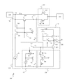
- FIG. 1 is a scheme of a measuring circuit in accordance with an embodiment.
- FIG. 2 is a functional block diagram illustrating the phases of the operation of the measuring circuit of FIG. 1 in accordance with an embodiment.
- FIG. 1 is a diagram of a measuring circuit 100 in accordance with an embodiment for measuring the leakage current flowing in a portion 105 of an electronic device (not shown) when this portion 105 is biased by a biasing unit 110 for the electronic device.
- the measuring circuit 100 and the electronic device including the portion 105 and the biasing unit 110 may, for example, be integrated in a same semiconductor chip, such as a silicon chip.
- the electronic device may be a memory device, for example, a non-volatile memory device such as a flash memory, with the portion 105 that may be the junction between an n-type well and the p-type substrate of the electronic device, or the junction between the drain active area of an n-channel MOS transistor and the p-type well in which the transistor is realized in the electronic device, and the biasing unit 110 which may be a booster circuit for the electronic device—such as for example a charge pump—adapted to reverse bias this junction.
- a memory device for example, a non-volatile memory device such as a flash memory
- the portion 105 that may be the junction between an n-type well and the p-type substrate of the electronic device, or the junction between the drain active area of an n-channel MOS transistor and the p-type well in which the transistor is realized in the electronic device
- the biasing unit 110 which may be a booster circuit for the electronic device—such as for example a charge pump—adapted to reverse bias this junction.
- the measuring circuit 100 includes five main sections 115 , 120 , 125 , 130 , 150 .
- the section 115 includes a first p-channel MOS transistor M 1 and a second p-channel MOS transistor M 2 .
- the transistor M 1 has a control node for receiving a control digital signal A (adapted to assume a high logic value and a low logic value), a first conduction node coupled to the biasing unit 110 for receiving a bias voltage Vb, and a second conduction node coupled to the portion 105 of the electronic device 105 to provide the bias voltage Vb when the control digital signal A is at the low logic value.
- the transistor M 2 has a control node adapted to receive a control digital signal An corresponding to the logical negation (the complement) of the control digital signal A, a first conduction node coupled to the biasing unit 110 through the section 120 to receive the bias voltage Vb, and a second conduction node coupled to the portion 105 of the electronic device to provide the bias voltage Vb when the control digital signal An is at the low logic value.
- the section 120 includes a p-channel MOS transistor M 3 having a first conduction node coupled to the first conduction node of the transistor M 1 (defining a circuit node N 1 ), a second conduction node coupled to the first conduction node of the transistor M 2 (defining a circuit node N 2 ), and a control node coupled to the control nodes of three additional p-channel MOS transistors M 4 , M 5 , M 6 (defining a circuit node N 3 ).
- the transistor M 4 also has a first conduction node coupled to the node N 1 and a second conduction node coupled to a first conduction node of the transistor M 5 .
- the transistor M 6 also has a first conduction node coupled to the node N 2 and a second conduction node coupled to the sections 125 , 130 and 150 (defining a circuit node N 4 ).
- the transistor M 5 is coupled in a diode configuration, with a second conduction node coupled to its control node (and thus to the node N 3 ).
- the section 120 further includes a constant current generator Is having a first node coupled to the node N 3 and a second node coupled to a reference node, here a reference node GND for receiving the ground voltage.
- the section 125 includes an n-channel MOS transistor M 7 having a first conduction node coupled to the node N 4 , a second conduction node coupled to the reference node GND, and a control node coupled to a first node of a first storage capacitor C 1 .
- the first storage capacitor C 1 has a second node coupled to the reference node GND.
- the section 125 further includes an electronic switch S 1 having a first conduction node coupled to the control node of the transistor M 7 and a second conduction node coupled to the node N 4 .
- the electronic switch S 1 is controlled by a control digital signal S (adapted to assume a high logic value and a low logic value), which determines the opening-closing state thereof.
- the electronic switch S 1 is open, and the switch's first conduction node and the second conduction node are electrically isolated from one another, while if the control digital signal S is at the high logic value, the switch S 1 closes, electrically coupling the switch's first conduction node to the switch's second conduction node.
- the section 130 includes an n-channel MOS transistor M 8 having a first conduction node coupled to the reference node GND, a second conduction node coupled to a first conduction node of an electronic switch S 2 , and a control node adapted to receive a comparison analog signal SC (which signal is adapted to assume any value between the ground voltage and the supply voltage, as will be described in detail in a following portion of this description).
- the electronic switch S 2 has a second conduction node coupled to the node N 4 .
- the electronic switch S 2 is controlled by the control digital signal S, which determines the opening-closing state thereof in the same way as for the electronic switch S 1 .
- the section 150 includes a comparator circuit including an n-channel MOS transistor M 9 , a p-channel MOS transistor M 10 , a capacitor C 2 and an electronic switch S 3 .
- the transistor M 9 has a first conduction node coupled to the reference node GND, a second conduction node coupled to a first conduction node of the transistor M 10 (defining a circuit node N 5 ), and a control node coupled to the node N 4 .
- the transistor M 10 has a second control node coupled to a power supply node Vdd to receive a supply voltage, and a control node coupled to a first node of the capacitor C 2 .
- the capacitor C 2 has a second node coupled to the supply node Vdd.
- the electronic switch S 3 has a first conduction node coupled to the control node of the transistor M 10 , and a second conduction node coupled to the node N 5 .
- the electronic switch S 3 is controlled by the control digital signal S, which determines the opening-closing state thereof in the same way as for the electronic switch S 1 and the electronic switch S 2 .
- the section 150 further includes a logic inverter INV having an input node coupled to the node N 5 and an output node for providing a detection digital signal SO.
- the operation of the measuring circuit 100 in accordance with an embodiment provides for the repetition of an operating cycle including four distinct phases F 1 , F 2 , F 3 , F 4 .
- the control digital signal A is set to the low logic level, the control digital signal An to the high logic level, and the control digital signal S to the low logic level.
- the transistor M 1 is on and the transistor M 2 is off, and the portion 105 of the electronic device is biased with the bias voltage Vb generated by the biasing unit 110 .
- the (possible) leakage current that is generated in the biasing of the portion 105 of the electronic device flows from the biasing unit 110 to this portion 105 through the transistor M 1 .
- the electronic switches S 1 , S 2 , and S 3 are all open.
- control digital signals A and An are kept to the logic levels of the first phase, while the control digital signal S is set to a high logic level.
- the current Is generated by the constant current generator Is is mirrored by the transistors M 3 -M 6 from the section 120 to the node N 4 ; consequently, because the transistors M 3 -M 6 are sized accordingly, the current Im( 2 ) flowing through the transistor M 6 is substantially equal to Is.
- the current Im( 2 ) is subdivided at the node N 4 into a current Isc( 2 ) flowing in the transistor M 8 (which in this phase is conductive, being that the electronic switch S 2 is closed) and into a current Ir( 2 ) flowing in the transistor M 7 .
- the intensity of the current Isc( 2 ) is set by transistor M 8 based on the comparison analog signal SC supplied to the control node of this transistor. Since the electronic switch S 1 is closed, the control node of the transistor M 7 turns out to be electrically coupled to the node N 4 , and the voltage Vx( 2 ) that develops on the node N 4 due to the current Ir( 2 ) which flows through the transistor M 7 is stored across the capacitor C 1 .
- a corresponding voltage Vo( 2 ) develops on the node N 5 , which is a function of the voltage Vx( 2 ) and of the ratio between the areas of the transistors M 9 and M 10 . Given that the electronic switch S 3 in this phase is closed, this voltage Vo is also stored across the capacitor C 2 .
- the voltage Vx( 2 ) therefore, depends on the comparison analog signal SC, but it does not depend on the leakage current Il, as the current Im( 2 ) is equal to the current Is generated by the constant current generator Is, and the current Isc( 2 ) is determined by the value of the comparison analog signal SC.
- the control digital signal A is set to a high logic level, the control digital signal An to a low logic level, and the control digital signal S to the low logic level.
- the transistor M 1 is off and the transistor M 2 is on.
- the leakage current Il that is generated from the biasing of the portion 105 of the electronic device flows from the biasing unit 110 to this portion 105 through the transistors M 3 and M 2 .
- the electronic switches S 1 , S 2 , and S 3 are again all open.
- the control node of the transistor M 7 is biased with a voltage value equal to the value of the voltage Vx( 2 ) of the second phase, while the control node of the transistor M 10 is biased with a voltage value equal to the value of the voltage Vo( 2 ) of the second phase.
- phase F 3 the transistor M 6 turns out to conduct a current Im( 3 ) that also depends on the leakage current Il.
- the transistors M 3 and M 6 are no longer coupled in series as in step F 2 , because the transistor M 2 sinks from the node N 2 a current equal to Il.
- the current Isc( 2 ) is used as a comparison threshold for the leakage current Il.
- the current Isc( 2 ) is set to a respective different value at each repetition of step F 2 .
- the comparator circuit of the section 150 is configured to discern if the state defined by the current Isc( 2 ) set in step F 2 and by the current Il measured in phase F 3 is the state ST 1 or the state ST 2 .
- the comparator circuit of the section 150 acts as an inverter having the node N 4 which serves as the input node, the node N 5 serving as the output node, and a switching threshold depending on the voltage Vo( 2 )—stored across the capacitor C 2 in the phase F 2 —which in turn depends on the voltage Vx( 2 ), and thus on the current Isc( 2 ).
- the transistors M 9 and M 10 are sized in such a way that:
- the circuit nodes of the circuit 100 and the capacitors C 1 , C 2 are discharged, for example through a coupling to the ground node via appropriate discharge routes that can be selectively activated (not shown in the figure).
- the measurement of leakage current Il is carried out by repeating the operating cycle including the sequence of phases F 1 , F 2 , F 3 , F 4 , setting the voltage SC the first time the phase F 2 is carried out to a value corresponding to a current Isc( 2 ) that is greater than the maximum leakage current Il that is not desired, and decreasing this voltage at each subsequent repetition of the operating cycle—specifically, for each repetition of the phase F 2 —until it is observed a switching of the detection signal SO from the high logic value (indicative of the state ST 1 ) to the low logic value (indicative of the state ST 2 ).
- the leakage current Il exceeds the threshold Isc( 2 )
- the actual value of the leakage current Il that flows from the biasing unit 110 to the portion 105 of the electronic device is between the value Isc( 2 ) corresponding to the reiteration of the phase F 2 in the operating cycle prior to the switching of the detection signal SO and the value Isc( 2 ) corresponding to the reiteration of the phase F 2 in the operating cycle in which the detection signal SO is switched.
- the voltage SC is set to a value corresponding to a current Isc( 2 ) that is null, and increasing the voltage at each subsequent repetition of the phase F 2 , until a switching of the detection signal SO is observed from the low logic value (indicative of the state ST 2 ) to the high logic value (indicative of the state ST 1 ).
- the resolution of this measurement is related to the step change in Isc( 2 ) from iteration to iteration, particularly the step change in Isc( 2 ) between the iterations before and after the switching of the level of SO; the smaller this step change, the higher the resolution, and the larger this step change, the lower the resolution.
- the circuit 100 of FIG. 1 and the device whose leakage current the circuit 100 measures may be disposed on an integrated circuit, which may be coupled to one or more other integrated circuits.
- One or more of these integrated circuits may be, or may include, a computing circuit such as a microprocessor or a microcontroller. And some or all of these integrated circuits may be disposed on a same integrated-circuit die, or some or all of these integrated circuits may be disposed on respective integrated-circuit dies.
Abstract
Description
Ir(2)=Im(2)−Isc(2)=Is−Isc(2) (1)
Im(3)=Is−Il (2)
Ir(3)=Im(3)=Is−Il (3)
ST1: Ir(3)>Ir(2)→Il<Isc(2)
ST2: Ir(3)<Ir(2)→Il>Isc(2).
ST1: Vx(3)>Vx(2)→Il<Isc(2)
ST2: Vx(3)<Vx(2)→Il>Isc(2)
-
- in the state ST1, or with Vx(3)>Vx(2), the voltage Vo(3) assumes a value sufficiently low to ensure that the logic inverter INV brings the detection digital signal SO to the high logic value, and
- in the state ST2, or with Vx(3)<Vx(2), the voltage Vo(3) assumes a value sufficiently high to ensure that the logic inverter INV brings the detection digital signal SO to the low logic value.
Claims (19)
Applications Claiming Priority (3)
| Application Number | Priority Date | Filing Date | Title |
|---|---|---|---|
| ITMI2013A1144 | 2013-07-08 | ||
| ITMI20131144 | 2013-07-08 | ||
| ITMI2013A001144 | 2013-07-08 |
Publications (2)
| Publication Number | Publication Date |
|---|---|
| US20150008939A1 US20150008939A1 (en) | 2015-01-08 |
| US9442149B2 true US9442149B2 (en) | 2016-09-13 |
Family
ID=49118651
Family Applications (1)
| Application Number | Title | Priority Date | Filing Date |
|---|---|---|---|
| US14/326,263 Active 2034-11-03 US9442149B2 (en) | 2013-07-08 | 2014-07-08 | Measuring leakage currents and measuring circuit for carrying out such measuring |
Country Status (1)
| Country | Link |
|---|---|
| US (1) | US9442149B2 (en) |
Families Citing this family (2)
| Publication number | Priority date | Publication date | Assignee | Title |
|---|---|---|---|---|
| US10289679B2 (en) * | 2014-12-10 | 2019-05-14 | International Business Machines Corporation | Data relationships in a question-answering environment |
| CN112305450A (en) * | 2019-07-26 | 2021-02-02 | 西安格易安创集成电路有限公司 | Electric leakage detection circuit |
Citations (5)
| Publication number | Priority date | Publication date | Assignee | Title |
|---|---|---|---|---|
| US5838524A (en) * | 1997-03-21 | 1998-11-17 | Cherry Semiconductor Corporation | Current limit circuit for inhibiting voltage overshoot |
| JP2000275300A (en) | 1999-03-24 | 2000-10-06 | Matsushita Electric Ind Co Ltd | Semiconductor device |
| US6201479B1 (en) | 1996-10-24 | 2001-03-13 | Continental Teves Ag & Co., Ohg | Switching arrangement for monitoring leakage current |
| US20060248416A1 (en) | 2005-04-12 | 2006-11-02 | Advantest Corporation | Test apparatus and test method |
| US20100257492A1 (en) * | 2009-04-07 | 2010-10-07 | International Business Machines Corporation | On-chip leakage current modeling and measurement circuit |
-
2014
- 2014-07-08 US US14/326,263 patent/US9442149B2/en active Active
Patent Citations (5)
| Publication number | Priority date | Publication date | Assignee | Title |
|---|---|---|---|---|
| US6201479B1 (en) | 1996-10-24 | 2001-03-13 | Continental Teves Ag & Co., Ohg | Switching arrangement for monitoring leakage current |
| US5838524A (en) * | 1997-03-21 | 1998-11-17 | Cherry Semiconductor Corporation | Current limit circuit for inhibiting voltage overshoot |
| JP2000275300A (en) | 1999-03-24 | 2000-10-06 | Matsushita Electric Ind Co Ltd | Semiconductor device |
| US20060248416A1 (en) | 2005-04-12 | 2006-11-02 | Advantest Corporation | Test apparatus and test method |
| US20100257492A1 (en) * | 2009-04-07 | 2010-10-07 | International Business Machines Corporation | On-chip leakage current modeling and measurement circuit |
Non-Patent Citations (1)
| Title |
|---|
| Search Report for Italian patent application No. MI20131144; Munich, Germany, Mar. 19, 2014; 2 pages. |
Also Published As
| Publication number | Publication date |
|---|---|
| US20150008939A1 (en) | 2015-01-08 |
Similar Documents
| Publication | Publication Date | Title |
|---|---|---|
| Luo et al. | A sub-10 mV power converter with fully integrated self-start, MPPT, and ZCS control for thermoelectric energy harvesting | |
| US7084695B2 (en) | Method and apparatus for low voltage temperature sensing | |
| KR101766971B1 (en) | Combination current generator configured to selectively generate one of a ptat and a ctat current | |
| US6937074B2 (en) | Power-up signal generator in semiconductor device | |
| US20060140018A1 (en) | Semiconductor memory device | |
| TWI446355B (en) | Sensing circuit for memory cell with low supply power | |
| US6750696B2 (en) | Level conversion circuit converting logic level of signal | |
| US7135913B2 (en) | Reference voltage generating circuit for integrated circuit | |
| KR100712545B1 (en) | Sectional temperature sensor and sectional temperature detecting method | |
| US7482847B2 (en) | Power-on reset circuit | |
| KR100618876B1 (en) | Sequential tracking temperature sensor and temperature detecting method having hysteresis characteristic | |
| US9442149B2 (en) | Measuring leakage currents and measuring circuit for carrying out such measuring | |
| US20060038625A1 (en) | Oscillator circuit for EEPROM high voltage generator | |
| US7576575B2 (en) | Reset signal generator in semiconductor device | |
| TWI668931B (en) | Temperature determination circuit and power management circuit | |
| JP2012251917A (en) | Temperature detection circuit | |
| US9960770B2 (en) | Semiconductor integrated circuit device regarding the detection of degradation | |
| US8767498B2 (en) | Circuit and method for generating a read signal | |
| KR101222110B1 (en) | Semiconductor device | |
| US9160334B2 (en) | Semiconductor device | |
| KR100554840B1 (en) | Circuit for generating a power up signal | |
| US11581888B1 (en) | Power-on reset circuit with reduced detection time | |
| JP7236866B2 (en) | LIN receiver | |
| KR100833416B1 (en) | Power up reset circuit | |
| KR100232894B1 (en) | Auto mode selector for semiconductor memory |
Legal Events
| Date | Code | Title | Description |
|---|---|---|---|
| AS | Assignment |
Owner name: STMICROELECTRONICS S.R.L., ITALY Free format text: ASSIGNMENT OF ASSIGNORS INTEREST;ASSIGNORS:PASOTTI, MARCO;DE SANTIS, FABIO;SIGNING DATES FROM 20140710 TO 20140716;REEL/FRAME:033782/0516 |
|
| STCF | Information on status: patent grant |
Free format text: PATENTED CASE |
|
| MAFP | Maintenance fee payment |
Free format text: PAYMENT OF MAINTENANCE FEE, 4TH YEAR, LARGE ENTITY (ORIGINAL EVENT CODE: M1551); ENTITY STATUS OF PATENT OWNER: LARGE ENTITY Year of fee payment: 4 |
|
| AS | Assignment |
Owner name: STMICROELECTRONICS INTERNATIONAL N.V., SWITZERLAND Free format text: ASSIGNMENT OF ASSIGNORS INTEREST;ASSIGNOR:STMICROELECTRONICS S.R.L.;REEL/FRAME:061828/0243 Effective date: 20221025 |
|
| MAFP | Maintenance fee payment |
Free format text: PAYMENT OF MAINTENANCE FEE, 8TH YEAR, LARGE ENTITY (ORIGINAL EVENT CODE: M1552); ENTITY STATUS OF PATENT OWNER: LARGE ENTITY Year of fee payment: 8 |