US7642864B2 - Circuits and design structures for monitoring NBTI (negative bias temperature instability) effect and/or PBTI (positive bias temperature instability) effect - Google Patents
Circuits and design structures for monitoring NBTI (negative bias temperature instability) effect and/or PBTI (positive bias temperature instability) effect Download PDFInfo
- Publication number
- US7642864B2 US7642864B2 US12/021,459 US2145908A US7642864B2 US 7642864 B2 US7642864 B2 US 7642864B2 US 2145908 A US2145908 A US 2145908A US 7642864 B2 US7642864 B2 US 7642864B2
- Authority
- US
- United States
- Prior art keywords
- terminal
- drain
- coupled
- stress
- voltage
- Prior art date
- Legal status (The legal status is an assumption and is not a legal conclusion. Google has not performed a legal analysis and makes no representation as to the accuracy of the status listed.)
- Active, expires
Links
Images


Classifications
-
- H—ELECTRICITY
- H03—ELECTRONIC CIRCUITRY
- H03K—PULSE TECHNIQUE
- H03K3/00—Circuits for generating electric pulses; Monostable, bistable or multistable circuits
- H03K3/02—Generators characterised by the type of circuit or by the means used for producing pulses
- H03K3/027—Generators characterised by the type of circuit or by the means used for producing pulses by the use of logic circuits, with internal or external positive feedback
- H03K3/03—Astable circuits
- H03K3/0315—Ring oscillators
Definitions
- the present invention generally relates to electronic circuitry, with associated design structures, and, more particularly, to electronic circuits for assessing bias temperature instability effects, with associated design structures.
- CMOS complementary metal oxide semiconductor
- NBTI Negative Bias Temperature Instability
- PBTI Positive Bias Temperature Instability
- NBTI test-circuits employ a simple ring oscillator circuit 100 , as shown in FIG. 1 .
- the frequency of ring oscillator 100 is measured before stress. In stress mode, the ring is disabled from oscillation and the supply voltage and/or temperature are increased to facilitate an accelerated stressing of the devices. Since PBTI has been considered insignificant, the impact of stress on the NFETs 102 has been ignored. After suitably stressing the ring-oscillator circuit 100 , its frequency is measured again, and the difference in the pre- and post-stress frequencies is a direct indication of the extent of NBTI related degradation of the PFET devices 104 in the circuit. Note that circles 106 indicate PMOS devices under stress while circle 108 indicates and NMOS device under stress. Note also that the connection between output 110 and input 112 is omitted for clarity, and that transistors are referred to herein generically as devices.
- U.S. Pat. No. 6,476,632 to La Rosa, et al. discloses a ring oscillator design for metal oxide semiconductor field effect transistor (MOSFET) device reliability investigations and its use for in-line monitoring.
- MOSFET metal oxide semiconductor field effect transistor
- RO Ring Oscillator
- the method includes the steps of: a) selecting one inverter from the inverter stages of the RO, the selected inverter having testable nodes, the testable nodes being connected to inputs and outputs of the NMOS and a PMOS field-effect transistor (FET) forming the selected inverter; b) simultaneously stressing under a set of stress conditions 1) all of the NMOS FETs of each of the inverter stages, 2) all of the PMOS FETs, and 3) all of the NMOS FETs and PMOS FETs in the RO; c) measuring a shift in selected device parameters in the selected inverter; d) measuring a frequency degradation of the entire RO; and e) establishing a relationship between the shift in the device parameters and the frequency degradation and relating the relationship to a known degradation mechanism.
- FET PMOS field-effect transistor
- on-chip pass gates controlled by appropriate off-chip DC voltage signals allow parallel DC stressing, as well as forcing an off-chip AC voltage waveform to a given MOSFET type device (either PMOSFET or NMOSFET) on every inverter stage of the RO.
- MOSFET type device either PMOSFET or NMOSFET
- the RO circuit makes it possible to investigate the effect on the RO frequency degradation, caused by any DC MOSFET degradation mechanism as well as by any external AC voltage waveform known to be representative of a critical circuit operation.
- the dependence of the RO frequency on device degradation mechanisms activated during a critical circuit operation can be carefully investigated and quantified.
- Principles of the present invention provide techniques for monitoring NBTI and PBTI effects individually, and in combination.
- a NOR-gate based ring oscillator circuit for measurement of negative bias temperature instability effect includes a ring oscillator with an odd number of NOR-gates greater than or equal to three.
- Each of the NOR-gates has first and second input terminals, a voltage supply terminal, and an output terminal. The first input terminals of all the NOR-gates are interconnected, and each of the NOR-gates has its output terminal connected to the second input terminal of an immediately adjacent one of the NOR-gates.
- a voltage supply and control block also included. During a stress mode, this block applies a stress enable signal to the interconnected first input terminals, and an increased supply voltage to the voltage supply terminals. During a measurement mode, this block applies ground voltage to the interconnected first input terminals, and a normal supply voltage to the voltage supply terminals.
- a NAND-gate based ring oscillator circuit for measurement of positive bias temperature instability effect includes a ring oscillator with an odd number of NAND-gates greater than or equal to three.
- Each of the NAND-gates has first and second input terminals, a voltage supply terminal, and an output terminal. The first input terminals of all the NAND-gates are interconnected.
- Each of the NAND-gates has its output terminal connected to the second input terminal of an immediately adjacent one of the NAND-gates.
- a voltage supply and control block is also included. During a stress mode, this block applies a stress enable signal to the interconnected first input terminals, and an increased supply voltage to the voltage supply terminals. During a measurement mode, this block applies normal supply voltage to the interconnected first input terminals, and a normal supply voltage to the voltage supply terminals.
- a ring oscillator circuit for measurement of negative bias temperature instability effect and positive bias temperature instability effect includes a ring oscillator with first and second rails and an odd number of repeating circuit structures greater than or equal to three.
- Each of the repeating circuit structures includes an input terminal and an output terminal, a first p-type transistor, a first n-type transistor, and repeating-circuit-structure control circuitry.
- the first p-type transistor has a gate coupled to the input terminal, a first drain-source terminal coupled to the first rail, and a second drain source terminal selectively coupled to the output terminal.
- the first n-type transistor has a gate coupled to the input terminal, a first drain-source terminal coupled to the second rail, and a second drain source terminal selectively coupled to the output terminal.
- Each of the repeating circuit structures has its output terminal connected to the input terminal of an immediately adjacent one of the repeating circuit structures.
- a voltage supply and control block coupled to the ring oscillator and configured to cooperate with the repeating-circuit-structure control circuitry, as follows. During a negative bias temperature instability effect direct current test mode, a stress voltage is applied to the first rail and a ground to the second rail, and the first p-type transistor of each of the repeating circuit structures is stressed.
- a stress voltage is applied to the first rail and a ground to the second rail and the first n-type transistor of each of the repeating circuit structures is stressed.
- a nominal supply voltage is applied to the first rail and a ground to the second rail, and the second drain source terminals of the first n-type transistors and the first p-type transistors are coupled to the output terminals, such that each of the repeating circuit structures functions as an inverter.
- a ring oscillator circuit for measurement of negative bias temperature instability effect and positive bias temperature instability effect includes a ring oscillator.
- the ring oscillator includes an odd number of main inverters greater than or equal to three.
- Each of the main inverters has an input terminal, an output terminal, a voltage supply terminal, a p-type transistor, and an n-type transistor.
- a plurality of first paths selectively couple the output terminals of the main inverters to the input terminals of adjacent ones of the main inverters.
- a plurality of inverting second paths selectively couple the output terminals of the main inverters to the input terminals of adjacent ones of the main inverters.
- a voltage supply and control block coupled to the ring oscillator and configured to effectuate the following.
- a negative bias temperature instability effect test mode the input of a first one of the inverters is grounded, a stress voltage is applied to the voltage supply terminals of the main inverters, the first paths are opened, and the second paths are operative to invert a signal appearing at the output terminals of the main inverters to obtain an inverted signal, and to supply the inverted signal to the input terminals of the adjacent ones of the main inverters, thus stressing the p-type transistors.
- the stress voltage is applied to the voltage supply terminals of the main inverters and the input of the first one of the inverters, the first paths are opened, and the second paths are operative to invert a signal appearing at the output terminals of the main inverters to obtain an inverted signal, and to supply the inverted signal to the input terminals of the adjacent ones of the main inverters, thus stressing the n-type transistors.
- a nominal voltage is applied to the voltage supply terminals of the main inverters, the first paths are conductive and the second paths are opened.
- a circuit for measuring bias temperature instability effect in pass gates includes a ring oscillator.
- the oscillator has an odd number of inverters greater than or equal to three.
- Each of the inverters has an input terminal, an output terminal, and first and second voltage supply terminals. The first voltage supply terminals of all the inverters are coupled, and the second voltage supply terminals of all the inverters are coupled.
- a plurality of pass transistors are configured as the pass gates, coupling the output terminals of the inverters to the input terminals of adjacent ones of the inverters.
- a plurality of supplemental transistors selectively couple the inputs of the inverters to (i) the second voltage supply terminals, in a case when the pass transistors are p-type, and (ii) the first voltage supply terminals, in a case when the pass transistors are n-type.
- a voltage supply and control block is coupled to the ring oscillator and configured such that in a stress mode, the pass transistors are stressed and the supplemental transistors are on; and in a measurement mode, the pass transistors operate with nominal voltage and the supplemental transistors are off.
- the invention includes design structures for circuits of the kind described.
- One or more embodiments of the present invention may be realized in the form of an integrated circuit.
- FIG. 1 shows a ring oscillator, as known from the prior art
- FIG. 2 shows a NOR-gate based ring oscillator for NBTI measurement, according to an aspect of the invention
- FIG. 3 shows a NAND-gate based ring oscillator for PBTI measurement, according to another aspect of the invention
- FIG. 4 depicts an embodiment of an inventive repeating unit that can be used for both NBTI and PBTI measurement
- FIG. 5 shows the unit of FIG. 4 under NBTI DC stress
- FIG. 6 shows the unit of FIG. 4 under PBTI DC stress
- FIG. 7 shows the unit of FIG. 4 in measurement mode
- FIG. 8 shows the unit of FIG. 4 in NBTI source pulsing mode
- FIG. 9 depicts an exemplary embodiment of an isolated NBTI/PBTI measurement circuit, according to another aspect of the invention, in NBTI stress mode
- FIG. 10 depicts the circuit of FIG. 9 in PBTI stress mode
- FIG. 11 depicts the circuit of FIG. 9 in measurement mode
- FIG. 12 depicts an exemplary embodiment of circuit for NBTI measurement in PMOS pass gates, according to yet another aspect of the invention, in NBTI stress mode
- FIG. 13 depicts the circuit of FIG. 12 in NBTI measurement mode
- FIG. 14 depicts an exemplary embodiment of circuit for PBTI measurement in NMOS pass gates, according to still another aspect of the invention, in PBTI stress mode;
- FIG. 15 depicts the circuit of FIG. 14 in PBTI measurement mode
- FIGS. 16-18 depict non-limiting exemplary applications of one or more embodiments of the invention.
- FIG. 19 is a flow diagram of a design process used in semiconductor design, manufacture, and/or test.
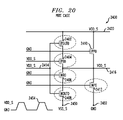
- FIG. 20 shows the unit of FIG. 4 in PBTI source pulsing mode.
- One or more embodiments of the invention provide test structures and schemes that enable efficient characterization and analysis of both PBTI and NBTI effects, and their impact on circuits. Since the dependencies, mechanisms and magnitudes of PBTI and NBTI may differ, it is advantageous to be able to isolate the impact of each of these two effects.
- the simplicity of the ring-oscillator based configuration is maintained, while the two types of devices (n and p) are isolated using simple switches and pre-bias circuits.
- these switches are closed and pre-bias circuits are disabled, so that the circuit operates as a ring-oscillator.
- In stress mode these switches are open; thereby eliminating the interaction between the two types of stressed devices, while the requisite stress voltages are applied via the pre-bias circuits.
- One or more embodiments of the invention isolate the contributions of the two effects; this isolation is believed to be advantageous since, in the prior-art ring oscillator approach, the difference in frequency is in fact influenced by the degradation of PFETs due to NBTI and of NFETs due to PBTI, during the stress.
- NOR-gate based ring oscillator system 200 wherein the devices DUT (device under test), PB and ND impact the ring-oscillator delay, as depicted in FIG. 2 .
- FIG. 2 depicts three NOR gates numbered 0 , 1 , 2 , any odd number greater than or equal to three can be employed. Accordingly, reference is made to an “Nth” device in the following discussion. Note also that feedback from the last gate's output to the first gate's input is not shown, for illustrative convenience (true throughout the specification).
- the Stress_En signal is asserted and the supply voltage V CC — rsc is increased. This turns off the second device in the PMOS stack (i.e. PB 0 thru PB N ), numbered 202 , 204 , 206 , and ensures that the parallel NFET devices (i.e. NS 0 thru NS N ), numbered 208 , 210 , 212 , are turned on.
- the devices NS 0 thru NS N 208 , 210 , 212 also experience stress in this scenario, they are turned off during measurement mode and do not impact the frequency of the ring-oscillator system 200 .
- the difference between pre- and post-stress frequency is only a function of the NBTI effect on the PFET devices PB 0 thru PB N , 202 , 204 , 206 , and is independent of PBTI effects.
- the Stress_En signal is de-asserted (that is, block 250 applies a zero or ground voltage to the terminal labeled STRESS_EN), and the circuit 200 operates as a simple ring-oscillator.
- a normal supply voltage is applied to the voltage supply terminals (i.e., upper rail) in this mode.
- the devices PB 0 to PB N , 202 , 204 , 206 are sized larger than the DUTs 220 , 222 , 224 , to increase and preferably maximize the NBTI effect on the delay and thus improve the sensitivity of the ring-oscillator 200 to NBTI-induced degradation.
- the sensitivity of the system is better than the conventional ring oscillator based scheme, since all the PFET devices experience stress during the stress mode, as opposed to the conventional ring oscillator based scheme, where only alternate PFET devices experience stress, as shown in FIG. 1 .
- FIG. 2 Also shown in FIG. 2 is voltage supply/control block 250 with a plurality of terminals 252 .
- Block 250 is coupled to the circuit 200 , as suggested by the ellipses, and applies the correct voltages to each terminal for stress, measurement, and so on.
- Each circuit depicted herein can be provided with a similar voltage supply/control block, but such block is omitted from the remainder of the figures for brevity and illustrative convenience.
- a complementary NAND-gate based ring-oscillator system 300 can be used for PBTI measurement, as illustrated in FIG. 3 .
- a two-high NFET stack is used, with the top device in the stack, NB 0 through NB N , numbered 302 , 304 , 306 , turned off in stress mode thereby isolating the DUTs DUT 0 through DUT N , numbered 308 , 310 , 312 .
- the parallel PFET devices PS 0 thru PS N ensure that the gate-output nodes (N 0 thru N N ), numbered 320 , 322 , 324 are at a logical high, thereby stressing the DUTs 308 , 310 , 312 (for clarity, note that with regard to the gate output nodes (N 0 thru N N ), N 1 is the output of gate 0 , N 2 is the output of gate 1 , and N 0 is the output of gate 2 ).
- a block such as block 250 applies the stress enable signal as shown (0 V, or ground, in this case), and an increased supply voltage to the top rail.
- this block applies normal supply voltage to the STRESS_EN terminal, and a normal supply voltage to the top rail.
- the top rail (supply voltage rail) voltage is increased to the higher stress voltage and the lower rail (VSS_rsc in FIG. 3 ) voltage remains at ground.
- the STRESS_EN voltage In stress mode, the STRESS_EN voltage is 0V (or ground). In measurement mode, the top rail voltage is reduced to normal supply voltage and VSS_rsc remains at 0V (or ground). The STRESS_EN voltage is normal supply voltage in the measurement node.
- the NBs There are sizing considerations analogous to FIG. 2 , that is, the NBs should be sized larger than the DUTs to increase sensitivity to the positive bias temperature instability effect.
- the PBTI and NBTI measurement systems of FIGS. 2 and 3 can be combined, as shown in FIG. 4 , into a single ring-oscillator system 400 , using a two-high stack for both PFET and NFET devices, with parallel PFET and NFET devices 410 , 412 that ensure the application of appropriate stress voltages to the DUTs in stress mode, as shown in FIGS. 5 and 6 .
- Measurement mode is shown in FIG. 7 .
- the repeating circuit structure 400 includes stacked PMOS device under test 402 and PMOS PB 404 , as well as stacked NMOS NB 406 and NMOS device under test 408 .
- N 0 414 is the input and N 1 416 is the output.
- the top and bottom rails are numbered, respectively, 418 , 420 .
- the extra devices used to provide isolation functionality are referred to as repeating-circuit-structure control circuitry, for example, devices 404 , 406 , 410 , 412 .
- the gates of all devices 404 may be interconnected to a p-stress enable terminal
- the gates of all devices 406 may be interconnected to an n-stress enable terminal
- the gates of all devices 410 may be connected to a p-parallel terminal
- the gates of all devices 412 may be connected to an n-parallel terminal.
- NBTI DC stress mode as in FIG. 5 , input 414 is grounded, and V DD — S , the elevated stress voltage, is applied to the top rail 418 and the gates of devices 404 , 410 , 412 .
- Bottom rail 420 is also grounded, as is the gate of device 406 . This results in a ground appearing also on output 416 , with devices 404 , 406 , 408 , 410 off and device 402 stressed.
- the ground at 416 will also result in stressing the next PMOS device 402 in the next repeating structure 400 .
- V DD — S is applied to top rail 418 as well as input 414 and the gate of device 404 , with bottom rail 420 and the gates of devices 406 , 410 and 412 grounded. This results in V DD — S appearing at output 416 , so that the next NMOS device 408 in the next repeating structure 400 will also be stressed. Device 408 is stressed while devices 402 , 404 , 406 and 412 are off.
- V DD is applied to top rail 418 , as well as the gates of devices 406 , 410 , while bottom rail 420 and the gates of devices 404 , 412 are grounded, reducing the structure to an inverter, where signal A applied at input 414 has its complement appear at output 416 .
- AC stress can be applied to either the PMOS or the NMOS in an inverter stage by applying the stress to the source node of the PMOS only (for the NBTI case) or the source node of the NMOS only (for the PBTI case).
- FIG. 8 AC stress can be applied to either the PMOS or the NMOS in an inverter stage by applying the stress to the source node of the PMOS only (for the NBTI case) or the source node of the NMOS only (for the PBTI case).
- FIG. 8 depicts the NBTI case, wherein input 414 , bottom rail 420 , and the gate of device 406 are grounded, while terminal 452 and the gates of devices 404 , 410 , 412 are maintained at V DD — S . Ground also appears at the output 416 .
- Waveform 454 is applied at terminal 450 , subjecting device 402 to AC stress.
- Devices 404 , 406 , 408 , 410 are off.
- the rail 418 can be formed from a test rail for applying signal 454 to 450 and a parallel rail for applying V DD — S to 452 .
- the PBTI case 2400 is shown in FIG. 20 , during alternating current stress mode.
- the source node 2450 of NDUT 0 2408 and the source node 2452 of NP 0 2412 should be separated, just as the source node 450 of PDUT 0 402 and the source node 452 of PP 0 410 were separated for the NBTI case in FIG. 8 .
- an alternating voltage 2454 is applied to 2450
- DC stress voltage V DD — S is applied to the gate of 2404 and rail 2420
- the gates of devices 2406 , 2410 , and 2412 are grounded, such that device 2408 is subject to alternating current stress.
- Devices 2402 , 2404 , 2406 , and 2412 are off.
- the input is designated as 2414 and the output 2416 (elements in FIG. 20 are given the analogous number from FIG. 8 , incremented by two thousand).
- the rail 420 can be formed from a test rail for applying signal 2454 to 2450 and a parallel rail for grounding 2452 .
- FIG. 9 Another exemplary embodiment of an isolated NBTI/PBTI measurement circuit 900 , according to another aspect of the invention, is shown in FIG. 9 .
- main inverters 902 are connected by upper pass gate structures 904 , with a parallel lower path through lower inverters 908 and lower pass gate structures 906 .
- the additional path bottom pass-gates path 906 , 908
- the pass-gates 904 in the normal signal path have no stress during stress mode.
- FIG. 9 shows the NBTI stress mode.
- the top pass gates 904 are off and a zero logic level is applied to the input of the first main inverter 902 .
- the output is fed to the first lower inverter 908 , and passes through the first lower pass gate 906 , which conducts.
- the second main inverter thus also has a logical zero input, and so on for each main inverter 902 in the chain.
- the PMOS devices in each main inverter 902 are thus stressed.
- FIG. 10 shows the PBTI stress mode for the circuit of FIG. 9 .
- the top pass gates 904 are off and a stress voltage V —str is applied to the input of the first main inverter 902 .
- the output is fed to the first lower inverter 908 , and passes through the first lower pass gate 906 , which conducts.
- the second main inverter thus also has a stress voltage V —str input, and so on for each main inverter 902 in the chain.
- the NMOS devices in each main inverter 902 are thus stressed.
- the bottom path is cut off by opening lower pass gates 906 and a normal inverter chain is formed as shown in FIG. 11 . Because the measurement is executed within a few micro seconds, the degradation of the pass-gate during measurement can be ignored.
- FIG. 12 shows an exemplary embodiment of circuit 1200 for stressing PMOS pass gates to ascertain the NBTI effect, according to an even further aspect of the invention.
- supply voltage node 1202 is connected to GND and ground node 1204 is connected to V_str.
- the inverters 1206 operate like buffers with voltage drop. This voltage drop is compensated for by the PMOS connection 1208 from the internal node to ground node 1204 .
- These devices 1208 have no impact during measurement because they are turned off, as discussed below with regard to FIG. 13 .
- the current paths formed by these PMOS devices 1208 also tend to reduce or eliminate gate leakage.
- the PMOS devices 1208 whose gates are connected to supply rail 1202 , are turned on, keeping the drain and source voltage of the PMOS pass gates 1210 equal to V —str . Even if there is gate leakage current, the current path formed by the PMOS devices 1208 when they are turned on is much stronger than gate leakage, which keeps the drain and source voltage of the PMOS pass gates 1210 equal to V —str . Hence, stress voltage can be accurately controlled.
- FIG. 13 shows the circuit 1200 during measurement.
- devices 1208 By connecting the supply voltage node 1202 back to VDD and the ground node 1204 to GND, devices 1208 are off, gates 1210 still conduct, and inverters 1206 form a ring-oscillator.
- FIGS. 14 and 15 are analogous to FIGS. 12 and 13 , but for measurement of the PBTI effect in NMOS pass-gates.
- supply voltage node 1402 of circuit 1400 is connected to GND and ground node 1404 is connected to V —str .
- the inverters 1406 operate like buffers with voltage drop. This voltage drop is compensated for by the NMOS connection 1408 from the internal node to the voltage supply node 1402 .
- These devices 1408 have no impact during measurement because they are turned off, as discussed below with regard to FIG. 15 .
- the current paths formed by these NMOS devices 1408 also tend to reduce or eliminate gate leakage.
- the NMOS devices 1408 During stress mode, the NMOS devices 1408 , whose gates are connected to ground rail 1404 , are turned on, keeping the drain and source voltage of the NMOS pass gates 1410 equal to ground. (Even if there is gate leakage current, the current path formed by the NMOS devices 1408 when they are turned on is much stronger than gate leakage, which keeps the drain and source voltage of the NMOS pass gates 1410 equal to ground.) Hence, stress voltage can be accurately controlled.
- FIG. 15 shows the circuit 1400 during measurement.
- devices 1408 By connecting the supply voltage node 1402 back to VDD and the ground node 1404 to GND, devices 1408 are off, gates 1410 still conduct, and inverters 1406 form a ring-oscillator.
- FIGS. 2-15 and 20 can be used to replace prior-art simple ring oscillator configurations, or other read-out circuit configurations, as shown in FIGS. 16-18 , without need for any change to the read-out circuitry.
- an inventive embodiment labeled “X” or 1600, is substituted for another circuit such as a conventional ring oscillator circuit.
- inventive circuit 1600 is substituted for a ring oscillator critical path replica in the approach of V. Reddy et al, “Impact of Negative Bias Temperature Instability on Digital Circuit Reliability,” as presented at IRPS 2002 .
- inventive circuit 1600 is substituted for stressed and unstressed ring oscillator critical path replicas in a counter based measurement approach.
- inventive circuit 1600 is substituted for stressed and unstressed ring oscillator critical path replicas in phase comparator based measurement, as per T. Kim et al., “Silicon Odometer: An On-Chip Reliability Monitor for Measuring Frequency Degradation of Digital Circuits,” presented at the 2007 VLSI symposium.
- One exemplary advantage of one or more embodiments of the invention is the ability to measure the impact of PBTI- and NBTI-based degradation independently, while maintaining the simplicity of the ring-oscillator based system and its associated read-out circuitry.
- One or more embodiments also easily lend themselves to both AC and DC stress modes, and an analysis of stress frequency, duration, temperature and voltage on the degradation of each type of device.
- the DUT can be replaced by more complex structures if required to understand the impact of these degradations on stacked-circuit configurations.
- Circuits according to one more aspects of the present invention may be realized as integrated circuits; thus, at least a portion of the techniques of one or more aspects or embodiments of the present invention described herein may be implemented in an integrated circuit.
- a plurality of identical die are typically fabricated in a repeated pattern on a surface of a semiconductor wafer.
- Each die can include one or more of the circuits described herein, and may include other structures or circuits, or circuits having other types of cells.
- the individual die are cut or diced from the wafer, then packaged as an integrated circuit.
- a person of skill in the art will know how to dice wafers and package die to produce integrated circuits. Integrated circuits so manufactured are considered part of the present invention.
- Circuits as described above can be part of the design for an integrated circuit chip.
- the chip design can be created, for example, in a graphical computer programming language, and stored in a computer storage medium (such as a disk, tape, physical hard drive, or virtual hard drive such as in a storage access network). If the designer does not fabricate chips or the photolithographic masks used to fabricate chips, the designer may transmit the resulting design by physical means (e.g., by providing a copy of the storage medium storing the design) or electronically (e.g., through the Internet) to such entities, directly or indirectly.
- the stored design can then be converted into an appropriate format such as, for example, Graphic Design System II (GDSII), for the fabrication of photolithographic masks, which typically include multiple copies of the chip design in question that are to be formed on a wafer.
- GDSII Graphic Design System II
- the photolithographic masks can be utilized to define areas of the wafer (and/or the layers thereon) to be etched or otherwise processed.
- Resulting integrated circuit chips can be distributed by the fabricator in raw wafer form (that is, as a single wafer that has multiple unpackaged chips), as a bare die or in a packaged form.
- the chip can be mounted in a single chip package (such as a plastic carrier, with leads that are affixed to a mother board or other higher level carrier) or in a multi-chip package (such as a ceramic carrier that has either or both surface interconnections or buried interconnections).
- the chip may then be integrated with other chips, discrete circuit elements and/or other signal processing devices as part of either (a) an intermediate product, such as a mother board, or (b) an end product.
- the end product can be any product that includes integrated circuit chips, ranging from toys and other low-end applications to advanced computer products having a display, a keyboard or other input device, and a central processor.
- FIG. 19 shows a block diagram of an exemplary design flow 1900 used for example, in semiconductor design, manufacturing, and/or test.
- Design flow 1900 may vary depending on the type of IC being designed.
- a design flow 1900 for building an application specific IC (ASIC) may differ from a design flow 1900 for designing a standard component.
- Design structure 1920 is preferably an input to a design process 1910 and may come from an IP provider, a core developer, or other design company or may be generated by the operator of the design flow, or from other sources.
- Design structure 1920 comprises, for example, an embodiment of the invention as shown in FIGS. 2-18 in the form of schematics or HDL, a hardware-description language (e.g., Verilog, VHDL, C, etc.).
- Design structure 1920 may be contained on one or more machine readable media.
- design structure 1920 may be a text file or a graphical representation of an embodiment of the invention as shown in FIGS. 2-18 .
- Design process 1910 preferably synthesizes (or translates) an embodiment of the invention as shown in FIGS. 2-18 into a netlist 1980 , where netlist 1980 is, for example, a list of wires, transistors, logic gates, control circuits, I/O, models, etc. that describes the connections to other elements and circuits in an integrated circuit design and recorded on at least one machine readable medium. This may be an iterative process in which netlist 1980 is re-synthesized one or more times depending on design specifications and parameters for the circuit.
- Design process 1910 may include using a variety of inputs; for example, inputs from library elements 1930 which may house a set of commonly used elements, circuits, and devices, including models, layouts, and symbolic representations, for a given manufacturing technology (e.g., different technology nodes, 32 nm, 45 nm, 90 nm, etc.), design specifications 1940 , characterization data 1950 , verification data 1960 , design rules 1970 , and test data files 1985 (which may include test patterns and other testing information). Design process 1910 may further include, for example, standard circuit design processes such as timing analysis, verification, design rule checking, place and route operations, etc.
- One of ordinary skill in the art of integrated circuit design can appreciate the extent of possible electronic design automation tools and applications used in design process 1910 without deviating from the scope and spirit of the invention.
- the design structure of the invention is not limited to any specific design flow.
- Design process 1910 preferably translates an embodiment of the invention as shown in FIGS. 2-18 , along with any additional integrated circuit design or data (if applicable), into a second design structure 1990 .
- Design structure 1990 resides on a storage medium in a data format used for the exchange of layout data of integrated circuits and/or symbolic data format (e.g. information stored in a GDSII (GDS2), GLI, OASIS, map files, or any other suitable format for storing such design structures).
- Design structure 1990 may comprise information such as, for example, symbolic data, map files, test data files, design content files, manufacturing data, layout parameters, wires, levels of metal, vias, shapes, data for routing through the manufacturing line, and any other data required by a semiconductor manufacturer to produce an embodiment of the invention as shown in FIGS. 2-18 .
- Design structure 1990 may then proceed to a stage 1995 where, for example, design structure 1990 : proceeds to tape-out, is released to manufacturing, is released to a mask house, is sent to another design house, is sent back to the
Abstract
Description
Claims (20)
Priority Applications (1)
| Application Number | Priority Date | Filing Date | Title |
|---|---|---|---|
| US12/021,459 US7642864B2 (en) | 2008-01-29 | 2008-01-29 | Circuits and design structures for monitoring NBTI (negative bias temperature instability) effect and/or PBTI (positive bias temperature instability) effect |
Applications Claiming Priority (1)
| Application Number | Priority Date | Filing Date | Title |
|---|---|---|---|
| US12/021,459 US7642864B2 (en) | 2008-01-29 | 2008-01-29 | Circuits and design structures for monitoring NBTI (negative bias temperature instability) effect and/or PBTI (positive bias temperature instability) effect |
Publications (2)
| Publication Number | Publication Date |
|---|---|
| US20090189703A1 US20090189703A1 (en) | 2009-07-30 |
| US7642864B2 true US7642864B2 (en) | 2010-01-05 |
Family
ID=40898630
Family Applications (1)
| Application Number | Title | Priority Date | Filing Date |
|---|---|---|---|
| US12/021,459 Active 2028-03-12 US7642864B2 (en) | 2008-01-29 | 2008-01-29 | Circuits and design structures for monitoring NBTI (negative bias temperature instability) effect and/or PBTI (positive bias temperature instability) effect |
Country Status (1)
| Country | Link |
|---|---|
| US (1) | US7642864B2 (en) |
Cited By (21)
| Publication number | Priority date | Publication date | Assignee | Title |
|---|---|---|---|---|
| US20110090015A1 (en) * | 2008-09-30 | 2011-04-21 | Panasonic Corporation | Semiconductor integrated circuit and electronic device |
| US20110215827A1 (en) * | 2010-03-03 | 2011-09-08 | Qualcomm Incorporated | Method and Apparatus for Testing a Memory Device |
| US20120182079A1 (en) * | 2011-01-19 | 2012-07-19 | International Business Machines Corporation | Monitoring negative bias temperature instability (nbti) and/or positive bias temperature instability (pbti) |
| US8587383B2 (en) | 2011-12-07 | 2013-11-19 | International Business Machines Corporation | Measuring bias temperature instability induced ring oscillator frequency degradation |
| CN103513173A (en) * | 2012-06-29 | 2014-01-15 | 复旦大学 | BTI testing device based on voltage-controlled oscillator and testing method thereof |
| US8829922B2 (en) | 2011-02-17 | 2014-09-09 | International Business Machines Corporation | On-chip measurement of AC variability in individual transistor devices |
| US8952705B2 (en) | 2011-11-01 | 2015-02-10 | Nvidia Corporation | System and method for examining asymetric operations |
| US20150091601A1 (en) * | 2013-09-30 | 2015-04-02 | International Business Machines Corporation | On chip bias temperature instability characterization of a semiconductor device |
| US9086865B2 (en) | 2012-07-09 | 2015-07-21 | International Business Machines Corporation | Power napping technique for accelerated negative bias temperature instability (NBTI) and/or positive bias temperature instability (PBTI) recovery |
| US9384858B2 (en) | 2014-11-21 | 2016-07-05 | Wisconsin Alumni Research Foundation | Computer system predicting memory failure |
| US9425772B2 (en) | 2011-07-27 | 2016-08-23 | Nvidia Corporation | Coupling resistance and capacitance analysis systems and methods |
| US9448125B2 (en) | 2011-11-01 | 2016-09-20 | Nvidia Corporation | Determining on-chip voltage and temperature |
| US20160284399A1 (en) * | 2015-03-27 | 2016-09-29 | Intel Corporation | Apparatus and method for drift cancellation in a memory |
| US9496853B2 (en) | 2011-07-22 | 2016-11-15 | Nvidia Corporation | Via resistance analysis systems and methods |
| US9805787B2 (en) | 2015-11-26 | 2017-10-31 | Samsung Electronics Co., Ltd. | Calibration circuit and memory device including the same |
| US9824767B1 (en) | 2016-06-29 | 2017-11-21 | Intel Corporation | Methods and apparatus to reduce threshold voltage drift |
| US9835684B2 (en) | 2013-02-08 | 2017-12-05 | Nvidia Corporation | In-circuit test structure for printed circuit board |
| CN107889525A (en) * | 2015-05-05 | 2018-04-06 | 阿里埃勒大学研究与发展有限公司 | Ring oscillator hookup |
| US10247769B2 (en) | 2015-09-02 | 2019-04-02 | International Business Machines Corporation | Measuring individual device degradation in CMOS circuits |
| US11099232B2 (en) * | 2019-02-01 | 2021-08-24 | Intel Corporation | On-die reliability monitor for integrated circuit |
| US20230079961A1 (en) * | 2021-08-31 | 2023-03-16 | Shanghai Huali Integrated Circuit Corporation | Design-for-test circuit for evaluating bias temperature instability effect |
Families Citing this family (16)
| Publication number | Priority date | Publication date | Assignee | Title |
|---|---|---|---|---|
| US8547131B2 (en) * | 2009-04-03 | 2013-10-01 | Taiwan Semiconductor Manufacturing Company, Ltd. | System and method for observing threshold voltage variations |
| US8276018B2 (en) | 2010-04-30 | 2012-09-25 | International Business Machines Corporation | Non-volatile memory based reliability and availability mechanisms for a computing device |
| US8386859B2 (en) | 2010-04-30 | 2013-02-26 | International Business Machines Corporation | On-chip non-volatile storage of a test-time profile for efficiency and performance control |
| JP6083586B2 (en) * | 2011-01-19 | 2017-02-22 | 公立大学法人首都大学東京 | Ring oscillator |
| JP5854377B2 (en) * | 2011-03-23 | 2016-02-09 | 公立大学法人首都大学東京 | MOS transistor integrated circuit and MOS transistor deterioration degree simulation calculation system |
| CN103427827B (en) * | 2012-05-14 | 2016-01-06 | 中芯国际集成电路制造(上海)有限公司 | The restore circuit of positive bias temperature instability and restoration methods |
| CN103424684B (en) * | 2012-05-24 | 2015-12-09 | 中芯国际集成电路制造(上海)有限公司 | The instable testing circuit of Bias Temperature and detection method |
| CN103576067A (en) * | 2012-07-27 | 2014-02-12 | 中芯国际集成电路制造(上海)有限公司 | Bias voltage temperature instability testing circuit and testing method thereof |
| CN103792475B (en) * | 2012-11-02 | 2016-08-03 | 中芯国际集成电路制造(上海)有限公司 | Negative Bias Temperature Instability testing circuit and detection method thereof |
| JP6703398B2 (en) * | 2015-12-25 | 2020-06-03 | ルネサスエレクトロニクス株式会社 | Semiconductor device |
| KR102424450B1 (en) | 2016-02-22 | 2022-07-25 | 에스케이하이닉스 주식회사 | Input output circuit and integrated circuit using the same |
| KR20180067277A (en) * | 2016-12-12 | 2018-06-20 | 에스케이하이닉스 주식회사 | Semiconductor device and semiconductor system including the same |
| US10516385B2 (en) | 2017-03-31 | 2019-12-24 | Taiwan Semiconductor Manufacturing Co., Ltd. | Ring oscillator, controlling circuit and methods for realignment |
| US11349458B1 (en) * | 2021-09-22 | 2022-05-31 | Microsoft Technology Licensing, Llc | Transistor aging monitor circuit for increased stress-based aging compensation precision, and related methods |
| CN114896936B (en) * | 2022-02-16 | 2023-04-07 | 上海先楫半导体科技有限公司 | Ring oscillator and layout wiring structure thereof |
| CN116800227A (en) * | 2022-03-18 | 2023-09-22 | 长鑫存储技术有限公司 | Ring oscillator and test method |
Citations (7)
| Publication number | Priority date | Publication date | Assignee | Title |
|---|---|---|---|---|
| US6476632B1 (en) | 2000-06-22 | 2002-11-05 | International Business Machines Corporation | Ring oscillator design for MOSFET device reliability investigations and its use for in-line monitoring |
| US6815970B2 (en) | 2001-08-31 | 2004-11-09 | Texas Instruments Incorporated | Method for measuring NBTI degradation effects on integrated circuits |
| US7009905B2 (en) * | 2003-12-23 | 2006-03-07 | International Business Machines Corporation | Method and apparatus to reduce bias temperature instability (BTI) effects |
| US20060158210A1 (en) | 2005-01-10 | 2006-07-20 | Ching-Wei Tsai | Method of predicting high-k semiconductor device lifetime |
| US20060263913A1 (en) | 2005-05-20 | 2006-11-23 | Texas Instruments Incorporated | Systems and methods for maintaining performance at a reduced power |
| US20070013452A1 (en) | 2005-07-12 | 2007-01-18 | International Business Machines Corporation | Methods and apparatus for measuring change in performance of ring oscillator circuit |
| US7235998B1 (en) | 2002-04-16 | 2007-06-26 | Transmeta Corporation | System and method for measuring time dependent dielectric breakdown with a ring oscillator |
-
2008
- 2008-01-29 US US12/021,459 patent/US7642864B2/en active Active
Patent Citations (8)
| Publication number | Priority date | Publication date | Assignee | Title |
|---|---|---|---|---|
| US6476632B1 (en) | 2000-06-22 | 2002-11-05 | International Business Machines Corporation | Ring oscillator design for MOSFET device reliability investigations and its use for in-line monitoring |
| US6815970B2 (en) | 2001-08-31 | 2004-11-09 | Texas Instruments Incorporated | Method for measuring NBTI degradation effects on integrated circuits |
| US7235998B1 (en) | 2002-04-16 | 2007-06-26 | Transmeta Corporation | System and method for measuring time dependent dielectric breakdown with a ring oscillator |
| US7009905B2 (en) * | 2003-12-23 | 2006-03-07 | International Business Machines Corporation | Method and apparatus to reduce bias temperature instability (BTI) effects |
| US20060158210A1 (en) | 2005-01-10 | 2006-07-20 | Ching-Wei Tsai | Method of predicting high-k semiconductor device lifetime |
| US20060263913A1 (en) | 2005-05-20 | 2006-11-23 | Texas Instruments Incorporated | Systems and methods for maintaining performance at a reduced power |
| US20070013452A1 (en) | 2005-07-12 | 2007-01-18 | International Business Machines Corporation | Methods and apparatus for measuring change in performance of ring oscillator circuit |
| US7190233B2 (en) | 2005-07-12 | 2007-03-13 | International Business Machines Corporation | Methods and apparatus for measuring change in performance of ring oscillator circuit |
Non-Patent Citations (9)
| Title |
|---|
| J C Lin et al , Time Dependent Vccmin Degradation of SRAM Fabricated with High-k Gate Dielectrics, Taiwan Semiconductor Manufacturing Company Ltd , Hsinchu, Taiwan, R.O C. IEEE 07CH37867 45th Annual International Reliability Physics Symposium, Phoenix 2007, pp. 439-444. |
| J.C. Lin et al., Prediction and Control of NBTI - Induced SRAM Vccmin Drift, IEEE Electron Devices Meeting 2006 (IE DM'06) IEEE International, San Francisco, CA, Dec. 11-13, 2006, Published by IEEE, Los Alamitos, CA, Apr. 16, 2007, ISBN 1-4244-0438-X, pp. 1-4. |
| Klaus T. Grasser, Doctoral Dissertation, Mixed-Mode Device Simulation, Published by Technical University of Vienna, Vienna Austria, May 1999, Section 7.2 Five Stage CMOS Ring Oscillator, pp. 1-3, downloaded from http://www.iue.tuwien.ac.at/phd/grasser/node83.html, on Dec. 18, 2007. |
| Mark B. Ketchen et al , Ring Oscillator Based Test Structure for NBTI Analysis, 2007 IEEE International Conference on Microelectronic Test Structures, Mar. 19-22, Tokyo, Japan, pp. 42-47. |
| R. Fernandez et al., AC NBTI studied in the 1 Hz-2 GHz range on dedicated on-chip CMOS circuits, IEEE Electron Devices Meeting 2006, (IE DM'06) IEEE International, San Francisco, CA Dec. 11-13, 2006, Published by IEEE, Los Alamitos, CA, Apr. 16, 2007, ISBN 1-4244-0438-X, pp. 1-4. |
| S. Zafar et al., A Comparative Study of NBTI and PBTI (Charge Trapping) in SiO2/HfO2 Stacks with FUSI, TiN, Re Gates, 2006 Symposium on VLSI Technology Digest of Technical Papers, 3 pages. |
| Tae-Hyoung Kim et al., Silicon Odometer: An On-Chip Reliability Monitor for Measuring Frequency Degradation of Digital Circuits, IEEE Los Alamitos, CA, IEEE Journal of Solid State Circuits, vol. 43, No. 4, published by IEEE Apr. 2008, pp. 874-880. |
| Toshinari Takayanagi et al , A Dual-Core 64b UltraSPARC Microprocessor for Dense Server Applications ISSCC 2004 / Session 3 / Processors / 3.2, 2004 IEEE International Solid-State Circuits Conference, 10 pages. |
| Vijay Reddy et al., Impact of Negative Bias Temperature Instability on Digital Circuit Reliability, proceedings for IEEE 40th Annual International Reliability Physics Symposium, published by IEEE, Los Alamitos, CA 2002, pp. 248-254. |
Cited By (31)
| Publication number | Priority date | Publication date | Assignee | Title |
|---|---|---|---|---|
| US20110090015A1 (en) * | 2008-09-30 | 2011-04-21 | Panasonic Corporation | Semiconductor integrated circuit and electronic device |
| US8884637B2 (en) | 2010-03-03 | 2014-11-11 | Qualcomm Incorporated | Method and apparatus for testing a memory device |
| US8466707B2 (en) * | 2010-03-03 | 2013-06-18 | Qualcomm Incorporated | Method and apparatus for testing a memory device |
| US20110215827A1 (en) * | 2010-03-03 | 2011-09-08 | Qualcomm Incorporated | Method and Apparatus for Testing a Memory Device |
| US8456247B2 (en) * | 2011-01-19 | 2013-06-04 | International Business Machines Corporation | Monitoring negative bias temperature instability (NBTI) and/or positive bias temperature instability (PBTI) |
| US20120182079A1 (en) * | 2011-01-19 | 2012-07-19 | International Business Machines Corporation | Monitoring negative bias temperature instability (nbti) and/or positive bias temperature instability (pbti) |
| US8890542B2 (en) | 2011-02-17 | 2014-11-18 | International Business Machines Corporation | On-chip measurement of AC variability in individual transistor devices |
| US8829922B2 (en) | 2011-02-17 | 2014-09-09 | International Business Machines Corporation | On-chip measurement of AC variability in individual transistor devices |
| US9496853B2 (en) | 2011-07-22 | 2016-11-15 | Nvidia Corporation | Via resistance analysis systems and methods |
| US9425772B2 (en) | 2011-07-27 | 2016-08-23 | Nvidia Corporation | Coupling resistance and capacitance analysis systems and methods |
| US8952705B2 (en) | 2011-11-01 | 2015-02-10 | Nvidia Corporation | System and method for examining asymetric operations |
| US9448125B2 (en) | 2011-11-01 | 2016-09-20 | Nvidia Corporation | Determining on-chip voltage and temperature |
| US8587383B2 (en) | 2011-12-07 | 2013-11-19 | International Business Machines Corporation | Measuring bias temperature instability induced ring oscillator frequency degradation |
| CN103513173B (en) * | 2012-06-29 | 2016-04-20 | 复旦大学 | Based on BTI proving installation and the method for testing thereof of voltage controlled oscillator |
| CN103513173A (en) * | 2012-06-29 | 2014-01-15 | 复旦大学 | BTI testing device based on voltage-controlled oscillator and testing method thereof |
| US9086865B2 (en) | 2012-07-09 | 2015-07-21 | International Business Machines Corporation | Power napping technique for accelerated negative bias temperature instability (NBTI) and/or positive bias temperature instability (PBTI) recovery |
| US9835684B2 (en) | 2013-02-08 | 2017-12-05 | Nvidia Corporation | In-circuit test structure for printed circuit board |
| US20150091601A1 (en) * | 2013-09-30 | 2015-04-02 | International Business Machines Corporation | On chip bias temperature instability characterization of a semiconductor device |
| US9404960B2 (en) * | 2013-09-30 | 2016-08-02 | Globalfoundries Inc. | On chip bias temperature instability characterization of a semiconductor device |
| US9384858B2 (en) | 2014-11-21 | 2016-07-05 | Wisconsin Alumni Research Foundation | Computer system predicting memory failure |
| US9613691B2 (en) * | 2015-03-27 | 2017-04-04 | Intel Corporation | Apparatus and method for drift cancellation in a memory |
| US20160284399A1 (en) * | 2015-03-27 | 2016-09-29 | Intel Corporation | Apparatus and method for drift cancellation in a memory |
| TWI618059B (en) * | 2015-03-27 | 2018-03-11 | 英特爾公司 | Apparatus and method for drift cancellation in a memory |
| CN107889525A (en) * | 2015-05-05 | 2018-04-06 | 阿里埃勒大学研究与发展有限公司 | Ring oscillator hookup |
| US10746781B2 (en) | 2015-05-05 | 2020-08-18 | Ariel-University Research And Development Company Ltd. | Ring oscillator test circuit |
| US10247769B2 (en) | 2015-09-02 | 2019-04-02 | International Business Machines Corporation | Measuring individual device degradation in CMOS circuits |
| US10901025B2 (en) | 2015-09-02 | 2021-01-26 | International Business Machines Corporation | Measuring individual device degradation in CMOS circuits |
| US9805787B2 (en) | 2015-11-26 | 2017-10-31 | Samsung Electronics Co., Ltd. | Calibration circuit and memory device including the same |
| US9824767B1 (en) | 2016-06-29 | 2017-11-21 | Intel Corporation | Methods and apparatus to reduce threshold voltage drift |
| US11099232B2 (en) * | 2019-02-01 | 2021-08-24 | Intel Corporation | On-die reliability monitor for integrated circuit |
| US20230079961A1 (en) * | 2021-08-31 | 2023-03-16 | Shanghai Huali Integrated Circuit Corporation | Design-for-test circuit for evaluating bias temperature instability effect |
Also Published As
| Publication number | Publication date |
|---|---|
| US20090189703A1 (en) | 2009-07-30 |
Similar Documents
| Publication | Publication Date | Title |
|---|---|---|
| US7642864B2 (en) | Circuits and design structures for monitoring NBTI (negative bias temperature instability) effect and/or PBTI (positive bias temperature instability) effect | |
| US7190233B2 (en) | Methods and apparatus for measuring change in performance of ring oscillator circuit | |
| US8547131B2 (en) | System and method for observing threshold voltage variations | |
| US8456247B2 (en) | Monitoring negative bias temperature instability (NBTI) and/or positive bias temperature instability (PBTI) | |
| Ketchen et al. | High speed test structures for in-line process monitoring and model calibration [CMOS applications] | |
| US7193427B2 (en) | Method and apparatus for measuring relative, within-die leakage current and/or providing a temperature variation profile using a leakage inverter and ring oscillator | |
| Ketchen et al. | Product-representative “at speed” test structures for CMOS characterization | |
| US20090144677A1 (en) | Design Structure for a Circuit and Method to Measure Threshold Voltage Distributions in SRAM Devices | |
| US10436836B2 (en) | Unbalanced multiplexer and scan flip-flops applying the same | |
| Iizuka et al. | All-digital on-chip monitor for PMOS and NMOS process variability measurement utilizing buffer ring with pulse counter | |
| Chen et al. | Gate-oxide early life failure prediction | |
| Kim et al. | PBTI/NBTI monitoring ring oscillator circuits with on-chip Vt characterization and high frequency AC stress capability | |
| Kim et al. | Reliability monitoring ring oscillator structures for isolated/combined NBTI and PBTI measurement in high-k metal gate technologies | |
| Karmani et al. | Design and test challenges in Nano-scale analog and mixed CMOS technology | |
| US9194909B2 (en) | Single level of metal test structure for differential timing and variability measurements of integrated circuits | |
| Iizuka et al. | Buffer-ring-based all-digital on-chip monitor for PMOS and NMOS process variability and aging effects | |
| Islam et al. | Reconfigurable delay cell for area-efficient implementation of on-chip MOSFET monitor schemes | |
| Kim et al. | Ring oscillator circuit structures for measurement of isolated NBTI/PBTI effects | |
| JP2007155670A (en) | Power source noise resistance inspection circuit, and power source noise resistance inspection method | |
| US6384658B1 (en) | Clock splitter circuit to generate synchronized clock and inverted clock | |
| Iizuka et al. | All-digital PMOS and NMOS process variability monitor utilizing shared buffer ring and ring oscillator | |
| Igarashi et al. | NBTI/PBTI separated BTI monitor with 4.2 x sensitivity by standard cell based unbalanced ring oscillator | |
| US7855090B2 (en) | In line test circuit and method for determining interconnect electrical properties and integrated circuit incorporating the same | |
| Linder et al. | Separating NBTI and PBTI effects on the degradation of ring oscillator frequency | |
| US20080072200A1 (en) | Method and Radiation Hardened Phase Frequency Detector for Implementing Enhanced Radiation Immunity Performance |
Legal Events
| Date | Code | Title | Description |
|---|---|---|---|
| AS | Assignment |
Owner name: INTERNATIONAL BUSINESS MACHINES CORPORATION, NEW Y Free format text: ASSIGNMENT OF ASSIGNORS INTEREST;ASSIGNORS:CHUANG, CHING-TE;KIM, JAE-JOON;KIM, TAE-HYOUNG;AND OTHERS;REEL/FRAME:020903/0006;SIGNING DATES FROM 20080213 TO 20080417 |
|
| FEPP | Fee payment procedure |
Free format text: PAYOR NUMBER ASSIGNED (ORIGINAL EVENT CODE: ASPN); ENTITY STATUS OF PATENT OWNER: LARGE ENTITY |
|
| AS | Assignment |
Owner name: DARPA, VIRGINIA Free format text: CONFIRMATORY LICENSE;ASSIGNOR:INTERNATIONAL BUSINESS MACHINES CORPORATION;REEL/FRAME:023037/0767 Effective date: 20080222 |
|
| STCF | Information on status: patent grant |
Free format text: PATENTED CASE |
|
| FPAY | Fee payment |
Year of fee payment: 4 |
|
| AS | Assignment |
Owner name: GLOBALFOUNDRIES U.S. 2 LLC, NEW YORK Free format text: ASSIGNMENT OF ASSIGNORS INTEREST;ASSIGNOR:INTERNATIONAL BUSINESS MACHINES CORPORATION;REEL/FRAME:036550/0001 Effective date: 20150629 |
|
| AS | Assignment |
Owner name: GLOBALFOUNDRIES INC., CAYMAN ISLANDS Free format text: ASSIGNMENT OF ASSIGNORS INTEREST;ASSIGNORS:GLOBALFOUNDRIES U.S. 2 LLC;GLOBALFOUNDRIES U.S. INC.;REEL/FRAME:036779/0001 Effective date: 20150910 |
|
| FPAY | Fee payment |
Year of fee payment: 8 |
|
| AS | Assignment |
Owner name: WILMINGTON TRUST, NATIONAL ASSOCIATION, DELAWARE Free format text: SECURITY AGREEMENT;ASSIGNOR:GLOBALFOUNDRIES INC.;REEL/FRAME:049490/0001 Effective date: 20181127 |
|
| AS | Assignment |
Owner name: GLOBALFOUNDRIES U.S. INC., CALIFORNIA Free format text: ASSIGNMENT OF ASSIGNORS INTEREST;ASSIGNOR:GLOBALFOUNDRIES INC.;REEL/FRAME:054633/0001 Effective date: 20201022 |
|
| AS | Assignment |
Owner name: GLOBALFOUNDRIES INC., CAYMAN ISLANDS Free format text: RELEASE BY SECURED PARTY;ASSIGNOR:WILMINGTON TRUST, NATIONAL ASSOCIATION;REEL/FRAME:054636/0001 Effective date: 20201117 |
|
| AS | Assignment |
Owner name: GLOBALFOUNDRIES U.S. INC., NEW YORK Free format text: RELEASE BY SECURED PARTY;ASSIGNOR:WILMINGTON TRUST, NATIONAL ASSOCIATION;REEL/FRAME:056987/0001 Effective date: 20201117 |
|
| MAFP | Maintenance fee payment |
Free format text: PAYMENT OF MAINTENANCE FEE, 12TH YEAR, LARGE ENTITY (ORIGINAL EVENT CODE: M1553); ENTITY STATUS OF PATENT OWNER: LARGE ENTITY Year of fee payment: 12 |