US6307234B1 - Complementary MOS semiconductor device - Google Patents
Complementary MOS semiconductor device Download PDFInfo
- Publication number
- US6307234B1 US6307234B1 US09/190,010 US19001098A US6307234B1 US 6307234 B1 US6307234 B1 US 6307234B1 US 19001098 A US19001098 A US 19001098A US 6307234 B1 US6307234 B1 US 6307234B1
- Authority
- US
- United States
- Prior art keywords
- complementary mos
- circuit
- wiring
- insulating film
- power supply
- Prior art date
- Legal status (The legal status is an assumption and is not a legal conclusion. Google has not performed a legal analysis and makes no representation as to the accuracy of the status listed.)
- Expired - Lifetime
Links
- 230000000295 complement effect Effects 0.000 title claims abstract description 67
- 239000004065 semiconductor Substances 0.000 title claims abstract description 46
- 230000005669 field effect Effects 0.000 claims abstract description 27
- 239000000758 substrate Substances 0.000 claims description 11
- VYPSYNLAJGMNEJ-UHFFFAOYSA-N Silicium dioxide Chemical compound O=[Si]=O VYPSYNLAJGMNEJ-UHFFFAOYSA-N 0.000 claims description 10
- 229910052814 silicon oxide Inorganic materials 0.000 claims description 10
- MWUXSHHQAYIFBG-UHFFFAOYSA-N Nitric oxide Chemical compound O=[N] MWUXSHHQAYIFBG-UHFFFAOYSA-N 0.000 claims description 9
- 229910052581 Si3N4 Inorganic materials 0.000 claims description 6
- HQVNEWCFYHHQES-UHFFFAOYSA-N silicon nitride Chemical compound N12[Si]34N5[Si]62N3[Si]51N64 HQVNEWCFYHHQES-UHFFFAOYSA-N 0.000 claims description 6
- XUIMIQQOPSSXEZ-UHFFFAOYSA-N Silicon Chemical compound [Si] XUIMIQQOPSSXEZ-UHFFFAOYSA-N 0.000 claims description 3
- 230000001590 oxidative effect Effects 0.000 claims description 3
- 229910052710 silicon Inorganic materials 0.000 claims description 3
- 239000010703 silicon Substances 0.000 claims description 3
- 238000010586 diagram Methods 0.000 description 14
- 101100286980 Daucus carota INV2 gene Proteins 0.000 description 6
- 101100397045 Xenopus laevis invs-b gene Proteins 0.000 description 6
- 101150110971 CIN7 gene Proteins 0.000 description 5
- 101150110298 INV1 gene Proteins 0.000 description 5
- 101100397044 Xenopus laevis invs-a gene Proteins 0.000 description 5
- 101100508840 Daucus carota INV3 gene Proteins 0.000 description 4
- 238000009825 accumulation Methods 0.000 description 2
- 238000012986 modification Methods 0.000 description 2
- 230000004048 modification Effects 0.000 description 2
- 230000003247 decreasing effect Effects 0.000 description 1
- 230000000694 effects Effects 0.000 description 1
- 230000010354 integration Effects 0.000 description 1
- 238000005121 nitriding Methods 0.000 description 1
Images


Classifications
-
- H—ELECTRICITY
- H01—ELECTRIC ELEMENTS
- H01L—SEMICONDUCTOR DEVICES NOT COVERED BY CLASS H10
- H01L29/00—Semiconductor devices adapted for rectifying, amplifying, oscillating or switching, or capacitors or resistors with at least one potential-jump barrier or surface barrier, e.g. PN junction depletion layer or carrier concentration layer; Details of semiconductor bodies or of electrodes thereof ; Multistep manufacturing processes therefor
- H01L29/66—Types of semiconductor device ; Multistep manufacturing processes therefor
- H01L29/68—Types of semiconductor device ; Multistep manufacturing processes therefor controllable by only the electric current supplied, or only the electric potential applied, to an electrode which does not carry the current to be rectified, amplified or switched
- H01L29/76—Unipolar devices, e.g. field effect transistors
- H01L29/772—Field effect transistors
-
- H—ELECTRICITY
- H01—ELECTRIC ELEMENTS
- H01L—SEMICONDUCTOR DEVICES NOT COVERED BY CLASS H10
- H01L27/00—Devices consisting of a plurality of semiconductor or other solid-state components formed in or on a common substrate
- H01L27/02—Devices consisting of a plurality of semiconductor or other solid-state components formed in or on a common substrate including semiconductor components specially adapted for rectifying, oscillating, amplifying or switching and having at least one potential-jump barrier or surface barrier; including integrated passive circuit elements with at least one potential-jump barrier or surface barrier
- H01L27/04—Devices consisting of a plurality of semiconductor or other solid-state components formed in or on a common substrate including semiconductor components specially adapted for rectifying, oscillating, amplifying or switching and having at least one potential-jump barrier or surface barrier; including integrated passive circuit elements with at least one potential-jump barrier or surface barrier the substrate being a semiconductor body
- H01L27/08—Devices consisting of a plurality of semiconductor or other solid-state components formed in or on a common substrate including semiconductor components specially adapted for rectifying, oscillating, amplifying or switching and having at least one potential-jump barrier or surface barrier; including integrated passive circuit elements with at least one potential-jump barrier or surface barrier the substrate being a semiconductor body including only semiconductor components of a single kind
- H01L27/085—Devices consisting of a plurality of semiconductor or other solid-state components formed in or on a common substrate including semiconductor components specially adapted for rectifying, oscillating, amplifying or switching and having at least one potential-jump barrier or surface barrier; including integrated passive circuit elements with at least one potential-jump barrier or surface barrier the substrate being a semiconductor body including only semiconductor components of a single kind including field-effect components only
- H01L27/088—Devices consisting of a plurality of semiconductor or other solid-state components formed in or on a common substrate including semiconductor components specially adapted for rectifying, oscillating, amplifying or switching and having at least one potential-jump barrier or surface barrier; including integrated passive circuit elements with at least one potential-jump barrier or surface barrier the substrate being a semiconductor body including only semiconductor components of a single kind including field-effect components only the components being field-effect transistors with insulated gate
- H01L27/092—Devices consisting of a plurality of semiconductor or other solid-state components formed in or on a common substrate including semiconductor components specially adapted for rectifying, oscillating, amplifying or switching and having at least one potential-jump barrier or surface barrier; including integrated passive circuit elements with at least one potential-jump barrier or surface barrier the substrate being a semiconductor body including only semiconductor components of a single kind including field-effect components only the components being field-effect transistors with insulated gate complementary MIS field-effect transistors
- H01L27/0928—Devices consisting of a plurality of semiconductor or other solid-state components formed in or on a common substrate including semiconductor components specially adapted for rectifying, oscillating, amplifying or switching and having at least one potential-jump barrier or surface barrier; including integrated passive circuit elements with at least one potential-jump barrier or surface barrier the substrate being a semiconductor body including only semiconductor components of a single kind including field-effect components only the components being field-effect transistors with insulated gate complementary MIS field-effect transistors comprising both N- and P- wells in the substrate, e.g. twin-tub
Definitions
- the present invention relates in general to a complementary MOS semiconductor device which is suitable for a mobile apparatus, and more particularly to a complementary MOS semiconductor device in which even if gate insulating films of field effect transistors constituting a complementary MOS logic circuit are made less than 2.5 nm in thickness, the power consumption in non-operation is efficiently reduced.
- a complementary MOS semiconductor device is effective because the complementary MOS semiconductor device has the lower power consumption in the non-operation thereof.
- FIG. 4 is a circuit diagram showing a configuration of a circuit which is incorporated in a conventional complementary MOS semiconductor device.
- the conventional complementary MOS semiconductor device has two-stages inverters INV 11 and INV 12 incorporated therein.
- the inverter INV 11 includes a p-channel MOS FET P 11 and an n-channel MOS FET N 11
- the inverter INV 12 includes a p-channel MOS FET P 12 and an n-channel MOS FET N 12 .
- Each of these MOS FETs P 11 , P 12 , N 11 and N 12 is a low threshold voltage MOS FET having a low threshold.
- a signal at a low level is output through an output terminal OUT 11 which is connected to both of a drain of the p-channel MOS FET P 12 and a drain of the n-channel MOS FET N 12 .
- the n-channel MOS FET N 11 is in a nonconducting state, in actual, a large stand-by current is caused to flow resulting from that the MOS FET is of the low threshold voltage type. For this reason, a through current 21 corresponding to this stand-by current is caused to flow through the path extending from a power source line L 11 to a GND line L 12 .
- a through current 22 corresponding to a stand-by current of the p-channel MOS FET P 12 is caused to flow through the path extending from the power source line L 11 to the GND line L 12 .
- These through currents 21 and 22 result in the power consumption in non-operation being increased.
- FIG. 5 is a circuit diagram showing a configuration of the circuit disclosed in Japanese Patent Application Laid-open No.Hei6-29834.
- parts similar to those in the logic circuit shown in FIG. 4 are denoted by the same reference numerals, and the detailed description thereof is omitted here for the sake of simplicity.
- a p-channel MOS FET P 13 is provided as a power supply circuit S 11 across a power source line L 13 and a pseudo power source line V 11
- an n-channel MOS FET N 13 is provided as a power supply circuit S 12 across a GND line L 14 and a pseudo GND line V 12
- Each of the p-channel MOS FET P 13 and the n-channel MOS FET N 13 is a high threshold voltage MOS FET having a high threshold.
- a gate of the p-channel MOS FET P 13 is connected to a switch SW 11 through an inverter INV 13
- a gate of the n-channel MOS FET N 13 is connected directly to the switch SW 11 .
- both of the p-channel MOS FET P 13 and the n-channel MOS FET N 13 become a nonconducting state so that both of the inverters INV 11 and INV 12 are separated from the power source line 13 and the GND line 14 .
- each of the p-channel MOS FET P 13 and the n-channel MOS FET N 13 is the high threshold voltage MOS FET, the stand-by current thereof is remarkably thinner than that of the MOS FETS P 11 , P 12 , N 11 and N 12 , and hence the through current which is caused to flow through the path extending from the power source line L 13 to the GND line L 14 is remarkably suppressed. As a result, the power consumption in non-operation is remarkably reduced.
- a circuit which is capable of reducing the power consumption in non-operation without reducing the operating speed (refer to Japanese Patent Application Laid-open No. Hei 7-38417).
- a first inverter comprised of a MOS transistor having a low threshold voltage and a second inverter comprised of a MOS transistor having a high threshold voltage are provided in a logic circuit. Further, the first inverter is designed in such a way as to be separated from a power source in the non-operation thereof.
- the device parameters such as size and the like of MOS FETs are finely shrunk in accordance with a certain proportional scale down rule.
- proportional scale down rules there have been proposed the electric field—definite proportional scale down rule, the voltage—definite proportional scale down rule, the quasi-electric field—definite proportional scale down rule and the like. Then, in any of the proportional scale down rules, it is presupposed to shrink both of the gate length and the thickness of the gate insulating film with the same scale down ratio. In the actual devices as well, the gate length and the thickness of the gate insulating film are approximately, proportionally shrunk.
- the thickness of the gate insulating film of a CMOS with 0.25 ⁇ m gate length is in general 5 nm, it is introduced from the proportional scale down rule that the thickness of the gate insulating film of a CMOS with about 0.1 ⁇ m gate length is in the range of 2.0 to 2.5 nm. That is, if in order that a MOS FET may be finely shrunk, the gate length is made about 0.1 ⁇ m and the thickness of the gate insulating film within a logic circuit is made thinner than 2.5 nm, then the power consumption in non-operation will be increased.
- the present invention was made in order to solve the above-mentioned problems associated with the prior art, and it is therefore an object of the present invention to provide a complementary MOS semiconductor device in which even when the thickness of a gate insulating film in a logic circuit is made thinner than 2.5 nm, the power consumption in non-operation can be suppressed.
- a complementary MOS semiconductor device including: a complementary MOS logic circuit having a plurality of field effect transistors; a first wiring and a second wiring as a source for supplying therethrough a power source voltage to the complementary MOS logic circuit; a first power supply circuit for controlling the supply of the power source voltage from the first wiring to the complementary MOS logic circuit; a second power supply circuit for controlling the supply of the power source voltage from the second wiring to the complementary MOS logic circuit; and a third power supply circuit for controlling the operation of the first power supply circuit, wherein the third power supply circuit includes field effect transistors each having a gate insulating film with 2.5 nm or more thickness.
- the field effect transistors each having the gate insulating film with 2.5 nm or more thickness are provided in the third power supply circuit, in non-operation of the complementary MOS logic circuit, the power consumption can be reduced by suppressing a direct tunnel current which is caused to flow through the gate insulating film.
- a complementary MOS semiconductor device including: a complementary MOS logic circuit having a plurality of field effect transistors; a first wiring and a second wiring as a source for supplying therethrough a power source voltage to the complementary MOS logic circuit; a first power supply circuit for controlling the supply of the power source voltage from the first wiring to the complementary MOS logic circuit; a second power supply circuit for controlling the supply of the power source voltage from the second wiring to the complementary MOS logic circuit; and a third power supply circuit for controlling the operation of the first power supply circuit, characterized in that wells of the plurality of field effect transistors provided in the complementary MOS logic circuit are electrically insulated from the first wiring and the second wiring.
- the power consumption can be reduced by suppressing the current flowing through the path therebetween.
- At least one kind of circuit which is selected from the group consisting of the first power supply circuit and the second power supply circuit includes preferably field effect transistors each having the gate insulating film with 2.5 nm or more thickness.
- the field effect transistors each having the gate insulating film with 2.5 nm or more thickness in the first power supply circuit or the second power supply circuit, the sufficient voltage can be supplied in the operation of the complementary MOS logic circuit.
- the above-mentioned field effect transistors are provided in both of the power supply circuits, whereby the effect provided thereby is increased.
- the gate insulating film of the above-mentioned field effect transistor may be formed of a silicon oxide film or a silicon nitride oxide film, and also the silicon oxide film may be formed by oxidizing the surface of a silicon substrate by the operation of a nitrogen oxide.
- FIG. 1A is a circuit diagram showing a configuration of a circuit which is incorporated in a complementary MOS semiconductor device according to a first embodiment of the present invention
- FIG. 1B is a cross sectional view showing schematically the structure of the complementary MOS semiconductor device according to the first embodiment of the present invention
- FIG. 2 is a schematic cross sectional view showing the structure of a complementary MOS semiconductor device according to a second embodiment of the present invention
- FIG. 3 is a schematic cross sectional view showing the structure of a complementary MOS semiconductor device according to a third embodiment of the present invention.
- FIG. 4 is a circuit diagram showing a configuration of a circuit which is incorporated in a conventional complementary MOS semiconductor device
- FIG. 5 is a circuit diagram showing a configuration of a circuit which is disclosed in Japanese Patent Application Laid-open No. Hei 6-29834;
- FIG. 6A is a circuit diagram showing a configuration of an example of a circuit including MOS FETs each having a gate insulating film with a thickness of less than 2.5 nm
- FIG. 6B is a circuit diagram useful in explaining a through current which is generated in the circuit shown in FIG. 6A
- FIG. 6C is a circuit diagram useful in explaining a through current which is generated in the circuit shown in FIG. 6A;
- FIG. 7A is a circuit diagram useful in explaining a through current which is caused to flow through a circuit disclosed in Japanese Patent Application Laid-open No. Hei 6-29834 when a thickness of a gate insulating film is made 2.0 nm
- FIG. 7B is a schematic cross sectional view showing the structure of a semiconductor device in which the circuit shown in FIG. 7A is incorporated on a P type semiconductor substrate;
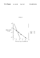
- FIG. 8 is a graphical representation showing the relation between a gate applied voltage and a direct tunnel current
- FIG. 9 is a graphical representation showing the relation between a thickness of a gate oxide film and a direct tunnel current.
- FIG. 10 is a graphical representation showing the relation between a thickness of a gate oxide film and a leakage current.
- the present inventors found out that if the thickness of the gate insulating film in the conventional logic circuit is made thinner than 2.5 nm, then a direct tunnel current is caused to flow through the gate insulating film even in non-operation, and hence the power consumption in the non-operation can be suppressed by reducing this direct tunnel current.
- FIG. 6A is a circuit diagram showing a configuration of an example of a circuit including MOS FETs each having a gate insulating film with a thickness of less than 2.5 nm
- FIG. 6B is a circuit diagram useful in explaining a through current which is generated in the circuit shown in FIG. 6A
- FIG. 6C is a circuit diagram useful in explaining a through current which is generated in the circuit shown in FIG. 6 A.
- FIG. 6A is a circuit diagram showing a configuration of an example of a circuit including MOS FETs each having a gate insulating film with
- the inverter INV 21 includes a p-channel MOS FET P 21 and an n-channel MOS FET N 21
- the inverter INV 22 includes a p-channel MOS FET P 22 and an n-channel MOS FET N 22 .
- Each of the MOS FETs P 21 , P 22 , N 21 and N 22 is the high threshold voltage MOS FET having a high threshold.
- a signal at a low level is output through an output terminal OUT 21 which is connected to both of a drain of the p-channel MOS FET P 22 and a drain of the n-channel MOS FET N 22 .
- the signal which is input to the inverter INV 21 is held at a low level so that the circuit is in a normal (non-operation) state, and also each of the p-channel MOS FET P 21 and the n-channel MOS FET N 21 is the high threshold voltage MOS FET, if the thickness of the gate insulating film is equal to or larger than 2.5 nm, then the current is hardly caused to flow through the path extending from a power source line L 21 to a GND line L 22 .
- the direct tunnel current is caused to flow through the gate insulating film of the n-channel MOS FET N 22 .
- a through current 23 is caused to flow through the path extending from the power source line L 21 to the GND line L 22 .
- the direct tunnel current is caused to flow through the gate insulating film of the p-channel MOS FET P 22 , and hence a through current 24 is caused to flow through the path extending from the power source line L 21 to the GND line L 22 .
- FIG. 7A is a circuit diagram useful in explaining a through current which is caused to flow through a circuit disclosed in Japanese Patent Application Laid-open No. Hei 6-29834 when a thickness of a gate insulating film is made 2.0 nm
- FIG. 7B is a schematic cross sectional view showing the structure of a semiconductor device in which this circuit shown in FIG. 7A is incorporated on a P type semiconductor substrate.
- FIG. 7A includes a p-channel MOS FET P 14 and an n-channel MOS FET N 14 each of which is the high threshold voltage MOS FET.
- a terminal T 11 is connected to a GND line L 14
- a terminal T 12 is connected to a switch SW 11 .
- a terminal T 13 is connected to a pseudo GND line V 12
- a terminal T 14 is connected to an inverter INV 12 .
- a terminal T 15 is connected to a pseudo power source line V 11
- a terminal T 16 is connected to the switch SW 11 through an inverter INV 13 .
- a terminal T 17 is connected to a power source line L 13 .
- both of the n-channel MOS FETs N 11 and N 13 are formed in a P type well 13 which is at the same potential as that of the GND line L 14
- both of the p-channel MOS FETs P 11 and P 13 are formed in an N type well 15 which is at the same potential as that of the power source line L 13
- both of the P type well 13 and the N type well 15 are formed in the same P type semiconductor substrate 11 .
- the pseudo power source line V 11 and the pseudo GND line V 12 are respectively separated from the power source line L 13 and the GND line L 14 by decreasing the amplitude of the input signal to the switch SW 11 to a low level.
- any of through currents such as the through currents 23 and 24 shown in FIGS. 6B and 6C, respectively, is not caused to flow at all.
- the thickness of the gate insulating film is 2.0 nm, and as shown in FIG. 7A, the power source line L 13 is at the same potential as that of the N type well of the p-channel MOS FET P 4 , if a signal at a low level is input to the switch SW 11 , then the direct tunnel current is caused to flow through the gate insulating film of the p-channel MOS FET P 4 , which results in a through current 25 being caused to flow.
- the thickness of the gate insulating film is 2.0 nm, and as shown in FIG.
- the P type well 13 of the n-channel MOS FET N 11 is at the same potential as that of the GND line L 14 connected to the terminal T 11 , if the input signal is held at a high level, then the direct tunnel current is caused to flow through the gate insulating film of the n-channel MOS FET Nil, which results in a through current 26 being caused to flow.
- the direct tunnel current is caused to flow through the gate insulating film of the p-channel MOS FET P 11 , which results in a through current being caused to flow. Since the through current due to the direct tunnel current is different from the through current which is the problem associated with the prior art, in the conventional circuit, even if the switch SW 11 is placed in a nonconducting state, such a through current can not be suppressed.
- FIG. 8 is a graphical representation showing the relation between a gate applied voltage, on the axis of abscissa, which is applied to the gate and a direct tunnel current on the axis of ordinate.
- the direct tunnel current in the inversion state is larger than that in the accumulation state by the amount corresponding to a flat band voltage.
- FIG. 9 is a graphical representation showing the relation between the thickness of the gate oxide film on the axis of abscissa and the direct tunnel current on the axis of ordinate.
- open symbols ⁇ represent the direct tunnel current when the power source voltage is 1.8 V
- black symbols ⁇ represent the direct tunnel current when the power source voltage is 1.2 V.
- the dependency of the direct tunnel current on the thickness of the gate insulating film is very remarkable, and hence whenever the gate insulating film is thinned by 0.2 nm, the direct tunnel current increases by about one digit.
- FIG. 10 is a graphical representation showing the relation between the thickness of the Gate insulating film on the axis of abscissa and the leakage current on the axis of ordinate.
- the gate width of the MOS transistor is 1 ⁇ m.
- open symbols ⁇ represent the leakage current due to the direct tunnel current
- black symbols ⁇ represent the leakage current due to the stand-by current.
- the leakage current due to the direct tunnel current is larger than the stand-by current of the MOS transistor.
- the through current due to the direct tunnel current is the predominant current.
- FIG. 1A is a circuit diagram showing a configuration of a circuit which is incorporated in a complementary MOS semiconductor device according to a first embodiment of the present invention
- FIG. 1B is a schematic cross sectional view showing the structure of the complementary MOS semiconductor device according to the first embodiment of the present invention.
- an internal logic circuit including two-stages inverters INV 1 and INV 2 is incorporated.
- the inverter INV 1 includes a p-channel MOS FET P 1 and an n-channel MOS FET N 1
- the inverter INV 2 includes a p-channel MOS FET P 2 and an n-channel MOS FET N 2 .
- Each of these MOS FETs P 1 , P 2 , N 1 and N 2 is a MOS FET having a gate insulating film with 2 nm thickness.
- the gate insulating film is, for example, formed of a silicon oxide film or a silicon nitride oxide film which is formed by nitriding a silicon oxide film.
- the silicon oxide film is, for example, formed by oxidizing the surface of a silicon substrate by the operation of the nitrogen oxide.
- Sources and a well of the p-channel MOS FETs P 1 and P 2 are connected to a pseudo power source line V 1 .
- sources and a well of the n-channel MOS FETs N 1 and N 2 are connected to a pseudo GND line V 2 .
- a p-channel MOS FET P 3 is connected as a power supply circuit S 1 to the pseudo power source line V 1
- an n-channel MOS FET N 3 is connected as a power supply circuit S 2 to the pseudo GND line V 2
- a power source line L 1 is connected to the power supply circuit S 1
- a GND line L 2 is connected to the power supply circuit S 2
- an inverter INV 3 is connected as a power supply circuit S 3 to a gate of the p-channel MOS FET P 3
- a switch SW 1 is connected to both of the inverter INV 3 and a gate of the n-channel MOS FET N 3 .
- the inverter INV 3 includes a p-channel MOS FET P 4 and an n-channel MOS FET N 4 .
- the p-channel MOS FET P 4 is connected to the power source line L 1
- the n-channel MOS FET N 4 is connected to the GND line L 2 .
- each of the p-channel MOS FET P 4 and the n-channel MOS FET N 4 is a MOS FET having a gate insulating film with 4 nm thickness.
- a terminal T 1 is connected to the GND line L 2 , and a terminal T 2 is connected to the switch SW 1 .
- a terminal T 3 is connected to the pseudo GND line V 2 , and a terminal T 4 is connected to the inverter INV 2 .
- a terminal T 5 is connected to the pseudo power source line V 1 , and a terminal T 6 is connected to the switch SW 1 through the inverter INV 3 .
- a terminal T 7 is connected to the power source line L 1 .
- the n-channel MOS FET N 1 is formed in a first P type well 2
- the n-channel MOS FET N 3 is formed in a second P type well 3
- the first P type well 2 and the second P type well 3 are formed in the same third N type well 4 so as to be located apart from each other.
- the first P type well 2 and the second P type well 3 are electrically insulated from each other.
- the p-channel MOS FET P 1 is formed in a first N type well 5
- the p-channel MOS FET P 3 is formed in a second N type well 6 .
- first N type well 5 , the second N type well 6 and the third N type well 4 are formed in a P type semiconductor substrate 1 so as to be located apart from one another.
- first N type well 5 and the second N type well 6 are electrically insulated from each other.
- a p-channel MOS FET P 2 (not shown in FIG. 1B) may be formed in the same first N type well 5 as that of the p-channel MOS FET P 1 .
- an n-channel MOS FET N 2 (not shown in FIG. 1B) may be formed in the same first P type well 2 as that of the n-channel MOS FET N 1 .
- the switch SW 1 is placed in a nonconducting state in the non-operation of the internal logic circuit including the inverters INV 1 and INV 2 , whereby similarly to the prior art, the internal logic circuit is separated from the power source line L 1 and the GND line L 2 , and hence the power source voltage is not supplied to the internal logic circuit.
- the through current such as the through current 23 or 24 shown in FIG. 6B or FIG. 6C is prevented from being generated.
- the thickness of the gate insulating film of the p-channel MOS FET P 4 is 4 nm, the direct tunnel current is prevented from being generated in the p-channel MOS FET P 4 . This results in the through current such as the through current 25 shown in FIG.
- first P type well 2 and the second P type well 3 are electrically insulated from each other, even when the signal at a high level is held at the input terminal IN 1 , the through current such as the through current 26 shown in FIGS. 7A and 7B is prevented from being generated. Also, since the first N type well 5 and the second N type well 6 are electrically insulated from each other, when the signal at a low level is held at the input terminal IN 1 , the through current is prevented from being caused to flow through the path extending from the input terminal IN 1 to the power source line L 1 .
- the gate insulating films of the p-channel MOS FET P 3 and the n-channel MOS FET N 3 are not limited in thickness. But, if the thickness of the gate insulating film of the p-channel MOS FET P 3 is thinner than 2.5 nm, then a current is caused to flow through the path extending from the power source line L 1 to the gate of the p-channel MOS FET P 3 in the operation of the inverters INV 1 and INV 2 , and if the thickness of the gate insulating film of the n-channel MOS FET N 3 is thinner than 2.5 nm, then a current is caused to flow through the path extending from the gate of the n-channel MOS FET N 3 to the GND line L 2 in the operation of the inverters INV 1 and INV 2 .
- the gate insulating films of the p-channel MOS FET P 3 and the n-channel MOS FET N 3 are desirably equal to or larger than 2.5 nm in thickness.
- FIG. 2 is a schematic cross sectional view showing the structure of a complementary MOS semiconductor device according to the second embodiment of the present invention.
- those parts corresponding to their counter parts of the first embodiment shown in FIG. 1B are denoted by the same reference numerals, and the detailed description thereof is omitted here for the sake of simplicity.
- the first P type well 2 is formed in a third N type well 4 a , while the second P type well 3 is directly formed in the P type semiconductor substrate 1 .
- the first P type well 2 and the second P type well 3 are electrically insulated from each other.
- the direct tunnel current is not caused to flow through the n-channel MOS FET N 1 when the signal at a high level is held at the input terminal IN 1 so that a through current such as the through current 26 shown in FIGS. 7A and 7B is prevented from being generated.
- FIG. 3 is a schematic cross sectional view showing the structure of a complementary MOS semiconductor device according to the third embodiment of the present invention.
- those parts corresponding to their counter parts of the first embodiment shown in FIG. 1B are denoted by the same reference numerals, and the detailed description thereof is omitted here for the sake of simplicity.
- the second P type well 3 is formed in a third N type well 4 b , while the first P type well 2 is directly formed in the P type semiconductor substrate 1 . In such a way, the first P type well 2 and the second P type well 3 are electrically insulated from each other.
- the direct tunnel current is not caused to flow through the n-channel MOS FET N 1 when the signal at a high level is held at the input terminal IN 1 so that a through current such as the through current 26 shown in FIGS. 7A and 7B is prevented from being generated.
- the N type well 4 and the like are required through which the P type wells 2 and 3 are electrically insulated from each other, while when the elements are formed on an N type semiconductor substrate, a P type well is required through which the N type wells 5 and 6 are electrically insulated from each other.
- gate insulating films of field effect transistors which are provided in a power supply circuit are made equal to or larger than 2.5 nm in thickness, whereby it is possible to suppress a direct tunnel current which is caused to flow through the power supply circuit during non-operation of a complementary MOS logic circuit.
- wells of the field effect transistors which are provided in the complementary MOS logic circuit are electrically insulated from a first wiring and a second wiring thereof, whereby it is possible to prevent any of direct tunnel currents from being caused to flow through the path extending therebetween.
Abstract
Description
Claims (9)
Applications Claiming Priority (2)
| Application Number | Priority Date | Filing Date | Title |
|---|---|---|---|
| JP9-313985 | 1997-11-14 | ||
| JP31398597A JP3185730B2 (en) | 1997-11-14 | 1997-11-14 | Complementary MOS semiconductor device |
Publications (1)
| Publication Number | Publication Date |
|---|---|
| US6307234B1 true US6307234B1 (en) | 2001-10-23 |
Family
ID=18047847
Family Applications (1)
| Application Number | Title | Priority Date | Filing Date |
|---|---|---|---|
| US09/190,010 Expired - Lifetime US6307234B1 (en) | 1997-11-14 | 1998-11-12 | Complementary MOS semiconductor device |
Country Status (7)
| Country | Link |
|---|---|
| US (1) | US6307234B1 (en) |
| EP (1) | EP0917201B1 (en) |
| JP (1) | JP3185730B2 (en) |
| KR (1) | KR100274562B1 (en) |
| CN (1) | CN1217578A (en) |
| DE (1) | DE69837242T2 (en) |
| TW (1) | TW402820B (en) |
Cited By (14)
| Publication number | Priority date | Publication date | Assignee | Title |
|---|---|---|---|---|
| US6380594B1 (en) * | 1999-10-19 | 2002-04-30 | Nec Corporation | Semiconductor device |
| US6635934B2 (en) * | 2000-06-05 | 2003-10-21 | Mitsubishi Denki Kabushiki Kaisha | Semiconductor integrated circuit device operating with low power consumption |
| US20040080340A1 (en) * | 2002-10-25 | 2004-04-29 | Mitsubishi Denki Kabushiki Kaisha | Low power consumption MIS semiconductor device |
| US20040079978A1 (en) * | 2002-03-27 | 2004-04-29 | Sung-Mo Kang | Low-power high-performance storage circuitry |
| US20040169201A1 (en) * | 2003-02-27 | 2004-09-02 | Nec Electronics Corporation | Layout structure of multiplexer cells |
| US20050127941A1 (en) * | 2003-12-12 | 2005-06-16 | Matsushita Electric Industrial Co., Ltd. | Semiconductor device |
| US20050190633A1 (en) * | 2001-05-22 | 2005-09-01 | The Regents Of The University Of California | Low-power high-performance integrated circuit and related methods |
| US20060282725A1 (en) * | 2003-09-17 | 2006-12-14 | Martin Kerber | Electronic switching circuit, switching circuit test arrangement and method for determining the operativiness of an electronic switching circuit |
| US20070296488A1 (en) * | 2006-06-21 | 2007-12-27 | Samsung Electronics Co., Ltd. | Semiconductor integrated circuits |
| US20080093632A1 (en) * | 2006-10-19 | 2008-04-24 | Nec Electronics Corporation | Size-reduced layout of cell-based integrated circuit with power switch |
| US7391232B1 (en) * | 2007-10-30 | 2008-06-24 | International Business Machines Corporation | Method and apparatus for extending lifetime reliability of digital logic devices through reversal of aging mechanisms |
| US7391233B1 (en) * | 2007-10-30 | 2008-06-24 | International Business Machines Corporation | Method and apparatus for extending lifetime reliability of digital logic devices through removal of aging mechanisms |
| US20080278194A1 (en) * | 2007-05-11 | 2008-11-13 | Sony Corporation | Semiconductor integrated circuit and operation method of the same |
| TWI418010B (en) * | 2008-11-25 | 2013-12-01 | Nuvoton Technology Corp | Electrostatic discharge protection circuit and device |
Families Citing this family (7)
| Publication number | Priority date | Publication date | Assignee | Title |
|---|---|---|---|---|
| JP2001230664A (en) | 2000-02-15 | 2001-08-24 | Mitsubishi Electric Corp | Semiconductor integrated circuit |
| JP2011228725A (en) * | 2000-06-05 | 2011-11-10 | Renesas Electronics Corp | Semiconductor device |
| US6642583B2 (en) * | 2001-06-11 | 2003-11-04 | Fuji Electric Co., Ltd. | CMOS device with trench structure |
| JP2003110022A (en) * | 2001-09-28 | 2003-04-11 | Mitsubishi Electric Corp | Semiconductor integrated circuit |
| US6639827B2 (en) * | 2002-03-12 | 2003-10-28 | Intel Corporation | Low standby power using shadow storage |
| JP4184104B2 (en) | 2003-01-30 | 2008-11-19 | 株式会社ルネサステクノロジ | Semiconductor device |
| KR101966522B1 (en) * | 2017-05-19 | 2019-04-05 | 안소연 | The whisk for measuring temperature of paste |
Citations (11)
| Publication number | Priority date | Publication date | Assignee | Title |
|---|---|---|---|---|
| US4475050A (en) * | 1981-12-21 | 1984-10-02 | Motorola, Inc. | TTL To CMOS input buffer |
| US4672243A (en) * | 1985-05-28 | 1987-06-09 | American Telephone And Telegraph Company, At&T Bell Laboratories | Zero standby current TTL to CMOS input buffer |
| JPH0629834A (en) | 1991-11-26 | 1994-02-04 | Nippon Telegr & Teleph Corp <Ntt> | Logic circuit |
| JPH06350435A (en) | 1993-06-02 | 1994-12-22 | Nippon Telegr & Teleph Corp <Ntt> | Power down circuit |
| JPH07142605A (en) | 1993-11-22 | 1995-06-02 | Fujitsu Ltd | Semiconductor device and manufacturing method thereof |
| JPH08191107A (en) | 1995-01-11 | 1996-07-23 | Mitsubishi Electric Corp | Semiconductor device and manufacturing method thereof |
| WO1997038444A1 (en) | 1996-04-08 | 1997-10-16 | Hitachi, Ltd. | Semiconductor integrated circuit device |
| US5900665A (en) * | 1997-04-01 | 1999-05-04 | Mitsubishi Denki Kabushiki Kaisha | Semiconductor integrated circuit device operating at high speed with low current consumption |
| US5929667A (en) * | 1997-06-10 | 1999-07-27 | International Business Machines Corporation | Method and apparatus for protecting circuits subjected to high voltage |
| US5985706A (en) * | 1997-05-08 | 1999-11-16 | Advanced Micro Devices, Inc. | Polishing method for thin gates dielectric in semiconductor process |
| US6093947A (en) * | 1998-08-19 | 2000-07-25 | International Business Machines Corporation | Recessed-gate MOSFET with out-diffused source/drain extension |
Family Cites Families (1)
| Publication number | Priority date | Publication date | Assignee | Title |
|---|---|---|---|---|
| JP3071612B2 (en) * | 1993-07-15 | 2000-07-31 | 日本電気株式会社 | CMOS type semiconductor integrated circuit |
-
1997
- 1997-11-14 JP JP31398597A patent/JP3185730B2/en not_active Expired - Fee Related
-
1998
- 1998-11-09 TW TW087118633A patent/TW402820B/en not_active IP Right Cessation
- 1998-11-12 CN CN98124728A patent/CN1217578A/en active Pending
- 1998-11-12 US US09/190,010 patent/US6307234B1/en not_active Expired - Lifetime
- 1998-11-13 EP EP98250397A patent/EP0917201B1/en not_active Expired - Lifetime
- 1998-11-13 KR KR1019980048699A patent/KR100274562B1/en not_active IP Right Cessation
- 1998-11-13 DE DE69837242T patent/DE69837242T2/en not_active Expired - Fee Related
Patent Citations (13)
| Publication number | Priority date | Publication date | Assignee | Title |
|---|---|---|---|---|
| US4475050A (en) * | 1981-12-21 | 1984-10-02 | Motorola, Inc. | TTL To CMOS input buffer |
| US4672243A (en) * | 1985-05-28 | 1987-06-09 | American Telephone And Telegraph Company, At&T Bell Laboratories | Zero standby current TTL to CMOS input buffer |
| JPH0629834A (en) | 1991-11-26 | 1994-02-04 | Nippon Telegr & Teleph Corp <Ntt> | Logic circuit |
| JPH06350435A (en) | 1993-06-02 | 1994-12-22 | Nippon Telegr & Teleph Corp <Ntt> | Power down circuit |
| JPH07142605A (en) | 1993-11-22 | 1995-06-02 | Fujitsu Ltd | Semiconductor device and manufacturing method thereof |
| US5789788A (en) | 1993-11-22 | 1998-08-04 | Fujitsu Limited | Semiconductor device with first and second wells which have opposite conductivity types and a third well region formed on one of the first and second wells |
| US5847432A (en) * | 1995-01-11 | 1998-12-08 | Mitsubishi Denki Kabushiki Kaisha | Semiconductor device and production method therefor |
| JPH08191107A (en) | 1995-01-11 | 1996-07-23 | Mitsubishi Electric Corp | Semiconductor device and manufacturing method thereof |
| WO1997038444A1 (en) | 1996-04-08 | 1997-10-16 | Hitachi, Ltd. | Semiconductor integrated circuit device |
| US5900665A (en) * | 1997-04-01 | 1999-05-04 | Mitsubishi Denki Kabushiki Kaisha | Semiconductor integrated circuit device operating at high speed with low current consumption |
| US5985706A (en) * | 1997-05-08 | 1999-11-16 | Advanced Micro Devices, Inc. | Polishing method for thin gates dielectric in semiconductor process |
| US5929667A (en) * | 1997-06-10 | 1999-07-27 | International Business Machines Corporation | Method and apparatus for protecting circuits subjected to high voltage |
| US6093947A (en) * | 1998-08-19 | 2000-07-25 | International Business Machines Corporation | Recessed-gate MOSFET with out-diffused source/drain extension |
Non-Patent Citations (2)
| Title |
|---|
| Wolf, "Silicon Processing for the VLSI Era," vol. 3, pp. 421-422, 523-524, 1995.* |
| Wright P. J. et al.: Thickness Limitations of SiO2 Gate Dielectrics for MOS ULSI, Aug. 1990, vol. 37, No. 8, pp. 1884-1892. |
Cited By (34)
| Publication number | Priority date | Publication date | Assignee | Title |
|---|---|---|---|---|
| US6380594B1 (en) * | 1999-10-19 | 2002-04-30 | Nec Corporation | Semiconductor device |
| US20050212560A1 (en) * | 2000-06-05 | 2005-09-29 | Renesas Technology Corp. | Semiconductor integrated circuit device operating with low power consumption |
| US6635934B2 (en) * | 2000-06-05 | 2003-10-21 | Mitsubishi Denki Kabushiki Kaisha | Semiconductor integrated circuit device operating with low power consumption |
| US20040071026A1 (en) * | 2000-06-05 | 2004-04-15 | Mitsubishi Denki Kabushiki Kaisha | Semiconductor integrated circuit device operating with low power consumption |
| US7521762B2 (en) | 2000-06-05 | 2009-04-21 | Renesas Technology Corp. | Semiconductor integrated circuit device operating with low power consumption |
| US20090179692A1 (en) * | 2000-06-05 | 2009-07-16 | Renesas Technology Corp. | Semiconductor integrated circuit device operating with low power consumption |
| US6911703B2 (en) | 2000-06-05 | 2005-06-28 | Renesas Technology Corp. | Semiconductor integrated circuit device operating with low power consumption |
| US7190209B2 (en) | 2001-05-22 | 2007-03-13 | The Regents Of The University Of California | Low-power high-performance integrated circuit and related methods |
| US20050190633A1 (en) * | 2001-05-22 | 2005-09-01 | The Regents Of The University Of California | Low-power high-performance integrated circuit and related methods |
| US20040079978A1 (en) * | 2002-03-27 | 2004-04-29 | Sung-Mo Kang | Low-power high-performance storage circuitry |
| US6888202B2 (en) * | 2002-03-27 | 2005-05-03 | The Regents Of The University Of California | Low-power high-performance storage circuitry |
| US20050201144A1 (en) * | 2002-03-27 | 2005-09-15 | The Regents Of The University Of California | Low-power high-performance storage circuitry |
| US7928759B2 (en) | 2002-10-25 | 2011-04-19 | Renesas Electronics Corporation | Low power consumption MIS semiconductor device |
| US7042245B2 (en) | 2002-10-25 | 2006-05-09 | Renesas Technology Corp. | Low power consumption MIS semiconductor device |
| US20060145726A1 (en) * | 2002-10-25 | 2006-07-06 | Renesas Technology Corp. | Low power consumption MIS semiconductor device |
| US20110163779A1 (en) * | 2002-10-25 | 2011-07-07 | Renesas Electronics Corporation | Low power consumption mis semiconductor device |
| US20100219857A1 (en) * | 2002-10-25 | 2010-09-02 | Rensas Technology Corp. | Low power consumption mis semiconductor device |
| US7741869B2 (en) | 2002-10-25 | 2010-06-22 | Renesas Technology Corp. | Low power consumption MIS semiconductor device |
| US7355455B2 (en) | 2002-10-25 | 2008-04-08 | Renesas Technology Corp. | Low power consumption MIS semiconductor device |
| US20080122479A1 (en) * | 2002-10-25 | 2008-05-29 | Renesas Technology Corp. | Low power consumption mis semiconductor device |
| US20040080340A1 (en) * | 2002-10-25 | 2004-04-29 | Mitsubishi Denki Kabushiki Kaisha | Low power consumption MIS semiconductor device |
| US6885045B2 (en) * | 2003-02-27 | 2005-04-26 | Nec Electronics Corporation | Layout structure of multiplexer cells |
| US20040169201A1 (en) * | 2003-02-27 | 2004-09-02 | Nec Electronics Corporation | Layout structure of multiplexer cells |
| US7403026B2 (en) * | 2003-09-17 | 2008-07-22 | Infineon Technologies Ag | Electronic switching circuit, switching circuit test arrangement and method for determining the operativeness of an electronic switching circuit |
| US20060282725A1 (en) * | 2003-09-17 | 2006-12-14 | Martin Kerber | Electronic switching circuit, switching circuit test arrangement and method for determining the operativiness of an electronic switching circuit |
| US7202700B2 (en) * | 2003-12-12 | 2007-04-10 | Matsushita Electric Industrial Co., Ltd. | Semiconductor device which exhibits high-speed performance and low power consumption |
| US20050127941A1 (en) * | 2003-12-12 | 2005-06-16 | Matsushita Electric Industrial Co., Ltd. | Semiconductor device |
| US20070296488A1 (en) * | 2006-06-21 | 2007-12-27 | Samsung Electronics Co., Ltd. | Semiconductor integrated circuits |
| US20080093632A1 (en) * | 2006-10-19 | 2008-04-24 | Nec Electronics Corporation | Size-reduced layout of cell-based integrated circuit with power switch |
| US20080278194A1 (en) * | 2007-05-11 | 2008-11-13 | Sony Corporation | Semiconductor integrated circuit and operation method of the same |
| US7791369B2 (en) * | 2007-05-11 | 2010-09-07 | Sony Corporation | Semiconductor integrated circuit and operation method of the same |
| US7391233B1 (en) * | 2007-10-30 | 2008-06-24 | International Business Machines Corporation | Method and apparatus for extending lifetime reliability of digital logic devices through removal of aging mechanisms |
| US7391232B1 (en) * | 2007-10-30 | 2008-06-24 | International Business Machines Corporation | Method and apparatus for extending lifetime reliability of digital logic devices through reversal of aging mechanisms |
| TWI418010B (en) * | 2008-11-25 | 2013-12-01 | Nuvoton Technology Corp | Electrostatic discharge protection circuit and device |
Also Published As
| Publication number | Publication date |
|---|---|
| TW402820B (en) | 2000-08-21 |
| EP0917201B1 (en) | 2007-03-07 |
| EP0917201A2 (en) | 1999-05-19 |
| DE69837242D1 (en) | 2007-04-19 |
| KR100274562B1 (en) | 2000-12-15 |
| DE69837242T2 (en) | 2007-12-20 |
| KR19990045271A (en) | 1999-06-25 |
| EP0917201A3 (en) | 2000-09-13 |
| CN1217578A (en) | 1999-05-26 |
| JP3185730B2 (en) | 2001-07-11 |
| JPH11150193A (en) | 1999-06-02 |
Similar Documents
| Publication | Publication Date | Title |
|---|---|---|
| US6307234B1 (en) | Complementary MOS semiconductor device | |
| US5461338A (en) | Semiconductor integrated circuit incorporated with substrate bias control circuit | |
| US5559368A (en) | Dynamic threshold voltage mosfet having gate to body connection for ultra-low voltage operation | |
| US5825695A (en) | Semiconductor device for reference voltage | |
| US6741098B2 (en) | High speed semiconductor circuit having low power consumption | |
| US6144080A (en) | Semiconductor integrated circuit device having field shield MOS devices | |
| US6630717B2 (en) | CMOS semiconductor circuit with reverse bias applied for reduced power consumption | |
| US6384639B1 (en) | Circuit and method for reducing static power dissipation in a semiconductor device | |
| US6476641B2 (en) | Low power consuming circuit | |
| WO1999065079A1 (en) | A method of programmability and an architecture for cold sparing of cmos arrays | |
| US6636073B2 (en) | Semiconductor integrated circuit | |
| US5914515A (en) | Semiconductor device | |
| US5815029A (en) | Semiconductor circuit and semiconductor circuit device | |
| US5467048A (en) | Semiconductor device with two series-connected complementary misfets of same conduction type | |
| US6194943B1 (en) | Input circuit protection | |
| JPH0936246A (en) | Semiconductor device | |
| JP2978346B2 (en) | Input circuit of semiconductor integrated circuit device | |
| US5966038A (en) | Circuit with overvoltage protection | |
| JP3144370B2 (en) | Semiconductor device | |
| JP2004289107A (en) | Semiconductor integrated circuit device | |
| JP2000269432A (en) | Semiconductor integrated circuit | |
| KR100271207B1 (en) | High speed and low electric power fet with subsidiary mosfet | |
| KR19980078109A (en) | Static electricity protection circuit of semiconductor device | |
| JPH11150449A (en) | Hysteresis input circuit | |
| JP2786152B2 (en) | Semiconductor integrated circuit device |
Legal Events
| Date | Code | Title | Description |
|---|---|---|---|
| AS | Assignment |
Owner name: NEC CORPORATION, JAPAN Free format text: ASSIGNMENT OF ASSIGNORS INTEREST;ASSIGNORS:ITO, HIROSHI;SASAKI, MAKOTO;REEL/FRAME:009627/0374 Effective date: 19980901 |
|
| STCF | Information on status: patent grant |
Free format text: PATENTED CASE |
|
| FEPP | Fee payment procedure |
Free format text: PAYOR NUMBER ASSIGNED (ORIGINAL EVENT CODE: ASPN); ENTITY STATUS OF PATENT OWNER: LARGE ENTITY |
|
| FPAY | Fee payment |
Year of fee payment: 4 |
|
| FPAY | Fee payment |
Year of fee payment: 8 |
|
| AS | Assignment |
Owner name: RENESAS ELECTRONICS CORPORATION, JAPAN Free format text: CHANGE OF NAME;ASSIGNOR:NEC ELECTRONICS CORPORATION;REEL/FRAME:025185/0597 Effective date: 20100401 |
|
| FPAY | Fee payment |
Year of fee payment: 12 |
|
| AS | Assignment |
Owner name: RENESAS ELECTRONICS CORPORATION, JAPAN Free format text: CHANGE OF ADDRESS;ASSIGNOR:RENESAS ELECTRONICS CORPORATION;REEL/FRAME:044928/0001 Effective date: 20150806 |