US6151561A - Method of estimating lifetime of floating SOI-MOSFET - Google Patents
Method of estimating lifetime of floating SOI-MOSFET Download PDFInfo
- Publication number
- US6151561A US6151561A US09/395,989 US39598999A US6151561A US 6151561 A US6151561 A US 6151561A US 39598999 A US39598999 A US 39598999A US 6151561 A US6151561 A US 6151561A
- Authority
- US
- United States
- Prior art keywords
- mosfet
- soi
- lifetime
- isub
- floating
- Prior art date
- Legal status (The legal status is an assumption and is not a legal conclusion. Google has not performed a legal analysis and makes no representation as to the accuracy of the status listed.)
- Expired - Fee Related
Links
Images


Classifications
-
- H—ELECTRICITY
- H01—ELECTRIC ELEMENTS
- H01L—SEMICONDUCTOR DEVICES NOT COVERED BY CLASS H10
- H01L22/00—Testing or measuring during manufacture or treatment; Reliability measurements, i.e. testing of parts without further processing to modify the parts as such; Structural arrangements therefor
-
- G—PHYSICS
- G01—MEASURING; TESTING
- G01R—MEASURING ELECTRIC VARIABLES; MEASURING MAGNETIC VARIABLES
- G01R31/00—Arrangements for testing electric properties; Arrangements for locating electric faults; Arrangements for electrical testing characterised by what is being tested not provided for elsewhere
- G01R31/26—Testing of individual semiconductor devices
- G01R31/2642—Testing semiconductor operation lifetime or reliability, e.g. by accelerated life tests
-
- G—PHYSICS
- G01—MEASURING; TESTING
- G01R—MEASURING ELECTRIC VARIABLES; MEASURING MAGNETIC VARIABLES
- G01R31/00—Arrangements for testing electric properties; Arrangements for locating electric faults; Arrangements for electrical testing characterised by what is being tested not provided for elsewhere
- G01R31/26—Testing of individual semiconductor devices
- G01R31/2607—Circuits therefor
- G01R31/2621—Circuits therefor for testing field effect transistors, i.e. FET's
Definitions
- the present invention relates to methods of estimating the lifetime of a transistor degraded by hot carriers in an MOSFET and, more particularly, to a method of estimating the lifetime of a floating SOI-MOSFET.
- the lifetime of the transistor degraded by hot carriers can be estimated by measuring a substrate current Isub.
- FIG. 21 schematically shows a cross sectional structure of a typical bulk N-channel MOSFET.
- a source 2 and a drain 3 are formed at one main surface of a semiconductor substrate 1.
- a gate electrode 5 is formed between source 2 and drain 3 on substrate 1 with a gate insulating film 4 interposed therebetween.
- Substrate 1 and source 2 are connected to ground, and a drain voltage Vd is applied to drain 3 and a gate voltage Vg is applied to gate electrode 5.
- the lifetime of a transistor degraded by hot carriers can be estimated by measuring the substrate current.
- FIG. 22 schematically shows a cross sectional structure of a typical SOI-MOSFET.
- a buried insulating layer 6 and a semiconductor layer 1A are stacked on semiconductor substrate 1 in this order.
- semiconductor layer 1A is isolated from substrate 1 by buried insulating layer 6 and semiconductor layer 1A corresponds to substrate 1 in the bulk MOSFET shown in FIG. 21.
- Source 2 and drain 3 are formed in semiconductor layer 1A.
- the region of semiconductor layer 1A excluding source 2 and drain 3 is called a body region 1B.
- gate electrode 5 is formed on semiconductor layer 1A with gate insulating film 4 interposed therebetween.
- Source 2 is connected to ground, drain voltage Vd is applied to drain 3 and gate voltage Vg is applied to gate electrode 5.
- holes "h” produced by impact ionization tend to accumulate in body region 1B, since body region 1B is isolated from substrate 1 by buried insulating layer 6, thereby increasing the potential of the body region.
- Increase in potential in body region 1B turns on an NPN bipolar transistor formed by source 2, body region 1B and drain 3, thereby further increasing the current between source 2 and drain 3 (parasitic bipolar effect).
- the current increased by such parasitic bipolar effect leads to an increase in production of hot carriers to accelerate degradation in transistor characteristics.
- parasitic bipolar effect also makes it difficult to estimate the lifetime of an SOI-MOSFET degraded by hot carriers.
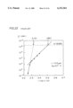
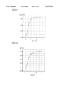
- FIG. 23 is a graph showing the results obtained by measuring the lifetime of the SOI-MOSFET as shown in FIG. 22.
- the reciprocal 1/Vd(1/V) of the drain current is represented on the horizontal axis and the lifetime ⁇ (sec) of the transistor is represented on a log scale on the vertical axis.
- the measured SOI-MOSFET has a channel length L of 0.3 ⁇ m and gate voltage Vg of 0.7V is applied thereto as the hot carrier stress condition.
- the lifetime of the transistor sharply declines in the region with greater drain voltage Vd (the left region of the graph).
- Vd the left region of the graph
- drain voltage Vd allowed for the SOI-MOSFET to have the lifetime of ten years is 3.13V or lower if estimated from the two leftmost measurement points in the graph, but is 1.96V or lower if estimated from the four measurement points on the right side of the graph.
- plotting of the transistor lifetime presents in good linearity in the region with a relatively small drain voltage, measurement of the transistor lifetime in such region requires a long stress test of approximately 10 4 -10 6 seconds, preventing achievement of a simple lifetime estimation method.
- an object of the present invention is to provide a method of estimating the lifetime of a floating SOI-MOSFET simply and accurately.
- the method of estimating the lifetime of a floating SOI-MOSFET includes the steps of:
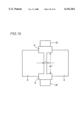
- FIG. 1 is a schematic top plan view showing one example of a body-fixed SOI-MOSFET used for measurement in a method of estimating the lifetime of a floating SOI-MOSFET according to the present invention.
- FIG. 2 is a graph showing one example of determining the lifetime of an SOI-MOSFET by hot carrier stress.
- FIG. 3 is a graph showing the relation between Isub/Id t and ⁇ t ⁇ Id t /W t measured in the body-fixed SOI-MOSFET.
- FIG. 4 is a graph showing the relation between drain voltage Vd and substrate current Isub in the body-fixed SOI-MOSFET.
- FIG. 5 is a graph showing the relation between drain voltage Vd and drain current Id t in the body-fixed SOI-MOSFET.
- FIG. 6 is a schematic top plan view showing one example of a floating SOI-MOSFET.
- FIG. 7 is a schematic top plan view showing another example of a floating SOI-MOSFET.
- FIG. 8 is a graph showing the relation between drain voltage Vd and drain current Id f in the floating SOI-MOSFET.
- FIG. 9 is a graph showing the relation between the reciprocal 1/Vd of the drain voltage and HC lifetime ⁇ f in the floating SOI-MOSFET.
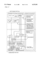
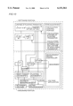
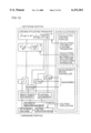
- FIG. 10 is a flow chart showing the procedure in a method of estimating the lifetime of a floating SOI-MOSFET according to a first embodiment of the present invention.
- FIG. 11 is a graph showing the relation between gate voltage Vg and substrate current Isub in the body-fixed SOI-MOSFET.
- FIG. 12 is a graph showing the relation between gate voltage Vg and drain current Id t in the body-fixed SOI-MOSFET.
- FIG. 13 is a graph showing the relation between gate voltage Vg and drain current Id f in the floating SOI-MOSFET.
- FIG. 14 is a graph showing the relation between gate voltage Vg and HC lifetime ⁇ f in the floating SOI-MOSFET.
- FIG. 15 is a flow chart showing the procedure in a method of estimating the lifetime of a floating SOI-MOSFET according to a second embodiment of the present invention.
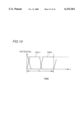
- FIG. 16 is a schematic top plan view showing the relation between a channel length L t and a channel width W t in the SOI-MOSFET.
- FIGS. 17 and 18 are flow charts showing the procedure in methods of estimating the lifetime of a floating SOI-MOSFET according to third and fourth embodiments of the present invention, respectively.
- FIG. 19 is a graph showing one example of periodic stress condition in an SOI-MOSFET incorporated in an IC.
- FIG. 20 is a flow chart showing the procedure in a method of estimating the lifetime of a floating SOI-MOSFET according to a fifth embodiment of the present invention.
- FIG. 21 is a schematic cross sectional view for use in description of estimation of the lifetime of a conventional bulk MOSFET.
- FIG. 22 is a schematic cross sectional view showing the behavior of hot carriers produced by impact ionization in a floating SOI-MOSFET.
- FIG. 23 is a graph showing a conventional method of estimating the lifetime of a floating SOI-MOSFET.
- the method of estimating the lifetime of an SOI-MOSFET according to the present invention is based on the following principle.
- the lifetime of a transistor (hereinafter referred to also as the "HC lifetime") degraded by hot carrier stress can be estimated by measuring substrate current Isub produced by holes from impact ionization occurring in the vicinity of the drain.
- substrate current Isub produced by holes from impact ionization occurring in the vicinity of the drain.
- the HC lifetime can be estimated similarly to the bulk MOSFET if current Ih f produced by holes which are generated as a result of impact ionization occurring in the vicinity of the drain can be estimated.
- Id f represents the drain current in the floating SOI-MOSFET
- Id and Isub represent the drain current and the substrate current in a body-fixed SOI-MOSFET, respectively. Therefore, the lifetime of a floating SOI-MOSFET can be estimated using Ih f in the equation (1) in place of Isub in the equation for estimating the lifetime of an SOI-MOSFET having a body region with a fixed potential.
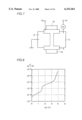
- FIG. 1 is a schematic top plan view showing an example of a body-fixed SOI-MOSFET.
- gate electrode 5 is formed to have an H-shape so that a body electrode 1B adjacent to gate electrode 5 can be provided.
- Substrate current Isub can be measured also in an SOI-MOSFET by using body electrode 1B, and this substrate current Isub, therefore, enables measurement of the HC lifetime of a body-fixed SOI-MOSFET similarly to a bulk MOSFET. It should be noted that the present invention attempts to estimate the lifetime of a floating SOI-MOSFET as shown in FIG. 22, not the lifetime of a body-fixed SOI-MOSFET as shown in FIG. 1.
- substrate currents Isub 1 , and Isub 2 and drain currents Id 1 t and Id 2 t are measured by two ammeters A1 and A2 corresponding to at least two stress conditions S 1 and S 2 for a body-fixed SOI-MOSFET as shown in FIG. 1 by hot carrier stress test. Then, HC lifetime ⁇ t of the body-fixed SOI-MOSFET is obtained under such at least two stress conditions S 1 and S 2 .
- FIG. 2 is a graph representing a method of determining HC lifetime ⁇ t of the body-fixed SOI-MOSFET.
- hot carrier stress time (sec) is scaled on the horizontal axis and shifted amount
- (%) of the transistor parameter is scaled on the vertical axis. Shifted amount ⁇ Vth of the threshold voltage may also be used as the shifted amount of the transistor parameter.
- transistor lifetime ⁇ t is determined when the transistor parameter is shifted to a predetermined ratio (criterion). For example, as shown in FIG.
- lifetime ⁇ t is determined when amount ⁇ Id t of reduction in drain current Id t reaches 15% of initial drain current Id 0 t .
- lives ⁇ t and ⁇ 2 t are determined corresponding to at least two stress conditions S 1 and S 2 described above.
- a graph as shown in FIG. 3 is drawn using drain current Id t , substrate current Isub, and HC lifetime ⁇ t for the body-fixed SOI-MOSFET obtained in the first step.
- Isub/Id t is represented on the horizontal axis
- ⁇ t ⁇ Id t /W t is represented on the vertical axis.
- W t represents the known channel width of the body-fixed SOI-MOSFET.
- Constants A and B are determined so that the following equation (2) fits the straight line in the graph of FIG. 3 (IEEE Transaction on Electron Devices, Vol. ED-32, No. 2, 1955, pp. 375-385): ##EQU4##
- drain voltage dependency Isub(Vd) of the substrate current is measured in the transistor shown in FIG. 1.
- the graph shown in FIG. 4 represents one example of the measurement results.
- drain voltage Vd(V) is scaled on the horizontal axis and substrate current Isub(V) is scaled on the vertical axis.
- gate voltage Vg is maintained at a fixed level and drain voltage Vd t is altered from 0V to 4V.
- the measurement of FIG. 4 can also be utilized for obtaining substrate currents Isub 1 and Isub 2 under different stress conditions in the step 1 described above.
- drain voltage dependency Id t (Vd) of the drain current is measured at the transistor shown in FIG. 1.
- Vg is kept constant and Vd is altered from 0V to 4V as in the case shown in FIG. 4.
- FIG. 5 shows the relationship between Id t and Vd obtained as a result of the measurement.
- Drain voltage dependency Id f (Vd) of the drain current is measured using a floating SOI-MOSFET.
- a floating SOI-MOSFET which does not have a body terminal as shown in FIG. 6 can be employed or the transistor with body terminal 1B in the floating state as shown in FIG. 7 can be used.
- gate voltage Vg is maintained at a fixed level and drain voltage Vd is altered from 0V to 4V as in the case shown in FIG. 4.
- FIG. 8 shows the relationship between Id f and Vd as an example of the result of such measurement.
- HC lifetime ⁇ f (Vd) of the floating SOI-MOSFET can be estimated from the following equation (3) using A, B, Isub(Vd), Id(Vd) and Id f (Vd) obtained from the steps above: ##EQU5##
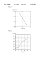
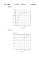
- FIG. 9 is a graph showing the relationship between the HC lifetime actually measured in the floating SOI-MOSFET and the HC lifetime estimated in accordance with the first embodiment of the present invention.
- the circle in the figure represents the actually measured HC lifetime and the broken curve represents the HC lifetime estimated in accordance with the first embodiment of the present invention.
- the transistor lifetime actually measured and the transistor lifetime estimated in accordance with the present invention match well both in the high Vd region (left side of the graph) and the low Vd region (right side of the graph). Therefore, the HC lifetime of a floating SOI-MOSFET can be accurately estimated only by measuring the HC lifetime of a body-fixed SOI-MOSFET.
- FIG. 10 is a flow chart representing the procedure for estimating the lifetime of a floating SOI-MOSFET in accordance with the first embodiment described above.
- the procedure in the method of estimating the lifetime of a floating SOI-MOSFET using the equation (3) should be visually and more clearly understood from this figure.
- the method of estimating the transistor lifetime described above can be applied to a bulk MOSFET having a substrate or a well in the floating state.
- the method can be similarly applied to estimation of the HC lifetime of a TFT (Thin Film Transistor) having no body electrode.
- gate voltage dependency Isub(Vg) of the substrate current is measured using the body-fixed SOI-MOSFET as shown in FIG. 1.
- drain voltage Vd is fixed and gate voltage Vg is altered from 0V to 3.0V.
- FIG. 11 One example of the result of measurement is represented in FIG. 11.
- gate voltage dependency Id t (Vg) of the drain current is measured using the body-fixed SOI-MOSFET as shown in FIG. 1.
- drain voltage Vd is set at a fixed voltage and gate voltage Vg is altered from 0V to 3.0V as in the case shown in FIG. 11.
- FIG. 12 One example of the measurement result is represented in FIG. 12.
- gate voltage dependency Id f (Vg) of the drain current is measured using the floating SOI-MOSFET as shown in FIG. 9 or FIG. 10. Similarly to the case shown in FIG. 11, drain voltage Vd is set at a fixed voltage and gate voltage Vg is changed from 0V to 3.0V.
- FIG. 13 One example of the measurement result is represented in FIG. 13.
- the lifetime of the floating SOI-MOSFET is estimated in accordance with the following equation (4) using A, B, Isub(Vg), Id t (Vg), and Id f (Vg) obtained from the steps above: ##EQU6##
- FIG. 14 shows gate voltage dependency ⁇ f (Vg) of the lifetime of the floating SOI-MOSFET thus derived, and the value of gate voltage Vg with which the lifetime of the floating SOI-MOSFET is shortest can be easily known from this figure.
- FIG. 15 is a flow chart representing the procedure in the method of estimating the lifetime of a floating SOI-MOSFET in accordance with the second embodiment described above.
- the procedure in the method of estimating the lifetime of a floating SOI-MOSFET using the equation (4) should be clarified visually from this figure.
- Equation (5) can be employed instead of the fourth step in the first and second embodiments: ##EQU7## where S represents a predetermined stress condition. S corresponds to Vd in the first embodiment and to Vg in the second embodiment. However, source voltage V s or voltage V back of substrate 1 under buried oxide layer 6 can be used as such stress condition.
- channel length L t and channel width W t as shown in FIG. 16 desirably satisfy the relationship of W t /L t ⁇ 15.
- channel width W t is set equal to or less than 5 ⁇ m with channel length L t of 0.35 ⁇ m. In a floating SOI-MOSFET, however, the value of channel width W f does not matter.
- FIG. 17 is a flow chart representing the procedure in the method of estimating the lifetime of a floating SOI-MOSFET in accordance with the third embodiment described above. The figure should clearly illustrate the procedure in the method of estimating the lifetime of a floating SOI-MOSFET using the equation (5).
- m can be obtained through device simulation and is generally in the range of 0.8-1.0, and m is a constant equal to 0.9 approximately in a typical SOI-MOSFET.
- the lifetime of a floating SOI-MOSFET can be calculated more accurately from the following equation (7) using such coefficient m: ##EQU8##
- m is assumed equal to 1 in the first through third embodiments described above.
- FIG. 18 is a flow chart representing the procedure in the method of estimating the lifetime of a floating SOI-MOSFET in accordance with the fourth embodiment described above.
- the procedure in the method of estimating the lifetime of a floating SOI-MOSFET using the equation (7) should be visually and more clearly understood from this figure.
- the lifetime of the floating SOI-MOSFET in the IC affected by AC stress can be obtained from the following equation (9): ##EQU9## where D is a constant and Tc represents the period of change in time-varying stress condition S(t). Furthermore n can be obtained by measuring the time dependency of transistor parameter ⁇ in the equation (8).
- FIG. 19 shows time dependency Vg(t) of the gate voltage and time dependency Vd(t) of the drain voltage has one example of periodic stress condition S(t).
- S(t) periodic stress condition
- the periodic stress condition Vd(t) and Vg(t) at the SOI-MOSFET in an IC can be obtained from circuit simulation.
- the approximate values can be derived from simple waves such as sine function and rectangular wave, instead of circuit simulation.
- FIG. 20 is a flow chart representing the procedure in the method of estimating the lifetime of a floating SOI-MOSFET in accordance with the fifth embodiment described above.
- the method of estimating the lifetime of a floating SOI-MOSFET utilizing the equation (9) should be visually and more clearly understood from this figure.
- the present invention can provide a method of relatively easily and accurately estimating the lifetime of a floating SOI-MOSFET affected by hot carrier stress.
Abstract
In a method of estimating the lifetime of a floating SOI-MOSFET, constants A and B, stress condition dependency Idt (S) of a drain current and stress condition dependency Isub(S) of a substrate current in a body-fixed SOI-MOSFET, and stress condition dependency Idf (S) of a drain current in the floating SOI-MOSFET are obtained from experiment to estimate lifetime τf (S) from the following equation: ##EQU1## where Wf represents a known channel width of the floating SOI-MOSFET.
Description
This application is a divisional of application Ser. No. 08/709,079 filed Sep. 6, 1996.
1. Field of the Invention
The present invention relates to methods of estimating the lifetime of a transistor degraded by hot carriers in an MOSFET and, more particularly, to a method of estimating the lifetime of a floating SOI-MOSFET.
2. Description of the Background Arts
In a bulk MOSFET, the lifetime of the transistor degraded by hot carriers can be estimated by measuring a substrate current Isub.
FIG. 21 schematically shows a cross sectional structure of a typical bulk N-channel MOSFET. In the MOSFET shown in FIG. 21, a source 2 and a drain 3 are formed at one main surface of a semiconductor substrate 1. A gate electrode 5 is formed between source 2 and drain 3 on substrate 1 with a gate insulating film 4 interposed therebetween. Substrate 1 and source 2 are connected to ground, and a drain voltage Vd is applied to drain 3 and a gate voltage Vg is applied to gate electrode 5.
In such bulk MOSFET, flow of electrons "e" through the channel region from source 2 to drain 3 may cause impact ionization as indicated by a star near drain 3. Impact ionization produces pairs of hole "h" and electron "e" which is the hot carrier with high energy. Holes "h" diffuse in substrate 1 and leave substrate 1 as substrate current Isub through a substrate electrode (or a well electrode). Substrate current Isub can be measured with an ammeter A as shown in FIG. 21.
Meanwhile, electrons "e" or hot carriers penetrate into gate insulating film 4, where they may be trapped or produce an interface state between the channel region and the gate insulating film. Such hot carriers degrade the transistor characteristics.
As can be seen from the foregoing, there is a close correlation between the substrate current and hot carriers since the substrate current is generated by hot carriers produced due to impact ionization in the vicinity of the drain. Therefore, the lifetime of a transistor degraded by hot carriers can be estimated by measuring the substrate current.
FIG. 22 schematically shows a cross sectional structure of a typical SOI-MOSFET. In this SOI-MOSFET, a buried insulating layer 6 and a semiconductor layer 1A are stacked on semiconductor substrate 1 in this order. In the SOI-MOSFET, semiconductor layer 1A is isolated from substrate 1 by buried insulating layer 6 and semiconductor layer 1A corresponds to substrate 1 in the bulk MOSFET shown in FIG. 21. Source 2 and drain 3 are formed in semiconductor layer 1A. The region of semiconductor layer 1A excluding source 2 and drain 3 is called a body region 1B. Between source 2 and drain 3, gate electrode 5 is formed on semiconductor layer 1A with gate insulating film 4 interposed therebetween. Source 2 is connected to ground, drain voltage Vd is applied to drain 3 and gate voltage Vg is applied to gate electrode 5.
As apparent from FIG. 22, generally there is no such thing as a substrate electrode in an SOI-MOSFET. Therefore, in general the lifetime of a transistor degraded by hot carriers cannot be estimated from the substrate current.
It is also understood from FIG. 22 that holes "h" produced by impact ionization tend to accumulate in body region 1B, since body region 1B is isolated from substrate 1 by buried insulating layer 6, thereby increasing the potential of the body region. Increase in potential in body region 1B turns on an NPN bipolar transistor formed by source 2, body region 1B and drain 3, thereby further increasing the current between source 2 and drain 3 (parasitic bipolar effect). The current increased by such parasitic bipolar effect leads to an increase in production of hot carriers to accelerate degradation in transistor characteristics. Thus, such parasitic bipolar effect also makes it difficult to estimate the lifetime of an SOI-MOSFET degraded by hot carriers.
FIG. 23 is a graph showing the results obtained by measuring the lifetime of the SOI-MOSFET as shown in FIG. 22. In this graph, the reciprocal 1/Vd(1/V) of the drain current is represented on the horizontal axis and the lifetime τ(sec) of the transistor is represented on a log scale on the vertical axis. The measured SOI-MOSFET has a channel length L of 0.3 μm and gate voltage Vg of 0.7V is applied thereto as the hot carrier stress condition. As can be seen from FIG. 23, the lifetime of the transistor sharply declines in the region with greater drain voltage Vd (the left region of the graph). Thus, since plotting of the transistor lifetime does not result in a straight line, accurate estimation of the lifetime of the SOI-MOSFET is difficult. For example, drain voltage Vd allowed for the SOI-MOSFET to have the lifetime of ten years is 3.13V or lower if estimated from the two leftmost measurement points in the graph, but is 1.96V or lower if estimated from the four measurement points on the right side of the graph. Although plotting of the transistor lifetime presents in good linearity in the region with a relatively small drain voltage, measurement of the transistor lifetime in such region requires a long stress test of approximately 104 -106 seconds, preventing achievement of a simple lifetime estimation method.
In view of the problems as described above, an object of the present invention is to provide a method of estimating the lifetime of a floating SOI-MOSFET simply and accurately.
The method of estimating the lifetime of a floating SOI-MOSFET includes the steps of:
deriving, corresponding to at least two stress conditions S1 and S2, substrate currents Isub1, and Isub2, drain currents Id1 t and Id2 t, and transistor lives τ1 t and τ2 t from hot carrier stress test for a body-fixed SOI-MOSFET;
using at least Isub1, Isub2, Id1 t, Id2 t, τ1 t and τ2 t to determine constants A and B in the following equation (2) ##EQU2## which equation includes a channel width Wt of the body-fixed SOI-MOSFET;
deriving, from measurement, stress condition dependency Isub(S) of the substrate current and stress condition dependency Idt (S) of the drain current for the body-fixed SOI-MOSFET, and deriving, from measurement, stress condition dependency Idf (S) of the floating SOI-MOSFET; and
using A, B, Isub(S), Idt (S), and Idf (S) to calculate a lifetime τf (S) of the floating SOI-MOSFET under arbitrary stress conditions from the following equation (5) ##EQU3## which equation includes the known channel width Wf of the floating SOI-MOSFET.
The foregoing and other objects, features, aspects and advantages of the present invention will become more apparent from the following detailed description of the present invention when taken in conjunction with the accompanying drawings.
FIG. 1 is a schematic top plan view showing one example of a body-fixed SOI-MOSFET used for measurement in a method of estimating the lifetime of a floating SOI-MOSFET according to the present invention.
FIG. 2 is a graph showing one example of determining the lifetime of an SOI-MOSFET by hot carrier stress.
FIG. 3 is a graph showing the relation between Isub/Idt and τt ·Idt /Wt measured in the body-fixed SOI-MOSFET.
FIG. 4 is a graph showing the relation between drain voltage Vd and substrate current Isub in the body-fixed SOI-MOSFET.
FIG. 5 is a graph showing the relation between drain voltage Vd and drain current Idt in the body-fixed SOI-MOSFET.
FIG. 6 is a schematic top plan view showing one example of a floating SOI-MOSFET.
FIG. 7 is a schematic top plan view showing another example of a floating SOI-MOSFET.
FIG. 8 is a graph showing the relation between drain voltage Vd and drain current Idf in the floating SOI-MOSFET.
FIG. 9 is a graph showing the relation between the reciprocal 1/Vd of the drain voltage and HC lifetime τf in the floating SOI-MOSFET.
FIG. 10 is a flow chart showing the procedure in a method of estimating the lifetime of a floating SOI-MOSFET according to a first embodiment of the present invention.
FIG. 11 is a graph showing the relation between gate voltage Vg and substrate current Isub in the body-fixed SOI-MOSFET.
FIG. 12 is a graph showing the relation between gate voltage Vg and drain current Idt in the body-fixed SOI-MOSFET.
FIG. 13 is a graph showing the relation between gate voltage Vg and drain current Idf in the floating SOI-MOSFET.
FIG. 14 is a graph showing the relation between gate voltage Vg and HC lifetime τf in the floating SOI-MOSFET.
FIG. 15 is a flow chart showing the procedure in a method of estimating the lifetime of a floating SOI-MOSFET according to a second embodiment of the present invention.
FIG. 16 is a schematic top plan view showing the relation between a channel length Lt and a channel width Wt in the SOI-MOSFET.
FIGS. 17 and 18 are flow charts showing the procedure in methods of estimating the lifetime of a floating SOI-MOSFET according to third and fourth embodiments of the present invention, respectively.
FIG. 19 is a graph showing one example of periodic stress condition in an SOI-MOSFET incorporated in an IC.
FIG. 20 is a flow chart showing the procedure in a method of estimating the lifetime of a floating SOI-MOSFET according to a fifth embodiment of the present invention.
FIG. 21 is a schematic cross sectional view for use in description of estimation of the lifetime of a conventional bulk MOSFET.
FIG. 22 is a schematic cross sectional view showing the behavior of hot carriers produced by impact ionization in a floating SOI-MOSFET.
FIG. 23 is a graph showing a conventional method of estimating the lifetime of a floating SOI-MOSFET.
The method of estimating the lifetime of an SOI-MOSFET according to the present invention is based on the following principle.
As described above, in a bulk MOSFET as shown in FIG. 21, the lifetime of a transistor (hereinafter referred to also as the "HC lifetime") degraded by hot carrier stress can be estimated by measuring substrate current Isub produced by holes from impact ionization occurring in the vicinity of the drain. Meanwhile, in a floating SOI-MOSFET as shown in FIG. 22, there is no substrate current Isub, but the HC lifetime can be estimated similarly to the bulk MOSFET if current Ihf produced by holes which are generated as a result of impact ionization occurring in the vicinity of the drain can be estimated.
The present inventors have found as a result of studies that an approximate value of hole current Ihf can be obtained by the following equation (1):
Ih.sup.f ≈(Id.sup.f /Id.sup.t)Isub
where Idf represents the drain current in the floating SOI-MOSFET, and Id and Isub represent the drain current and the substrate current in a body-fixed SOI-MOSFET, respectively. Therefore, the lifetime of a floating SOI-MOSFET can be estimated using Ihf in the equation (1) in place of Isub in the equation for estimating the lifetime of an SOI-MOSFET having a body region with a fixed potential.
FIG. 1 is a schematic top plan view showing an example of a body-fixed SOI-MOSFET. Referring to FIG. 1, gate electrode 5 is formed to have an H-shape so that a body electrode 1B adjacent to gate electrode 5 can be provided. Substrate current Isub can be measured also in an SOI-MOSFET by using body electrode 1B, and this substrate current Isub, therefore, enables measurement of the HC lifetime of a body-fixed SOI-MOSFET similarly to a bulk MOSFET. It should be noted that the present invention attempts to estimate the lifetime of a floating SOI-MOSFET as shown in FIG. 22, not the lifetime of a body-fixed SOI-MOSFET as shown in FIG. 1.
In a first embodiment of the present invention, as a first step, substrate currents Isub1, and Isub2 and drain currents Id1 t and Id2 t are measured by two ammeters A1 and A2 corresponding to at least two stress conditions S1 and S2 for a body-fixed SOI-MOSFET as shown in FIG. 1 by hot carrier stress test. Then, HC lifetime τt of the body-fixed SOI-MOSFET is obtained under such at least two stress conditions S1 and S2.
FIG. 2 is a graph representing a method of determining HC lifetime τt of the body-fixed SOI-MOSFET. In this graph, hot carrier stress time (sec) is scaled on the horizontal axis and shifted amount |ΔIdt /Id0 t |(%) of the transistor parameter is scaled on the vertical axis. Shifted amount ΔVth of the threshold voltage may also be used as the shifted amount of the transistor parameter. In the graph as shown in FIG. 2, transistor lifetime τt is determined when the transistor parameter is shifted to a predetermined ratio (criterion). For example, as shown in FIG. 2, lifetime τt is determined when amount ΔIdt of reduction in drain current Idt reaches 15% of initial drain current Id0 t. Thus, lives τt and τ2 t are determined corresponding to at least two stress conditions S1 and S2 described above.
As a second step, a graph as shown in FIG. 3 is drawn using drain current Idt, substrate current Isub, and HC lifetime τt for the body-fixed SOI-MOSFET obtained in the first step. In the graph shown in FIG. 3, Isub/Idt is represented on the horizontal axis and τt ·Idt /Wt is represented on the vertical axis. Here, Wt represents the known channel width of the body-fixed SOI-MOSFET. In FIG. 3, measurement results under three stress conditions are plotted. Constants A and B are determined so that the following equation (2) fits the straight line in the graph of FIG. 3 (IEEE Transaction on Electron Devices, Vol. ED-32, No. 2, 1955, pp. 375-385): ##EQU4##
As a third step, drain voltage dependency Isub(Vd) of the substrate current is measured in the transistor shown in FIG. 1. The graph shown in FIG. 4 represents one example of the measurement results. In this graph, drain voltage Vd(V) is scaled on the horizontal axis and substrate current Isub(V) is scaled on the vertical axis. In the measurement of FIG. 4, gate voltage Vg is maintained at a fixed level and drain voltage Vdt is altered from 0V to 4V. The measurement of FIG. 4 can also be utilized for obtaining substrate currents Isub1 and Isub2 under different stress conditions in the step 1 described above.
Similarly, drain voltage dependency Idt (Vd) of the drain current is measured at the transistor shown in FIG. 1. In this case as well, Vg is kept constant and Vd is altered from 0V to 4V as in the case shown in FIG. 4. FIG. 5 shows the relationship between Idt and Vd obtained as a result of the measurement.
Drain voltage dependency Idf (Vd) of the drain current is measured using a floating SOI-MOSFET. For this measurement, a floating SOI-MOSFET which does not have a body terminal as shown in FIG. 6 can be employed or the transistor with body terminal 1B in the floating state as shown in FIG. 7 can be used. In this measurement as well, gate voltage Vg is maintained at a fixed level and drain voltage Vd is altered from 0V to 4V as in the case shown in FIG. 4. FIG. 8 shows the relationship between Idf and Vd as an example of the result of such measurement.
As a final fourth step, HC lifetime τf (Vd) of the floating SOI-MOSFET can be estimated from the following equation (3) using A, B, Isub(Vd), Id(Vd) and Idf (Vd) obtained from the steps above: ##EQU5##
FIG. 9 is a graph showing the relationship between the HC lifetime actually measured in the floating SOI-MOSFET and the HC lifetime estimated in accordance with the first embodiment of the present invention. The circle in the figure represents the actually measured HC lifetime and the broken curve represents the HC lifetime estimated in accordance with the first embodiment of the present invention. As can be seen from FIG. 9, the transistor lifetime actually measured and the transistor lifetime estimated in accordance with the present invention match well both in the high Vd region (left side of the graph) and the low Vd region (right side of the graph). Therefore, the HC lifetime of a floating SOI-MOSFET can be accurately estimated only by measuring the HC lifetime of a body-fixed SOI-MOSFET.
FIG. 10 is a flow chart representing the procedure for estimating the lifetime of a floating SOI-MOSFET in accordance with the first embodiment described above. The procedure in the method of estimating the lifetime of a floating SOI-MOSFET using the equation (3) should be visually and more clearly understood from this figure.
It should be understood that the method of estimating the transistor lifetime described above can be applied to a bulk MOSFET having a substrate or a well in the floating state. The method can be similarly applied to estimation of the HC lifetime of a TFT (Thin Film Transistor) having no body electrode.
In a second embodiment of the present invention as well, the first and second steps are carried out similarly to those in the first embodiment.
In the third step, however, gate voltage dependency Isub(Vg) of the substrate current is measured using the body-fixed SOI-MOSFET as shown in FIG. 1. For example, drain voltage Vd is fixed and gate voltage Vg is altered from 0V to 3.0V. One example of the result of measurement is represented in FIG. 11.
Similarly, gate voltage dependency Idt (Vg) of the drain current is measured using the body-fixed SOI-MOSFET as shown in FIG. 1. Here, drain voltage Vd is set at a fixed voltage and gate voltage Vg is altered from 0V to 3.0V as in the case shown in FIG. 11. One example of the measurement result is represented in FIG. 12.
Furthermore, gate voltage dependency Idf (Vg) of the drain current is measured using the floating SOI-MOSFET as shown in FIG. 9 or FIG. 10. Similarly to the case shown in FIG. 11, drain voltage Vd is set at a fixed voltage and gate voltage Vg is changed from 0V to 3.0V. One example of the measurement result is represented in FIG. 13.
As a fourth step, the lifetime of the floating SOI-MOSFET is estimated in accordance with the following equation (4) using A, B, Isub(Vg), Idt (Vg), and Idf (Vg) obtained from the steps above: ##EQU6##
FIG. 14 shows gate voltage dependency τf (Vg) of the lifetime of the floating SOI-MOSFET thus derived, and the value of gate voltage Vg with which the lifetime of the floating SOI-MOSFET is shortest can be easily known from this figure.
FIG. 15 is a flow chart representing the procedure in the method of estimating the lifetime of a floating SOI-MOSFET in accordance with the second embodiment described above. The procedure in the method of estimating the lifetime of a floating SOI-MOSFET using the equation (4) should be clarified visually from this figure.
In a third embodiment of the present invention, the following equation (5) can be employed instead of the fourth step in the first and second embodiments: ##EQU7## where S represents a predetermined stress condition. S corresponds to Vd in the first embodiment and to Vg in the second embodiment. However, source voltage Vs or voltage Vback of substrate 1 under buried oxide layer 6 can be used as such stress condition.
Since greater channel width Wt in the body-fixed SOI-MOSFET used for measurement diminishes the effect of fixing the potential of the body region, channel length Lt and channel width Wt as shown in FIG. 16 desirably satisfy the relationship of Wt /Lt ≦15. For example, channel width Wt is set equal to or less than 5 μm with channel length Lt of 0.35 μm. In a floating SOI-MOSFET, however, the value of channel width Wf does not matter.
FIG. 17 is a flow chart representing the procedure in the method of estimating the lifetime of a floating SOI-MOSFET in accordance with the third embodiment described above. The figure should clearly illustrate the procedure in the method of estimating the lifetime of a floating SOI-MOSFET using the equation (5).
In a fourth embodiment of the present invention, m (Isub/Idt) is employed in place of (Isub/Idt) in the equation (5). In other words, the studies conducted by the present inventors have demonstrated that hole current Ihf in a floating SOI-MOSFET can be represented more accurately by the following equation (6):
Ih.sup.f =m(Id.sup.f /Id.sup.t) Isub (6)
where m can be obtained through device simulation and is generally in the range of 0.8-1.0, and m is a constant equal to 0.9 approximately in a typical SOI-MOSFET. The lifetime of a floating SOI-MOSFET can be calculated more accurately from the following equation (7) using such coefficient m: ##EQU8##
It should be noted that m is assumed equal to 1 in the first through third embodiments described above.
FIG. 18 is a flow chart representing the procedure in the method of estimating the lifetime of a floating SOI-MOSFET in accordance with the fourth embodiment described above. The procedure in the method of estimating the lifetime of a floating SOI-MOSFET using the equation (7) should be visually and more clearly understood from this figure.
In a fifth embodiment of the present invention, the lifetime of a floating SOI-MOSFET under AC stress condition where the stress condition periodically changes is estimated using the equation (5) above. If gate voltage Vg and drain voltage Vd at the SOI-MOSFET built into an IC can be given as a function of time Vg(t) and Vd(t), degradation in the SOI-MOSFET can be represented, for example, as (ΔId/Id0)=C1 tn or ΔVth=C2 tn where C1 and C2 are constants and t represents time. In general, if degradation in such transistor parameter is represented as the following equation (8), the lifetime of the floating SOI-MOSFET in the IC affected by AC stress can be obtained from the following equation (9): ##EQU9## where D is a constant and Tc represents the period of change in time-varying stress condition S(t). Furthermore n can be obtained by measuring the time dependency of transistor parameter Δ in the equation (8).
FIG. 19 shows time dependency Vg(t) of the gate voltage and time dependency Vd(t) of the drain voltage has one example of periodic stress condition S(t). When such stress condition is imposed on a floating SOI-MOSFET, the HC lifetime of the SOI-MOSFET can be obtained by averaging for one period the amount of the transistor parameter shifted by the stress condition for a short period of time.
The periodic stress condition Vd(t) and Vg(t) at the SOI-MOSFET in an IC can be obtained from circuit simulation. The approximate values can be derived from simple waves such as sine function and rectangular wave, instead of circuit simulation.
FIG. 20 is a flow chart representing the procedure in the method of estimating the lifetime of a floating SOI-MOSFET in accordance with the fifth embodiment described above. The method of estimating the lifetime of a floating SOI-MOSFET utilizing the equation (9) should be visually and more clearly understood from this figure.
As described above, the present invention can provide a method of relatively easily and accurately estimating the lifetime of a floating SOI-MOSFET affected by hot carrier stress.
Although the present invention has been described and illustrated in detail, it is clearly understood that the same is by way of illustration and example only and is not to be taken by way of limitation, the spirit and scope of the present invention being limited only by the terms of the appended claims.
Claims (7)
1. A method of estimating a lifetime of a floating SOI-MOSFET, comprising the steps of:
obtaining, corresponding to at least two stress conditions S1 and S2, substrate currents Isub1 and Isub2, drain currents Id1 t and Id2 t and transistor lives τ1 t and τ2 t for a body-fixed SOI-MOSFET by a hot carrier stress test;
using at least said Isub1, Isub2, Id1 t, Id2 t, τ1 t and τ2 t to determine constants A and B in the following equation (2) ##EQU10## where Wt is a known channel width of said body-fixed SOI-MOSFET; obtaining, from measurement, stress condition dependency Isub(S) of the substrate current and stress condition dependency Idt (S) of the drain current for said body-fixed SOI-MOSFET and obtaining, from measurement, stress condition dependency Idf (S) of a drain current of said floating SOI-MOSFET; and
using said A, B, Isub(S), Idt (S) and Idf (S) to obtain a lifetime τ1f (S) of said floating SOI-MOSFET under an arbitrary hot carrier stress condition from the following equation (5) ##EQU11## where Wf is a known channel width of said floating SOI-MOSFET.
2. The method of estimating a lifetime of a floating SOI-MOSFET according to claim 1, wherein the stress condition dependency Isub(S) of the substrate current and the stress condition dependency Idt (S) of the drain current for said body-fixed SOI-MOSFET are expressed as functions Isub(Vd) and Idt (Vd) of a drain voltage Vd, respectively, and the stress condition dependency Idf (S) of the drain current of said floating SOI-MOSFET is also expressed as a function Idf (Vd) of the drain voltage Vd.
3. The method of estimating a lifetime of a floating SOI-MOSFET according to claim 1, wherein the stress condition dependency Isub(S) of the substrate current and the stress condition dependency Idt (S) of the drain current for said body-fixed SOI-MOSFET are expressed as functions Isub(Vg) and Idt (Vg) of a gate voltage Vg, respectively, and the stress condition dependency Idf of the drain current of said floating SOI-MOSFET is also expressed as a function Idf (Vg) of the gate voltage Vg.
4. The method of estimating a lifetime of a floating SOI-MOSFET according to claim 1, wherein the value of Isub(S)/Idt (S) in said equation (5) is modified by multiplying by a coefficient m in a range of 0.8-1.0.
5. The method of estimating a lifetime of a floating SOI-MOSFET according to claim 1, further comprising the steps of:
measuring a shifted amount Δ of a prescribed transistor parameter to obtain n from the following equation (8)
Δ=Dt.sup.n ( 8)
including a constant D and time t;
providing a function S(t) of time which changes over a period Tc as the at least two stress conditions S1 and S2 in said equation (5); and
using τf (S(t)) derived from said equation (5) and n derived from said equation (8) to obtain the lifetime of the floating SOI-MOSFET under an alternating current stress condition changing in the period Tc from the following equation (9) ##EQU12##
6. The method of estimating a lifetime of a floating SOI-MOSFET according to claim 5, wherein said shifted amount Δ of the transistor parameter is a selected one of (ΔId/Id0) and (ΔVth), where Id0 is an initial drain current, ΔId is a shifted amount of the drain current, and ΔVth is a shifted amount of a threshold voltage.
7. The method of estimating a lifetime of a floating SOI-MOSFET according to claim 5, wherein at least one of a drain voltage Vd(t) and a gate voltage Vg(t) having a prescribed approximate value is applied as said function S(t).
Priority Applications (1)
| Application Number | Priority Date | Filing Date | Title |
|---|---|---|---|
| US09/395,989 US6151561A (en) | 1996-04-11 | 1999-09-15 | Method of estimating lifetime of floating SOI-MOSFET |
Applications Claiming Priority (4)
| Application Number | Priority Date | Filing Date | Title |
|---|---|---|---|
| JP08915696A JP3484462B2 (en) | 1996-04-11 | 1996-04-11 | Method for estimating lifetime of floating SOI-MOSFET |
| JP8-89156 | 1996-04-11 | ||
| US08/709,079 US6173235B1 (en) | 1996-04-11 | 1996-09-06 | Method of estimating lifetime of floating SOI-MOSFET |
| US09/395,989 US6151561A (en) | 1996-04-11 | 1999-09-15 | Method of estimating lifetime of floating SOI-MOSFET |
Related Parent Applications (1)
| Application Number | Title | Priority Date | Filing Date |
|---|---|---|---|
| US08/709,079 Division US6173235B1 (en) | 1996-04-11 | 1996-09-06 | Method of estimating lifetime of floating SOI-MOSFET |
Publications (1)
| Publication Number | Publication Date |
|---|---|
| US6151561A true US6151561A (en) | 2000-11-21 |
Family
ID=13962988
Family Applications (2)
| Application Number | Title | Priority Date | Filing Date |
|---|---|---|---|
| US08/709,079 Expired - Fee Related US6173235B1 (en) | 1996-04-11 | 1996-09-06 | Method of estimating lifetime of floating SOI-MOSFET |
| US09/395,989 Expired - Fee Related US6151561A (en) | 1996-04-11 | 1999-09-15 | Method of estimating lifetime of floating SOI-MOSFET |
Family Applications Before (1)
| Application Number | Title | Priority Date | Filing Date |
|---|---|---|---|
| US08/709,079 Expired - Fee Related US6173235B1 (en) | 1996-04-11 | 1996-09-06 | Method of estimating lifetime of floating SOI-MOSFET |
Country Status (3)
| Country | Link |
|---|---|
| US (2) | US6173235B1 (en) |
| JP (1) | JP3484462B2 (en) |
| KR (1) | KR100257424B1 (en) |
Cited By (3)
| Publication number | Priority date | Publication date | Assignee | Title |
|---|---|---|---|---|
| US6873932B1 (en) | 2002-12-20 | 2005-03-29 | Advanced Micro Devices, Inc. | Method and apparatus for predicting semiconductor device lifetime |
| US20060158210A1 (en) * | 2005-01-10 | 2006-07-20 | Ching-Wei Tsai | Method of predicting high-k semiconductor device lifetime |
| US20110279144A1 (en) * | 2010-05-13 | 2011-11-17 | Semiconductor Energy Laboratory Co., Ltd. | Method for evaluating semiconductor device |
Families Citing this family (45)
| Publication number | Priority date | Publication date | Assignee | Title |
|---|---|---|---|---|
| JP3504212B2 (en) * | 2000-04-04 | 2004-03-08 | シャープ株式会社 | Semiconductor device with SOI structure |
| JP3405713B2 (en) * | 2000-06-27 | 2003-05-12 | 松下電器産業株式会社 | Semiconductor device life estimation method and reliability simulation method |
| US7371174B2 (en) * | 2001-08-20 | 2008-05-13 | Igt | Gaming device having a bonus scheme with alternative ending sequences |
| US7377849B2 (en) * | 2001-08-20 | 2008-05-27 | Igt | Gaming device having player selectable award digits and award modification options |
| JP4184638B2 (en) * | 2001-08-31 | 2008-11-19 | 株式会社東芝 | Life diagnosis method for semiconductor manufacturing equipment |
| US6804502B2 (en) | 2001-10-10 | 2004-10-12 | Peregrine Semiconductor Corporation | Switch circuit and method of switching radio frequency signals |
| JP3820172B2 (en) * | 2002-03-26 | 2006-09-13 | 松下電器産業株式会社 | Semiconductor device lifetime estimation method and reliability simulation method |
| EP1774620B1 (en) | 2004-06-23 | 2014-10-01 | Peregrine Semiconductor Corporation | Integrated rf front end |
| US7376929B1 (en) | 2004-11-10 | 2008-05-20 | Xilinx, Inc. | Method and apparatus for providing a protection circuit for protecting an integrated circuit design |
| US7183799B1 (en) * | 2005-02-25 | 2007-02-27 | Xilinx, Inc. | Physically-enforced time-limited cores and method of operation |
| US20080076371A1 (en) | 2005-07-11 | 2008-03-27 | Alexander Dribinsky | Circuit and method for controlling charge injection in radio frequency switches |
| US9653601B2 (en) | 2005-07-11 | 2017-05-16 | Peregrine Semiconductor Corporation | Method and apparatus for use in improving linearity of MOSFETs using an accumulated charge sink-harmonic wrinkle reduction |
| USRE48965E1 (en) | 2005-07-11 | 2022-03-08 | Psemi Corporation | Method and apparatus improving gate oxide reliability by controlling accumulated charge |
| US7890891B2 (en) | 2005-07-11 | 2011-02-15 | Peregrine Semiconductor Corporation | Method and apparatus improving gate oxide reliability by controlling accumulated charge |
| US7910993B2 (en) | 2005-07-11 | 2011-03-22 | Peregrine Semiconductor Corporation | Method and apparatus for use in improving linearity of MOSFET's using an accumulated charge sink |
| US8742502B2 (en) | 2005-07-11 | 2014-06-03 | Peregrine Semiconductor Corporation | Method and apparatus for use in improving linearity of MOSFETs using an accumulated charge sink-harmonic wrinkle reduction |
| US7814336B1 (en) | 2005-07-12 | 2010-10-12 | Xilinx, Inc. | Method and apparatus for protection of time-limited operation of a circuit |
| TW200809748A (en) * | 2006-08-09 | 2008-02-16 | Ind Tech Res Inst | Method for simulating circuit reliability and system thereof |
| US7495519B2 (en) * | 2007-04-30 | 2009-02-24 | International Business Machines Corporation | System and method for monitoring reliability of a digital system |
| WO2009093360A1 (en) * | 2008-01-24 | 2009-07-30 | Nec Corporation | Circuit simulator and circuit simulation method |
| EP2255443B1 (en) | 2008-02-28 | 2012-11-28 | Peregrine Semiconductor Corporation | Method and apparatus for use in digitally tuning a capacitor in an integrated circuit device |
| US8723260B1 (en) | 2009-03-12 | 2014-05-13 | Rf Micro Devices, Inc. | Semiconductor radio frequency switch with body contact |
| TWI484573B (en) * | 2009-06-05 | 2015-05-11 | United Microelectronics Corp | Method of characterizing a semiconductor device and semiconductor device |
| US8093916B2 (en) * | 2009-06-05 | 2012-01-10 | United Microelectronics Corp, | Method of characterizing a semiconductor device and semiconductor device |
| US8937487B2 (en) | 2011-05-27 | 2015-01-20 | International Business Machines Corporation | Correction for stress induced leakage current in dielectric reliability evaluations |
| US8485901B2 (en) | 2011-07-21 | 2013-07-16 | Igt | Gaming system and method for providing a multi-dimensional symbol wagering game with rotating symbols |
| US8430737B2 (en) | 2011-07-21 | 2013-04-30 | Igt | Gaming system and method providing multi-dimensional symbol wagering game |
| US8357041B1 (en) | 2011-07-21 | 2013-01-22 | Igt | Gaming system and method for providing a multi-dimensional cascading symbols game with player selection of symbols |
| US8829967B2 (en) | 2012-06-27 | 2014-09-09 | Triquint Semiconductor, Inc. | Body-contacted partially depleted silicon on insulator transistor |
| US8729952B2 (en) | 2012-08-16 | 2014-05-20 | Triquint Semiconductor, Inc. | Switching device with non-negative biasing |
| US9590674B2 (en) | 2012-12-14 | 2017-03-07 | Peregrine Semiconductor Corporation | Semiconductor devices with switchable ground-body connection |
| US8847672B2 (en) | 2013-01-15 | 2014-09-30 | Triquint Semiconductor, Inc. | Switching device with resistive divider |
| US9214932B2 (en) | 2013-02-11 | 2015-12-15 | Triquint Semiconductor, Inc. | Body-biased switching device |
| US8977217B1 (en) | 2013-02-20 | 2015-03-10 | Triquint Semiconductor, Inc. | Switching device with negative bias circuit |
| US8923782B1 (en) | 2013-02-20 | 2014-12-30 | Triquint Semiconductor, Inc. | Switching device with diode-biased field-effect transistor (FET) |
| US9203396B1 (en) | 2013-02-22 | 2015-12-01 | Triquint Semiconductor, Inc. | Radio frequency switch device with source-follower |
| US20150236748A1 (en) | 2013-03-14 | 2015-08-20 | Peregrine Semiconductor Corporation | Devices and Methods for Duplexer Loss Reduction |
| US9406695B2 (en) | 2013-11-20 | 2016-08-02 | Peregrine Semiconductor Corporation | Circuit and method for improving ESD tolerance and switching speed |
| US9379698B2 (en) | 2014-02-04 | 2016-06-28 | Triquint Semiconductor, Inc. | Field effect transistor switching circuit |
| US9831857B2 (en) | 2015-03-11 | 2017-11-28 | Peregrine Semiconductor Corporation | Power splitter with programmable output phase shift |
| US9948281B2 (en) | 2016-09-02 | 2018-04-17 | Peregrine Semiconductor Corporation | Positive logic digitally tunable capacitor |
| US10236872B1 (en) | 2018-03-28 | 2019-03-19 | Psemi Corporation | AC coupling modules for bias ladders |
| US10886911B2 (en) | 2018-03-28 | 2021-01-05 | Psemi Corporation | Stacked FET switch bias ladders |
| US10505530B2 (en) | 2018-03-28 | 2019-12-10 | Psemi Corporation | Positive logic switch with selectable DC blocking circuit |
| US11476849B2 (en) | 2020-01-06 | 2022-10-18 | Psemi Corporation | High power positive logic switch |
Citations (3)
| Publication number | Priority date | Publication date | Assignee | Title |
|---|---|---|---|---|
| US4816753A (en) * | 1987-05-21 | 1989-03-28 | Advanced Research And Applications Corporation | Method for reliability testing of integrated circuits |
| US5196354A (en) * | 1989-09-18 | 1993-03-23 | Hitachi, Ltd. | Method of manufacturing semiconductor device with controlled carrier lifetime |
| US5608338A (en) * | 1995-04-25 | 1997-03-04 | Mitsubishi Denki Kabushiki Kaisha | Evaluating the lifetime and reliability of a TFT in a stress test using gate voltage and temperature measurements |
-
1996
- 1996-04-11 JP JP08915696A patent/JP3484462B2/en not_active Expired - Fee Related
- 1996-09-06 US US08/709,079 patent/US6173235B1/en not_active Expired - Fee Related
-
1997
- 1997-01-21 KR KR1019970001562A patent/KR100257424B1/en not_active IP Right Cessation
-
1999
- 1999-09-15 US US09/395,989 patent/US6151561A/en not_active Expired - Fee Related
Patent Citations (3)
| Publication number | Priority date | Publication date | Assignee | Title |
|---|---|---|---|---|
| US4816753A (en) * | 1987-05-21 | 1989-03-28 | Advanced Research And Applications Corporation | Method for reliability testing of integrated circuits |
| US5196354A (en) * | 1989-09-18 | 1993-03-23 | Hitachi, Ltd. | Method of manufacturing semiconductor device with controlled carrier lifetime |
| US5608338A (en) * | 1995-04-25 | 1997-03-04 | Mitsubishi Denki Kabushiki Kaisha | Evaluating the lifetime and reliability of a TFT in a stress test using gate voltage and temperature measurements |
Non-Patent Citations (20)
| Title |
|---|
| "An Empirical Model for the Leff Dependence of Hot-Carrier Lifetime of n-Channel MOSFET's", by Mistry et al., IEEE Electron Device Letters, vol. 10, No. 11, Nov. 1989, pp. 500-502. |
| "Dynamic Stress Experiments for Understanding Hot-Carrier Degradation Phenomena", by Werner Weber, IEEE Trans. on Electron Devices, vol. 35, No. 9, Sep. 1988, pp. 1476-1486. |
| "Hot Carrier-Induced Degradation in p-MOSFET's Under AC Stress", by Ong et al., IEEE Electron Device Letters, vol. 9, No. 5 May 1988, pp. 211-213. |
| "Hot-Electron-Induced MOSFET Degradation-Model, Monitor, and Improvement", Chenming Hu, et al., 1985 IEEE, pp. 375-385. |
| "Monitoring Hot-Electron-Induced Degradation of Floating-Body SOI MOSFET's", by Choi et al., IEEE Electron Device Letters, vol. 11, No. 4, Apr. 1990, 156-158. |
| "On the Channel-Length Dependence of the Hot-Carrier Degradation of n-Channel MOSFET's", by Bellens et al., IEEE Electron Device Letters, vol. 10, No. 12, Dec. 1989, pp. 553-555. |
| "p-MOSFET Gate Current and Device Degradation", by Ong et al., 1989 International Symposium on VLSI Technology, Systems, and Applications, May 1989, pp. 193-196. |
| "p-MOSFET Gate Current and Device Degradation", by Ong et al., 27th Annual Proceedings on Reliability Physics 1989, Apr. 1989, pp. 178-182. |
| "Recombination Lifetime Measurements in SOI Materials Using a Depletion-Mode MOSFET", by Vu et al., 1990 IEEE SOS/SOI Technology Conference, Oct. 1990, pp. 67-68. |
| "Simulation of MOSFET Lifetime Under AC Hot-Electron Stress", by Kuo et al., IEEE Trans. on Electron Devices, vol. 35, No. 7, Jul. 1988, pp. 1004-1011. |
| An Empirical Model for the L eff Dependence of Hot Carrier Lifetime of n Channel MOSFET s , by Mistry et al., IEEE Electron Device Letters, vol. 10, No. 11, Nov. 1989, pp. 500 502. * |
| Dynamic Stress Experiments for Understanding Hot Carrier Degradation Phenomena , by Werner Weber, IEEE Trans. on Electron Devices, vol. 35, No. 9, Sep. 1988, pp. 1476 1486. * |
| Hot Carrier Induced Degradation in p MOSFET s Under AC Stress , by Ong et al., IEEE Electron Device Letters, vol. 9, No. 5 May 1988, pp. 211 213. * |
| Hot Electron Induced MOSFET Degradation Model, Monitor, and Improvement , Chenming Hu, et al., 1985 IEEE, pp. 375 385. * |
| Monitoring Hot Electron Induced Degradation of Floating Body SOI MOSFET s , by Choi et al., IEEE Electron Device Letters, vol. 11, No. 4, Apr. 1990, 156 158. * |
| On the Channel Length Dependence of the Hot Carrier Degradation of n Channel MOSFET s , by Bellens et al., IEEE Electron Device Letters, vol. 10, No. 12, Dec. 1989, pp. 553 555. * |
| p MOSFET Gate Current and Device Degradation , by Ong et al., 1989 International Symposium on VLSI Technology, Systems, and Applications, May 1989, pp. 193 196. * |
| p MOSFET Gate Current and Device Degradation , by Ong et al., 27 th Annual Proceedings on Reliability Physics 1989, Apr. 1989, pp. 178 182. * |
| Recombination Lifetime Measurements in SOI Materials Using a Depletion Mode MOSFET , by Vu et al., 1990 IEEE SOS/SOI Technology Conference, Oct. 1990, pp. 67 68. * |
| Simulation of MOSFET Lifetime Under AC Hot Electron Stress , by Kuo et al., IEEE Trans. on Electron Devices, vol. 35, No. 7, Jul. 1988, pp. 1004 1011. * |
Cited By (5)
| Publication number | Priority date | Publication date | Assignee | Title |
|---|---|---|---|---|
| US6873932B1 (en) | 2002-12-20 | 2005-03-29 | Advanced Micro Devices, Inc. | Method and apparatus for predicting semiconductor device lifetime |
| US20060158210A1 (en) * | 2005-01-10 | 2006-07-20 | Ching-Wei Tsai | Method of predicting high-k semiconductor device lifetime |
| US7106088B2 (en) * | 2005-01-10 | 2006-09-12 | Taiwan Semiconductor Manufacturing Company, Ltd. | Method of predicting high-k semiconductor device lifetime |
| US20110279144A1 (en) * | 2010-05-13 | 2011-11-17 | Semiconductor Energy Laboratory Co., Ltd. | Method for evaluating semiconductor device |
| US8686750B2 (en) * | 2010-05-13 | 2014-04-01 | Semiconductor Energy Laboratory Co., Ltd. | Method for evaluating semiconductor device |
Also Published As
| Publication number | Publication date |
|---|---|
| KR100257424B1 (en) | 2000-05-15 |
| KR970072456A (en) | 1997-11-07 |
| JPH09283577A (en) | 1997-10-31 |
| JP3484462B2 (en) | 2004-01-06 |
| US6173235B1 (en) | 2001-01-09 |
Similar Documents
| Publication | Publication Date | Title |
|---|---|---|
| US6151561A (en) | Method of estimating lifetime of floating SOI-MOSFET | |
| Yoshimi et al. | Analysis of the drain breakdown mechanism in ultra-thin-film SOI MOSFETs | |
| Masson et al. | On the tunneling component of charge pumping current in ultrathin gate oxide MOSFETs | |
| US5999011A (en) | Method of fast testing of hot carrier effects | |
| US5821766A (en) | Method and apparatus for measuring the metallurgical channel length of a semiconductor device | |
| Nissan-Cohen | A novel floating-gate method for measurement of ultra-low hole and electron gate currents in MOS transistors | |
| US6148273A (en) | Method of estimating lifetime of floating SOI-MOSFET | |
| US8586981B2 (en) | Silicon-on-insulator (“SOI”) transistor test structure for measuring body-effect | |
| US6188234B1 (en) | Method of determining dielectric time-to-breakdown | |
| Brisbin et al. | Hot carrier reliability of N-LDMOS transistor arrays for power BiCMOS applications | |
| US6525544B1 (en) | Method for predicting lifetime of insulating film and method for reliability testing of semiconductor device | |
| JP3166148B2 (en) | Semiconductor device | |
| US7093214B2 (en) | Methods of extracting SPICE parameters, performing a spice calculation, and performing device simulation for a partially-depleted SOI MOSFET | |
| Shringarpure et al. | Localization of gate bias induced threshold voltage degradation in a-Si: H TFTs | |
| EP0067688B1 (en) | Integrated semiconductor device including a bias voltage generator | |
| US6750673B1 (en) | Method for measuring an effective channel length of a MOSFET | |
| KR100746823B1 (en) | Semiconductor device and method for measuring analog channel resistance thereof | |
| US20010002707A1 (en) | Apparatus and method for simulating MOSFET | |
| US6492830B1 (en) | Method and circuit for measuring charge dump of an individual transistor in an SOI device | |
| Bellens et al. | On the channel-length dependence of the hot-carrier degradation of n-channel MOSFETs | |
| US6051986A (en) | Method of testing a transistor | |
| US6800496B1 (en) | Characterization methodology for the thin gate oxide device | |
| Prabhakar et al. | LDD charge pumping-direct measurement of Interface States in the overlap region | |
| US7362122B2 (en) | Method and circuit for extracting current-voltage characteristics of device | |
| JP3247396B2 (en) | Evaluation method of semiconductor device |
Legal Events
| Date | Code | Title | Description |
|---|---|---|---|
| FEPP | Fee payment procedure |
Free format text: PAYOR NUMBER ASSIGNED (ORIGINAL EVENT CODE: ASPN); ENTITY STATUS OF PATENT OWNER: LARGE ENTITY |
|
| FPAY | Fee payment |
Year of fee payment: 4 |
|
| REMI | Maintenance fee reminder mailed | ||
| LAPS | Lapse for failure to pay maintenance fees | ||
| STCH | Information on status: patent discontinuation |
Free format text: PATENT EXPIRED DUE TO NONPAYMENT OF MAINTENANCE FEES UNDER 37 CFR 1.362 |
|
| FP | Lapsed due to failure to pay maintenance fee |
Effective date: 20081121 |