US5407847A - Method for fabricating a semiconductor device having a shallow doped region - Google Patents
Method for fabricating a semiconductor device having a shallow doped region Download PDFInfo
- Publication number
- US5407847A US5407847A US08/124,181 US12418193A US5407847A US 5407847 A US5407847 A US 5407847A US 12418193 A US12418193 A US 12418193A US 5407847 A US5407847 A US 5407847A
- Authority
- US
- United States
- Prior art keywords
- layer
- substrate
- boron
- dielectric layer
- gate electrode
- Prior art date
- Legal status (The legal status is an assumption and is not a legal conclusion. Google has not performed a legal analysis and makes no representation as to the accuracy of the status listed.)
- Expired - Fee Related
Links
- 238000000034 method Methods 0.000 title claims abstract description 47
- 239000004065 semiconductor Substances 0.000 title claims abstract description 46
- 239000000758 substrate Substances 0.000 claims abstract description 85
- ZOXJGFHDIHLPTG-UHFFFAOYSA-N Boron Chemical compound [B] ZOXJGFHDIHLPTG-UHFFFAOYSA-N 0.000 claims abstract description 64
- 229910052796 boron Inorganic materials 0.000 claims abstract description 48
- 239000002019 doping agent Substances 0.000 claims abstract description 24
- 239000000463 material Substances 0.000 claims abstract description 24
- 229910021420 polycrystalline silicon Inorganic materials 0.000 claims description 26
- 229920005591 polysilicon Polymers 0.000 claims description 26
- 125000006850 spacer group Chemical group 0.000 claims description 15
- 238000000151 deposition Methods 0.000 claims description 12
- 238000005530 etching Methods 0.000 claims description 10
- 150000002500 ions Chemical class 0.000 claims description 9
- 238000000137 annealing Methods 0.000 claims description 8
- -1 BF2 ions Chemical class 0.000 claims description 4
- UFHFLCQGNIYNRP-UHFFFAOYSA-N Hydrogen Chemical compound [H][H] UFHFLCQGNIYNRP-UHFFFAOYSA-N 0.000 claims description 4
- 230000001590 oxidative effect Effects 0.000 claims description 4
- 239000001257 hydrogen Substances 0.000 claims description 3
- 229910052739 hydrogen Inorganic materials 0.000 claims description 3
- 238000000059 patterning Methods 0.000 claims description 2
- 230000015572 biosynthetic process Effects 0.000 abstract description 15
- 150000001638 boron Chemical class 0.000 abstract description 2
- 230000008569 process Effects 0.000 description 26
- 238000009792 diffusion process Methods 0.000 description 25
- 125000004429 atom Chemical group 0.000 description 14
- 239000012535 impurity Substances 0.000 description 13
- 238000005468 ion implantation Methods 0.000 description 12
- 238000005229 chemical vapour deposition Methods 0.000 description 10
- 239000007943 implant Substances 0.000 description 10
- VYPSYNLAJGMNEJ-UHFFFAOYSA-N Silicium dioxide Chemical compound O=[Si]=O VYPSYNLAJGMNEJ-UHFFFAOYSA-N 0.000 description 9
- 229910052814 silicon oxide Inorganic materials 0.000 description 9
- 230000008021 deposition Effects 0.000 description 7
- XUIMIQQOPSSXEZ-UHFFFAOYSA-N Silicon Chemical compound [Si] XUIMIQQOPSSXEZ-UHFFFAOYSA-N 0.000 description 6
- OKZIUSOJQLYFSE-UHFFFAOYSA-N difluoroboron Chemical compound F[B]F OKZIUSOJQLYFSE-UHFFFAOYSA-N 0.000 description 6
- 229910052710 silicon Inorganic materials 0.000 description 6
- 239000010703 silicon Substances 0.000 description 6
- 230000015556 catabolic process Effects 0.000 description 5
- 238000002955 isolation Methods 0.000 description 5
- 238000004519 manufacturing process Methods 0.000 description 5
- 229910052581 Si3N4 Inorganic materials 0.000 description 4
- 230000005684 electric field Effects 0.000 description 4
- 238000002347 injection Methods 0.000 description 4
- 239000007924 injection Substances 0.000 description 4
- HQVNEWCFYHHQES-UHFFFAOYSA-N silicon nitride Chemical compound N12[Si]34N5[Si]62N3[Si]51N64 HQVNEWCFYHHQES-UHFFFAOYSA-N 0.000 description 4
- 230000004888 barrier function Effects 0.000 description 3
- 238000010276 construction Methods 0.000 description 3
- 239000003989 dielectric material Substances 0.000 description 3
- 238000009826 distribution Methods 0.000 description 3
- 239000007789 gas Substances 0.000 description 3
- 239000012212 insulator Substances 0.000 description 3
- 230000003647 oxidation Effects 0.000 description 3
- 238000007254 oxidation reaction Methods 0.000 description 3
- BOTDANWDWHJENH-UHFFFAOYSA-N Tetraethyl orthosilicate Chemical compound CCO[Si](OCC)(OCC)OCC BOTDANWDWHJENH-UHFFFAOYSA-N 0.000 description 2
- 239000013078 crystal Substances 0.000 description 2
- 230000001419 dependent effect Effects 0.000 description 2
- 230000000694 effects Effects 0.000 description 2
- 125000001153 fluoro group Chemical group F* 0.000 description 2
- 238000002513 implantation Methods 0.000 description 2
- 239000011810 insulating material Substances 0.000 description 2
- 238000009413 insulation Methods 0.000 description 2
- 239000002184 metal Substances 0.000 description 2
- 230000004048 modification Effects 0.000 description 2
- 238000012986 modification Methods 0.000 description 2
- 229910021421 monocrystalline silicon Inorganic materials 0.000 description 2
- 238000002161 passivation Methods 0.000 description 2
- 230000008439 repair process Effects 0.000 description 2
- 239000004215 Carbon black (E152) Substances 0.000 description 1
- ZAMOUSCENKQFHK-UHFFFAOYSA-N Chlorine atom Chemical compound [Cl] ZAMOUSCENKQFHK-UHFFFAOYSA-N 0.000 description 1
- PXGOKWXKJXAPGV-UHFFFAOYSA-N Fluorine Chemical compound FF PXGOKWXKJXAPGV-UHFFFAOYSA-N 0.000 description 1
- 230000002411 adverse Effects 0.000 description 1
- 238000005452 bending Methods 0.000 description 1
- 239000003990 capacitor Substances 0.000 description 1
- 230000008859 change Effects 0.000 description 1
- 239000002800 charge carrier Substances 0.000 description 1
- 229910052801 chlorine Inorganic materials 0.000 description 1
- 239000000460 chlorine Substances 0.000 description 1
- 230000000052 comparative effect Effects 0.000 description 1
- 239000002131 composite material Substances 0.000 description 1
- 239000000470 constituent Substances 0.000 description 1
- 230000002939 deleterious effect Effects 0.000 description 1
- 239000006185 dispersion Substances 0.000 description 1
- 229910052731 fluorine Inorganic materials 0.000 description 1
- 239000011737 fluorine Substances 0.000 description 1
- 230000004907 flux Effects 0.000 description 1
- 229910052736 halogen Inorganic materials 0.000 description 1
- 150000002367 halogens Chemical class 0.000 description 1
- 229930195733 hydrocarbon Natural products 0.000 description 1
- 150000002430 hydrocarbons Chemical class 0.000 description 1
- 230000000155 isotopic effect Effects 0.000 description 1
- 230000003071 parasitic effect Effects 0.000 description 1
- 230000035515 penetration Effects 0.000 description 1
- 230000002093 peripheral effect Effects 0.000 description 1
- 238000000206 photolithography Methods 0.000 description 1
- 229920002120 photoresistant polymer Polymers 0.000 description 1
- 230000005855 radiation Effects 0.000 description 1
- 238000001552 radio frequency sputter deposition Methods 0.000 description 1
- 238000004151 rapid thermal annealing Methods 0.000 description 1
- 230000009467 reduction Effects 0.000 description 1
Images


Classifications
-
- H—ELECTRICITY
- H01—ELECTRIC ELEMENTS
- H01L—SEMICONDUCTOR DEVICES NOT COVERED BY CLASS H10
- H01L29/00—Semiconductor devices adapted for rectifying, amplifying, oscillating or switching, or capacitors or resistors with at least one potential-jump barrier or surface barrier, e.g. PN junction depletion layer or carrier concentration layer; Details of semiconductor bodies or of electrodes thereof ; Multistep manufacturing processes therefor
- H01L29/66—Types of semiconductor device ; Multistep manufacturing processes therefor
- H01L29/66007—Multistep manufacturing processes
- H01L29/66075—Multistep manufacturing processes of devices having semiconductor bodies comprising group 14 or group 13/15 materials
- H01L29/66227—Multistep manufacturing processes of devices having semiconductor bodies comprising group 14 or group 13/15 materials the devices being controllable only by the electric current supplied or the electric potential applied, to an electrode which does not carry the current to be rectified, amplified or switched, e.g. three-terminal devices
- H01L29/66409—Unipolar field-effect transistors
- H01L29/66477—Unipolar field-effect transistors with an insulated gate, i.e. MISFET
- H01L29/66553—Unipolar field-effect transistors with an insulated gate, i.e. MISFET using inside spacers, permanent or not
-
- H—ELECTRICITY
- H01—ELECTRIC ELEMENTS
- H01L—SEMICONDUCTOR DEVICES NOT COVERED BY CLASS H10
- H01L21/00—Processes or apparatus adapted for the manufacture or treatment of semiconductor or solid state devices or of parts thereof
- H01L21/02—Manufacture or treatment of semiconductor devices or of parts thereof
- H01L21/04—Manufacture or treatment of semiconductor devices or of parts thereof the devices having at least one potential-jump barrier or surface barrier, e.g. PN junction, depletion layer or carrier concentration layer
- H01L21/18—Manufacture or treatment of semiconductor devices or of parts thereof the devices having at least one potential-jump barrier or surface barrier, e.g. PN junction, depletion layer or carrier concentration layer the devices having semiconductor bodies comprising elements of Group IV of the Periodic System or AIIIBV compounds with or without impurities, e.g. doping materials
- H01L21/22—Diffusion of impurity materials, e.g. doping materials, electrode materials, into or out of a semiconductor body, or between semiconductor regions; Interactions between two or more impurities; Redistribution of impurities
- H01L21/225—Diffusion of impurity materials, e.g. doping materials, electrode materials, into or out of a semiconductor body, or between semiconductor regions; Interactions between two or more impurities; Redistribution of impurities using diffusion into or out of a solid from or into a solid phase, e.g. a doped oxide layer
- H01L21/2251—Diffusion into or out of group IV semiconductors
- H01L21/2254—Diffusion into or out of group IV semiconductors from or through or into an applied layer, e.g. photoresist, nitrides
- H01L21/2255—Diffusion into or out of group IV semiconductors from or through or into an applied layer, e.g. photoresist, nitrides the applied layer comprising oxides only, e.g. P2O5, PSG, H3BO3, doped oxides
- H01L21/2256—Diffusion into or out of group IV semiconductors from or through or into an applied layer, e.g. photoresist, nitrides the applied layer comprising oxides only, e.g. P2O5, PSG, H3BO3, doped oxides through the applied layer
-
- H—ELECTRICITY
- H01—ELECTRIC ELEMENTS
- H01L—SEMICONDUCTOR DEVICES NOT COVERED BY CLASS H10
- H01L21/00—Processes or apparatus adapted for the manufacture or treatment of semiconductor or solid state devices or of parts thereof
- H01L21/02—Manufacture or treatment of semiconductor devices or of parts thereof
- H01L21/04—Manufacture or treatment of semiconductor devices or of parts thereof the devices having at least one potential-jump barrier or surface barrier, e.g. PN junction, depletion layer or carrier concentration layer
- H01L21/18—Manufacture or treatment of semiconductor devices or of parts thereof the devices having at least one potential-jump barrier or surface barrier, e.g. PN junction, depletion layer or carrier concentration layer the devices having semiconductor bodies comprising elements of Group IV of the Periodic System or AIIIBV compounds with or without impurities, e.g. doping materials
- H01L21/22—Diffusion of impurity materials, e.g. doping materials, electrode materials, into or out of a semiconductor body, or between semiconductor regions; Interactions between two or more impurities; Redistribution of impurities
- H01L21/225—Diffusion of impurity materials, e.g. doping materials, electrode materials, into or out of a semiconductor body, or between semiconductor regions; Interactions between two or more impurities; Redistribution of impurities using diffusion into or out of a solid from or into a solid phase, e.g. a doped oxide layer
- H01L21/2251—Diffusion into or out of group IV semiconductors
- H01L21/2254—Diffusion into or out of group IV semiconductors from or through or into an applied layer, e.g. photoresist, nitrides
- H01L21/2257—Diffusion into or out of group IV semiconductors from or through or into an applied layer, e.g. photoresist, nitrides the applied layer being silicon or silicide or SIPOS, e.g. polysilicon, porous silicon
-
- H—ELECTRICITY
- H01—ELECTRIC ELEMENTS
- H01L—SEMICONDUCTOR DEVICES NOT COVERED BY CLASS H10
- H01L29/00—Semiconductor devices adapted for rectifying, amplifying, oscillating or switching, or capacitors or resistors with at least one potential-jump barrier or surface barrier, e.g. PN junction depletion layer or carrier concentration layer; Details of semiconductor bodies or of electrodes thereof ; Multistep manufacturing processes therefor
- H01L29/66—Types of semiconductor device ; Multistep manufacturing processes therefor
- H01L29/66007—Multistep manufacturing processes
- H01L29/66075—Multistep manufacturing processes of devices having semiconductor bodies comprising group 14 or group 13/15 materials
- H01L29/66227—Multistep manufacturing processes of devices having semiconductor bodies comprising group 14 or group 13/15 materials the devices being controllable only by the electric current supplied or the electric potential applied, to an electrode which does not carry the current to be rectified, amplified or switched, e.g. three-terminal devices
- H01L29/66234—Bipolar junction transistors [BJT]
- H01L29/66272—Silicon vertical transistors
-
- H—ELECTRICITY
- H01—ELECTRIC ELEMENTS
- H01L—SEMICONDUCTOR DEVICES NOT COVERED BY CLASS H10
- H01L29/00—Semiconductor devices adapted for rectifying, amplifying, oscillating or switching, or capacitors or resistors with at least one potential-jump barrier or surface barrier, e.g. PN junction depletion layer or carrier concentration layer; Details of semiconductor bodies or of electrodes thereof ; Multistep manufacturing processes therefor
- H01L29/66—Types of semiconductor device ; Multistep manufacturing processes therefor
- H01L29/66007—Multistep manufacturing processes
- H01L29/66075—Multistep manufacturing processes of devices having semiconductor bodies comprising group 14 or group 13/15 materials
- H01L29/66227—Multistep manufacturing processes of devices having semiconductor bodies comprising group 14 or group 13/15 materials the devices being controllable only by the electric current supplied or the electric potential applied, to an electrode which does not carry the current to be rectified, amplified or switched, e.g. three-terminal devices
- H01L29/66409—Unipolar field-effect transistors
- H01L29/66477—Unipolar field-effect transistors with an insulated gate, i.e. MISFET
- H01L29/6656—Unipolar field-effect transistors with an insulated gate, i.e. MISFET using multiple spacer layers, e.g. multiple sidewall spacers
-
- H—ELECTRICITY
- H01—ELECTRIC ELEMENTS
- H01L—SEMICONDUCTOR DEVICES NOT COVERED BY CLASS H10
- H01L29/00—Semiconductor devices adapted for rectifying, amplifying, oscillating or switching, or capacitors or resistors with at least one potential-jump barrier or surface barrier, e.g. PN junction depletion layer or carrier concentration layer; Details of semiconductor bodies or of electrodes thereof ; Multistep manufacturing processes therefor
- H01L29/66—Types of semiconductor device ; Multistep manufacturing processes therefor
- H01L29/66007—Multistep manufacturing processes
- H01L29/66075—Multistep manufacturing processes of devices having semiconductor bodies comprising group 14 or group 13/15 materials
- H01L29/66227—Multistep manufacturing processes of devices having semiconductor bodies comprising group 14 or group 13/15 materials the devices being controllable only by the electric current supplied or the electric potential applied, to an electrode which does not carry the current to be rectified, amplified or switched, e.g. three-terminal devices
- H01L29/66409—Unipolar field-effect transistors
- H01L29/66477—Unipolar field-effect transistors with an insulated gate, i.e. MISFET
- H01L29/66568—Lateral single gate silicon transistors
- H01L29/66575—Lateral single gate silicon transistors where the source and drain or source and drain extensions are self-aligned to the sides of the gate
- H01L29/6659—Lateral single gate silicon transistors where the source and drain or source and drain extensions are self-aligned to the sides of the gate with both lightly doped source and drain extensions and source and drain self-aligned to the sides of the gate, e.g. lightly doped drain [LDD] MOSFET, double diffused drain [DDD] MOSFET
-
- Y—GENERAL TAGGING OF NEW TECHNOLOGICAL DEVELOPMENTS; GENERAL TAGGING OF CROSS-SECTIONAL TECHNOLOGIES SPANNING OVER SEVERAL SECTIONS OF THE IPC; TECHNICAL SUBJECTS COVERED BY FORMER USPC CROSS-REFERENCE ART COLLECTIONS [XRACs] AND DIGESTS
- Y10—TECHNICAL SUBJECTS COVERED BY FORMER USPC
- Y10S—TECHNICAL SUBJECTS COVERED BY FORMER USPC CROSS-REFERENCE ART COLLECTIONS [XRACs] AND DIGESTS
- Y10S438/00—Semiconductor device manufacturing: process
- Y10S438/914—Doping
- Y10S438/923—Diffusion through a layer
-
- Y—GENERAL TAGGING OF NEW TECHNOLOGICAL DEVELOPMENTS; GENERAL TAGGING OF CROSS-SECTIONAL TECHNOLOGIES SPANNING OVER SEVERAL SECTIONS OF THE IPC; TECHNICAL SUBJECTS COVERED BY FORMER USPC CROSS-REFERENCE ART COLLECTIONS [XRACs] AND DIGESTS
- Y10—TECHNICAL SUBJECTS COVERED BY FORMER USPC
- Y10S—TECHNICAL SUBJECTS COVERED BY FORMER USPC CROSS-REFERENCE ART COLLECTIONS [XRACs] AND DIGESTS
- Y10S438/00—Semiconductor device manufacturing: process
- Y10S438/965—Shaped junction formation
Definitions
- This invention relates in general to a method for fabricating a semiconductor device, and more particularly to a method for fabricating a VLSI semiconductor device incorporating shallow doped regions having a high dopant concentration at the surface.
- the semiconductor industry is characterized by a trend toward fabricating larger and more complex circuits on a given semiconductor chip.
- the larger and more complex circuits are achieved by reducing the size of individual devices within the circuits and spacing the devices closer together.
- the junction depth of doped regions formed in the semiconductor substrate must also be reduced.
- the formation of shallow junctions having a uniform doping profile and a high surface concentration has proven to be very difficult.
- a commonly used technique is to implant dopant atoms into the substrate with an ion implantation apparatus. Using ion implantation, the high energy dopant atoms bombard the surface of the substrate at high velocity and are driven into the substrate. While this method has proven effective for the formation of doped regions having moderately deep junctions, the formation of ultra-shallow junctions using ion implantation is extremely difficult.
- Both the path of the energized dopant atoms within the substrate and the implant uniformity are difficult to control at the low energies necessary to form shallow implanted junctions.
- the implantation of energized dopant atoms damages the crystal lattice in the substrate which is difficult to repair. Dislocations resulting from the lattice damage can easily spike across a shallow junction giving rise to current leakage across the junction.
- the implantation of P-type dopants such as boron, which diffuse rapidly in silicon, results in excessive dispersion of dopant atoms after they are introduced into the substrate. It then becomes difficult to form a highly confined concentration of P-type dopant atoms in a specified area in the substrate and especially at the surface of the substrate.
- a similar problem is encountered when a dopant such as boron is diffused from an overlying polysilicon layer directly into a silicon substrate.
- the boron rapidly diffuses through the polysilicon and into the substrate.
- lateral diffusion The most serious consequence of the excessive dopant diffusivity is termed "lateral diffusion" wherein a diffused region extending laterally parallel with the surface of the substrate is formed. If the lateral diffusion becomes too great, the device performance will be severely degraded and in the worst case, total functional failure occurs.
- the active components which substantially determine performance factors such as current gain and switching speed are fabricated by forming shallow boron doped regions in the substrate. For example, the boron doped LDD portion of the MOS P-channel transistor must offset the drain electric field from the channel region to prevent hot carrier injection while simultaneously carrying a large quantity of charge to maintain a high current gain.
- the boron doped base region In the vertical NPN bipolar transistor, the boron doped base region must have a high dopant concentration to maintain high current gain but not excessively overlap the emitter region. Excessive lateral diffusion of the base regions can result in a low emitter-base breakdown voltage and hot carrier injection along the periphery of the emitter.
- a method of fabricating a semiconductor device having shallow boron doped regions formed in a semiconductor substrate The boron doped regions are characterized by a shallow junction depth and a high dopant surface concentration.
- an N-type semiconductor substrate is provided and a dielectric layer is formed on the substrate surface.
- a material layer having a fluorinated-boron component is formed overlying the dielectric layer.
- a first P-type impurity region having a first selected junction depth is formed in the substrate. Boron atoms are diffused in the presence of hydrogen from the fluorinated material layer through the dielectric layer and into the substrate. The boron diffusion forms a second P-type impurity region having a high surface concentration adjacent to the first P-type region.
- the second P-type region has a PN junction which is closer to the surface of the substrate than the PN junction of the first P-type region.
- the second P-type region is further characterized by a high dopant concentration at the substrate surface and a uniform junction profile in the substrate.
- FIG. 1 illustrates, in cross section, a doped region of a semiconductor device formed in accordance with the invention in comparison with a conventionally formed doped region;
- FIGS. 2-5 illustrate, in cross section, process steps in accordance with one embodiment of the invention
- FIGS. 6-10 illustrate, in cross section, process steps in accordance with another embodiment of the invention.
- FIG. 11 illustrates, in cross section, a semiconductor device formed in accordance with yet another embodiment of the invention.
- FIG. 12 is a plot of effective channel length versus physical gate length for a device formed in accordance with the invention versus devices of the prior art.
- FIG. 13 is a plot of log drain current versus drain voltage for a device formed in accordance with the invention versus devices of the prior art.
- boron can be diffused in the presence of hydrogen from a fluorinated semiconductor material through an underlying dielectric layer and into an N-type semiconductor substrate to form a shallow diffused region in the substrate.
- the diffusion process forms a P-type region having a high boron concentration at the substrate surface.
- a PN junction created by the boron diffusion can, under a specified set of process conditions, be reproducibly formed at a precise depth in the substrate.
- the ability to repeatably form a shallow P-type region having a smooth PN junction profile and having a high impurity concentration at the substrate surface offers performance advantages in both MOS and bipolar transistor device applications.
- the process of the present invention will be described in terms of a general embodiment to be followed by specific process embodiments thereof.
- Dielectric layer 16 has a thickness ranging from about 7.5 to 17.5 nanometers and can be formed by thermally oxidizing the surface of substrate 15. Alternatively dielectric layer 16 can be formed by chemical vapor deposition (CVD), RF sputtering, molecular beam deposition and the like.
- a layer 17 of semiconductor material overlies a portion of dielectric layer 16 leaving a portion 18 of the substrate surface covered only by dielectric layer 16. Layer 17 has as a constituent a fluorinated-boron component distributed throughout the body of the structure shown in FIG. 1.
- Layer 17 can be any semiconducting material capable of incorporating a fluorinated-boron component and releasing boron upon exposure to thermal radiation.
- layer 17 is polysilicon impregnated with flourine atoms and boron atoms. Excess flourine is present in a ratio of about two flourine atoms to one boron atom however, this ratio can vary depending upon the specific process conditions used.
- the fluorine and boron atoms can be introduced into layer 17 by molecular deposition, ion implantation, CVD and the like during film formation.
- difluoroboron is ion implanted into layer 17 with a dose of about 10 15 to 10 16 ions per square centimeter which, after annealing, yields a total boron surface concentration in the range of about 10 17 to 10 20 atoms per cubic centimeter.
- a photolithographic patterning process is used followed by anisotropic etching to form the configuration shown in FIG. 1.
- the structure illustrated in FIG. 1 further includes an ion implanted region 20 which is formed by ion implantation of boron ions through dielectric layer 16 and into substrate 15.
- the implant dose and energy is adjusted to produce as shallow boron distribution profile as possible while maintaining a high surface concentration of boron atoms.
- the junction formed in the substrate by the ion implantation process is labeled "conventional doping" in FIG. 1.
- device 14 is subjected to a thermal annealing process to repair crystal damage caused by the implanted atoms and to diffuse boron atoms from layer 17 into substrate 15.
- the thermal anneal can be carried out in a conventional convection furnace or by a radiative process such as rapid thermal annealing.
- the diffusion process forms a P-type impurity region 22 in substrate 15.
- the PN junction formed by the boron diffusion into the N-type substrate, labeled "boron penetrated”, occurs at a uniform shallow distance from the substrate surface.
- the distance of the PN junction from the substrate surface, or in other words, the junction depth, is dependent upon by the diffusion rate of boron atoms through the dielectric material.
- the deeply channeled implanted region 20 is characteristic of the formation of boron regions using a conventional ion implant process and can be directly compared with the uniform shallow junction formed by the process of the present invention.
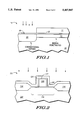
- FIGS. 2-5 illustrate process steps in accordance with one embodiment of the invention. Shown in FIG. 2, in cross section, is a portion of a semiconductor device 111 having already undergone some of the process steps in accordance with the invention.
- Device 111 includes an N-type semiconductor substrate region 112 which can be a uniformly doped continuous semiconductor body or a doped region of a semiconductor body such as an N-type well region, or an N-type tub, or the like. In the case of formation of a CMOS device, substrate region 112 will have an adjacent P-type region of similar construction (not shown).
- a field insulator 114 defines an active region 116 in substrate region 112.
- Preferably field insulator 114 is a thermally grown silicon oxide which is partially recessed into the silicon substrate and which, at least in part, extends above the original surface.
- a thin dielectric layer 118 overlies the active region 116 and a gate electrode 120 overlies dielectric layer 118 in a central portion of active region 116.
- Dielectric layer 118 is preferably silicon oxide thermally grown to a thickness of about 7.5 to 25 nanometers and gate electrode 120 is preferably formed from N-type polysilicon CVD deposited to a thickness of about 200 to 300 nanometers.
- a thermal oxidation process is carried out to form a silicon oxide layer 122 overlying gate electrode 120 and a layer 124 of semiconductor material is blanket deposited overlying gate electrode 120, dielectric layer 118 and field insulator 114.
- Layer 124 is preferably polysilicon CVD deposited to a thickness of about 150 nanometers.
- Layer 124 is doped with boron and fluorine atoms preferably by ion implantation of difluoroboron (BF 2 ) with a dose of about 10 15 to 10 16 ions per square centimeter and a implant energy of ranging from about 25 to 100 KeV.
- BF 2 difluoroboron
- a capping layer 126 is deposited overlying layer 124, as shown in FIG. 3.
- Capping layer 126 is formed from a diffusion barrier material such as silicon nitride deposited to a thickness sufficient to prevent the out-diffusion of boron atoms from layer 124.
- Capping layer 126 can also be formed by the deposition of an oxynitride material.
- the thermal annealing process diffuses boron atoms from layer 124 through dielectric layer 118 forming shallow PN junctions at a precise distance from the substrate surface.
- Those skilled in the art will appreciate that the optimum process conditions will be dependent upon the materials used and the desired characteristics of the shallow boron region formed in the substrate. For example, the annealing temperature and time will depend upon several factors including, the total boron dose delivered to the semiconductor material layer, the thickness of the semiconductor material layer and the thickness of the dielectric layer.
- capping layer 126 is removed by an isotropic etching process and layer 124 is anisotropically etched to from a sidewall spacer 132 on the edge of gate electrode 120, as shown in FIG. 4.
- Anisotropic etching is an etch process carried out in a reactive-ion-etch (PIE) reactor using a combination of etch gases, and reactor conditions, which result in more rapid etching of a material in the vertical direction than the horizontal direction.
- PIE reactive-ion-etch
- the directionality of the anisotropic RIE process applied to layer 124 results in the formation of sidewall spacer 132 having a substantially vertical edge.
- etch gases are such as chlorine and hydrogenated halogens are used which will react with the material of layer 124 much more rapidly than dielectric layer 118 underlying layer 124.
- active area 116 is implanted with boron atoms to form heavily doped P-type source and drain regions 134 and and 136.
- the boron implant is self-aligned to gate electrode 120 and diffused source and drain regions 128 and 130 by using sidewall spacer 132 as an implant mask.
- MOS transistor 138 is removed by an isotopic etch and device 111 is annealed at about 900 for about 15 minutes to form an MOS transistor 138, as illustrated in FIG. 5.
- the source of transistor 138 includes a heavily doped region 134 and a more lightly doped region 128.
- the drain of transistor 138 includes a heavily doped region 136 and a more lightly doped region 130.
- MOS transistor 138 exhibits improved operating performance compared to a transistor having a conventionally formed LDD structure.
- the lateral diffusion of boron into channel region 137 is reduced by the boron diffusion process used to form lightly doped regions 128 and 130.
- the reduced lateral diffusion results in fewer short channel effects such as drain induced barrier lowering (DIBL).
- DIBL drain induced barrier lowering
- GIDL gate-induced-drain-leakage
- the impurity concentration and distribution profile of the extrinsic base immediately adjacent to the emitter is established in a precise manner by diffusing the impurity through a dielectric layer formed on a portion of the active device surface.
- the extrinsic base region is self-aligned to the dielectric layer which, upon diffusion of impurities therethrough, produces a tapered base link between the extrinsic and intrinsic base regions.
- the base link formed in accordance with the invention provides a region having a precise electrical resistance and a shallow distribution profile which avoids excessive base impurity concentrations at the edge of the emitter region and spaces the extrinsic base region apart a predetermined distance from the intrinsic base region.
- FIGS. 6-10 illustrate schematically in cross section process steps in accordance with a second embodiment of the invention.
- a portion of a semiconductor device 211 formed in accordance with this embodiment is shown in FIG. 6.
- Device 211 includes a substrate 212 having an N-type well region 214 overlying an N-type buried layer 216.
- substrate 212 is comprised of an epitaxial layer overlying a single crystal silicon body. Buried layer 216 is formed by doping a portion of the single crystal silicon surface prior to forming the epitaxial layer.
- Device 211 further includes an isolation region 218 formed at the substrate surface and a collector contact 222 extending from the surface of substrate 212 to buried layer 216.
- collector contact 222 is spaced apart from well region 214 by an intermediate portion 224 of isolation region 218.
- Intermediate portion 224 defines an active surface 226 overlying well region 214.
- Collector contact 222 is conventionally formed by diffusing N-type impurity atoms into substrate 212.
- a screen layer 228, formed on active surface 226 overlies well region 214 and collector contact 222.
- Isolation region 218 provides electrical isolation to electrically isolate active surface 226 from adjacent devices.
- isolation region 218 is formed from a thick silicon oxide layer which is at least partially recessed into the substrate surface.
- Screen layer 228 can be any dielectric material through which semiconductor dopant impurity atoms can diffuse and which is differentially etchable with respect to a semiconductor material.
- screen layer 228 is silicon oxide formed on active surface 226 by thermal oxidation.
- screen layer 228 is patterned and etched to form a oxide pad 230 overlying a central portion of active surface 226, as illustrated in FIG. 7.
- the etch exposes a base contact region 232 in the periphery of active surface 226 adjacent to the edges of oxide pad 230.
- a layer 234 of semiconductor material, preferably polysilicon deposited by CVD, is formed overlying oxide pad 230 and base contact region 232.
- a photomask pattern 236 is formed on semiconductor layer 234 exposing a base contact portion of layer 234 and the exposed portion is doped with boron and fluorine atoms preferably by ion implantation of BF 2 with a dose of about 10 14 to 10 16 ions per square centimeter and a implant energy of about 40 to 80 KeV.
- a layer 237 of insulating material is deposited overlying layer 234.
- the insulating material is preferably silicon oxide deposited to a thickness of about two hundred to four hundred nanometers by means of CVD deposition using tetraethoxysilane (TEOS). Alternatively, thermally grown silicon oxide or an oxide-nitride composite layer or the like can be used. Insulation layer 237 and semiconductor layer 234 are photolithographically patterned and etched to form an insulated base electrode 238 illustrated in FIG. 8. Base electrode 238 overlies base contact region 232 and a peripheral portion of oxide pad 230.
- TEOS tetraethoxysilane
- a P-type intrinsic base region 240 is formed preferably by ion implantation of a P-type dopant, such as boron, into active well region 214 using base electrode 238 as an implant mask.
- a P-type dopant such as boron
- the outline of base electrode 238 on N-well region 214 is used as a doping mask for the formation of an intrinsic base region 240.
- Intrinsic base region 240 is thus self-aligned to base electrode 238 and forms the active base for the bipolar transistor under construction.
- the ion implantation step establishes a dopant concentration of about 5 ⁇ 10 17 to 5 ⁇ 10 18 atoms per cubic centimeter in intrinsic base region 240.
- device 211 is thermally annealed to diffuse boron atoms from base electrode 238 into well region 214 to form an extrinsic base region 242 and a diffused base link 244.
- base contact region 232 boron atoms diffuse directly from base electrode 238 directly into well region 214 forming a deeply diffused extrinsic base.
- Base link 244 is formed by boron atoms which diffuse through oxide pad 230 where the diffusion rate is limited by the flux of boron atoms through the oxide layer.
- the annealing process is carried out at a temperature of about about 800° to 1000° C. for about 5 to 60 minutes.
- Base link 244 is characterized by a high boron concentration at the substrate surface and a uniform shallow doping profile in the substrate.
- a sidewall spacer 246 is formed on base electrode 238 by first CVD depositing a layer of sidewall spacer forming material to a thickness of about one hundred to three hundred nanometers onto the base electrode, then, anisotropically etching the spacer forming material.
- the sidewall spacer material is a dielectric material differentially etchable to silicon oxide such as silicon nitride.
- the portion of oxide pad 230 exposed by sidewall spacer 246 is etched away leaving oxide portions underlying sidewall spacer 246 and a portion of base electrode 238.
- a selective oxide etching process is used to remove the exposed portion of oxide pad 230 and expose a portion of the surface of well region 214 between oxide portions 248 and 250.
- oxide pad 230 is RIE etched using fluorinated hydrocarbon etch gases to etch silicon oxide preferentially to the underlying substrate while avoiding damage to the substrate surface. During the etching of oxide pad 230, a portion of relatively thicker insulting layer 237 is also etched. The pad oxide etch process removes about 20 to 40 nanometers of material from the surface of insulating layer 237.
- an emitter structure is formed as illustrated in FIG. 10.
- a polysilicon layer is then CVD deposited to a thickness of about 100 to 300 nanometers and is doped with an N-type impurity, either during polysilicon deposition, or immediately after deposition.
- the polysilicon layer is anisotropically etched to form the emitter electrode 252 depicted in FIG. 10.
- the dopants previously introduced into the emitter are diffused into well region 214 to form an emitter region 254.
- Emitter region 254 is formed entirely within base intrinsic base region 240 and forms a PN junction therewith at a point in well region 214 directly beneath emitter electrode 252.
- the process then continues in a conventional manner to complete the fabrication of semiconductor device 211 including the formation of a collector electrode, passivation overcoat and metal contacts to interconnect the electrodes with other circuit elements. For the purpose of clearly illustrating the present embodiment these additional structures are not shown.
- Semiconductor device 211 formed in accordance with the invention, exhibits improved electrical performance by forming base link 244 intermediate to extrinsic base regions 242 and intrinsic base region 240.
- the boron diffused base link reduces hot carrier injection along the emitter periphery because a more gradual change of the dopant concentration in the emitter-base region is achieved.
- the extrinsic and intrinsic base regions can be formed in a single diffusion step.
- the BF 2 doping step illustrated in FIG. 7 is performed and resist pattern 236 is removed.
- insulating layer 237 is deposited onto semiconductor layer 234 to form an insulation cap over semiconductor layer 234.
- An anneal, in the presence of hydrogen gas, is performed to diffuse the boron in semiconductor layer 234 into substrate 212 forming both intrinsic base region 240 and extrinsic base region 242 in a single diffusion step.
- the resulting doping structure is illustrated in FIG. 11.
- a shallow intrinsic base region having a high surface doping concentration is formed by diffusion of boron atoms through oxide pad 230. Following the boron diffusion step, processing is performed in an identical manner to that previously described and illustrated in FIGS. 9 and 10.
- a 7.5 nanometer gate oxide was thermally grown on the substrate surface.
- a first polysilicon layer was CVD deposited to a thickness of 250 nanometers onto the gate oxide.
- a pattern was defined on the polysilicon and the polysilicon was anisotropically etched to form a gate electrode structure.
- the photoresist pattern was removed and an oxide layer was formed on the gate electrode by thermal oxidation.
- a second polysilicon layer was deposited to a thickness of 150 nanometers onto the substrate and the gate electrode.
- the second polysilicon layer was doped by ion implantation of BF 2 with a dose of 1 ⁇ 10 16 ions per square centimeter.
- a low temperature oxide (LTO) layer was deposited followed by the low temperature deposition of a silicon nitride layer.
- An anneal step was performed for 45 minutes at 900° C. to diffuse the boron from the second polysilicon layer, through the gate oxide and into the substrate.
- the silicon nitride layer and the LTO layer were removed and the second polysilicon layer anisotropically etched to form a sidewall spacer on the gate electrode.
- heavily doped P+ source and drain regions were formed in the substrate by ion implantation of boron with a dose of 5 ⁇ 10 15 ions per square centimeter.
- the substrate was annealed for 15 minutes at 900° C.
- a passivation layer was deposited and metal contacts were formed in a conventional manner to complete the device fabrication.
- FIG. 12 Shown in FIG. 12, is a plot of the effective channel length (in microns) versus the physical gate electrode length (in microns) for devices fabricated using conventional processes (labeled “P+ only” and “conventional LDD” respectively) and the structure formed according to the above example (labeled "boron penetrated LDD").
- the boron penetrated structure has a larger effective channel length for a given physical gate length than corresponding devices of the prior art. This result indicates the device formed in accordance with the invention is effectively preventing the electrical field of the heavily doped P+ regions from overlapping onto the gate region.
- FIG. 13 Shown in FIG. 13, is a plot of the log of drain current (in amps) versus drain voltage (in volts) at 0 applied gate voltage for devices of the prior art (labeled “P+ only” and “conventional LDD” respectively) and the structure formed according to the above example (labeled "boron penetrated LDD").
- the results shown in the plot indicate an increased drain breakdown voltage is achieved compared to devices of the prior art. This increase is believed to be brought about through a reduction in the gate induced drain barrier lowering achieved by the shallow boron LDD region formed in accordance with the invention.
Abstract
A method is provided for the formation of ultra-shallow boron doped regions in a semiconductor device. In one embodiment of the invention an N-type semiconductor substrate (15) is provided having a first P-type region formed therein. A dielectric layer (16) is formed on the substrate surface and a material layer (17) doped with fluorinated boron is formed on the dielectric layer (16). A second P-type region (22), characterized by a high dopant concentration at the substrate surface and a uniform junction profile, is formed in the substrate adjacent to the first P-type region by diffusing boron atoms from the material layer (17) through the dielectric layer (16) and into the substrate (15). The second P-type region (22) has a very shallow junction depth which is closer to the substrate surface than the first P-type region.
Description
This is a division of application Ser. No. 07/695,119, filed May 3, 1991, now U.S. Pat. No. 5,279,976.
This invention relates in general to a method for fabricating a semiconductor device, and more particularly to a method for fabricating a VLSI semiconductor device incorporating shallow doped regions having a high dopant concentration at the surface.
The semiconductor industry is characterized by a trend toward fabricating larger and more complex circuits on a given semiconductor chip. The larger and more complex circuits are achieved by reducing the size of individual devices within the circuits and spacing the devices closer together. As the dimensions of the individual components within a device such as an MOS or bipolar transistor are reduced and the device components brought closer together, improved electrical performance can be obtained. However, attention must be given to the formation of doped regions in the substrate to insure that deleterious electrical field conditions do not arise.
As the size of device components such as the transistor gate in an MOS device and the emitter region in a bipolar device, are reduced, the junction depth of doped regions formed in the semiconductor substrate must also be reduced. The formation of shallow junctions having a uniform doping profile and a high surface concentration has proven to be very difficult. A commonly used technique is to implant dopant atoms into the substrate with an ion implantation apparatus. Using ion implantation, the high energy dopant atoms bombard the surface of the substrate at high velocity and are driven into the substrate. While this method has proven effective for the formation of doped regions having moderately deep junctions, the formation of ultra-shallow junctions using ion implantation is extremely difficult. Both the path of the energized dopant atoms within the substrate and the implant uniformity are difficult to control at the low energies necessary to form shallow implanted junctions. The implantation of energized dopant atoms damages the crystal lattice in the substrate which is difficult to repair. Dislocations resulting from the lattice damage can easily spike across a shallow junction giving rise to current leakage across the junction. Moreover, the implantation of P-type dopants such as boron, which diffuse rapidly in silicon, results in excessive dispersion of dopant atoms after they are introduced into the substrate. It then becomes difficult to form a highly confined concentration of P-type dopant atoms in a specified area in the substrate and especially at the surface of the substrate.
A similar problem is encountered when a dopant such as boron is diffused from an overlying polysilicon layer directly into a silicon substrate. The boron rapidly diffuses through the polysilicon and into the substrate. The rapid introduction of boron atoms into the substrate, coupled with the high diffusivity of boron in silicon, results in excessive lateral diffusion.
The most serious consequence of the excessive dopant diffusivity is termed "lateral diffusion" wherein a diffused region extending laterally parallel with the surface of the substrate is formed. If the lateral diffusion becomes too great, the device performance will be severely degraded and in the worst case, total functional failure occurs. In P-channel MOS transistors and NPN vertical bipolar transistors, the active components which substantially determine performance factors such as current gain and switching speed are fabricated by forming shallow boron doped regions in the substrate. For example, the boron doped LDD portion of the MOS P-channel transistor must offset the drain electric field from the channel region to prevent hot carrier injection while simultaneously carrying a large quantity of charge to maintain a high current gain. In the vertical NPN bipolar transistor, the boron doped base region must have a high dopant concentration to maintain high current gain but not excessively overlap the emitter region. Excessive lateral diffusion of the base regions can result in a low emitter-base breakdown voltage and hot carrier injection along the periphery of the emitter.
In VLSI device fabrication, as dimensions become smaller, lateral dopant diffusion, especially P-type dopant diffusion, must be minimized in order to fully realize enhanced device performance. This is necessary to prevent the associated electric fields of the doped regions from overlapping and forming unwanted parasitic capacitors within the device.
In practicing the present invention there is provided a method of fabricating a semiconductor device having shallow boron doped regions formed in a semiconductor substrate. The boron doped regions are characterized by a shallow junction depth and a high dopant surface concentration. In one embodiment, an N-type semiconductor substrate is provided and a dielectric layer is formed on the substrate surface. A material layer having a fluorinated-boron component is formed overlying the dielectric layer. A first P-type impurity region having a first selected junction depth is formed in the substrate. Boron atoms are diffused in the presence of hydrogen from the fluorinated material layer through the dielectric layer and into the substrate. The boron diffusion forms a second P-type impurity region having a high surface concentration adjacent to the first P-type region. The second P-type region has a PN junction which is closer to the surface of the substrate than the PN junction of the first P-type region. The second P-type region is further characterized by a high dopant concentration at the substrate surface and a uniform junction profile in the substrate.
FIG. 1, illustrates, in cross section, a doped region of a semiconductor device formed in accordance with the invention in comparison with a conventionally formed doped region;
FIGS. 2-5 illustrate, in cross section, process steps in accordance with one embodiment of the invention;
FIGS. 6-10 illustrate, in cross section, process steps in accordance with another embodiment of the invention;
FIG. 11 illustrates, in cross section, a semiconductor device formed in accordance with yet another embodiment of the invention;
FIG. 12 is a plot of effective channel length versus physical gate length for a device formed in accordance with the invention versus devices of the prior art; and
FIG. 13 is a plot of log drain current versus drain voltage for a device formed in accordance with the invention versus devices of the prior art.
It will be appreciated that for simplicity and clarity of illustration elements shown in the FIGURES have not necessarily been drawn to scale. For example, the dimensions of some of the elements are exaggerated relative to each other for clarity. Further, where considered appropriate, reference numerals have been repeated among the FIGURES to indicate corresponding elements.
It has been discovered that boron can be diffused in the presence of hydrogen from a fluorinated semiconductor material through an underlying dielectric layer and into an N-type semiconductor substrate to form a shallow diffused region in the substrate. The diffusion process forms a P-type region having a high boron concentration at the substrate surface. It has further been discovered that a PN junction created by the boron diffusion can, under a specified set of process conditions, be reproducibly formed at a precise depth in the substrate. The ability to repeatably form a shallow P-type region having a smooth PN junction profile and having a high impurity concentration at the substrate surface offers performance advantages in both MOS and bipolar transistor device applications. The process of the present invention will be described in terms of a general embodiment to be followed by specific process embodiments thereof.
Illustrated in FIG. 1, in cross section, is a portion of a semiconductor device 14 including an N-type substrate 15 having a dielectric layer 16 overlying a portion of the substrate surface. Dielectric layer 16 has a thickness ranging from about 7.5 to 17.5 nanometers and can be formed by thermally oxidizing the surface of substrate 15. Alternatively dielectric layer 16 can be formed by chemical vapor deposition (CVD), RF sputtering, molecular beam deposition and the like. A layer 17 of semiconductor material overlies a portion of dielectric layer 16 leaving a portion 18 of the substrate surface covered only by dielectric layer 16. Layer 17 has as a constituent a fluorinated-boron component distributed throughout the body of the structure shown in FIG. 1. Layer 17 can be any semiconducting material capable of incorporating a fluorinated-boron component and releasing boron upon exposure to thermal radiation. Preferably, layer 17 is polysilicon impregnated with flourine atoms and boron atoms. Excess flourine is present in a ratio of about two flourine atoms to one boron atom however, this ratio can vary depending upon the specific process conditions used. For example, the fluorine and boron atoms can be introduced into layer 17 by molecular deposition, ion implantation, CVD and the like during film formation. In a preferred embodiment, difluoroboron is ion implanted into layer 17 with a dose of about 1015 to 1016 ions per square centimeter which, after annealing, yields a total boron surface concentration in the range of about 1017 to 1020 atoms per cubic centimeter. Once layer 17 has been formed having a fluorinated boron component, a photolithographic patterning process is used followed by anisotropic etching to form the configuration shown in FIG. 1.
The structure illustrated in FIG. 1 further includes an ion implanted region 20 which is formed by ion implantation of boron ions through dielectric layer 16 and into substrate 15. The implant dose and energy is adjusted to produce as shallow boron distribution profile as possible while maintaining a high surface concentration of boron atoms. The junction formed in the substrate by the ion implantation process is labeled "conventional doping" in FIG. 1. After the formation of implanted region 20, device 14 is subjected to a thermal annealing process to repair crystal damage caused by the implanted atoms and to diffuse boron atoms from layer 17 into substrate 15. The thermal anneal can be carried out in a conventional convection furnace or by a radiative process such as rapid thermal annealing. The diffusion process forms a P-type impurity region 22 in substrate 15. The PN junction formed by the boron diffusion into the N-type substrate, labeled "boron penetrated", occurs at a uniform shallow distance from the substrate surface. The distance of the PN junction from the substrate surface, or in other words, the junction depth, is dependent upon by the diffusion rate of boron atoms through the dielectric material. The deeply channeled implanted region 20 is characteristic of the formation of boron regions using a conventional ion implant process and can be directly compared with the uniform shallow junction formed by the process of the present invention.
FIGS. 2-5 illustrate process steps in accordance with one embodiment of the invention. Shown in FIG. 2, in cross section, is a portion of a semiconductor device 111 having already undergone some of the process steps in accordance with the invention. Device 111 includes an N-type semiconductor substrate region 112 which can be a uniformly doped continuous semiconductor body or a doped region of a semiconductor body such as an N-type well region, or an N-type tub, or the like. In the case of formation of a CMOS device, substrate region 112 will have an adjacent P-type region of similar construction (not shown). A field insulator 114 defines an active region 116 in substrate region 112. Preferably field insulator 114 is a thermally grown silicon oxide which is partially recessed into the silicon substrate and which, at least in part, extends above the original surface. A thin dielectric layer 118 overlies the active region 116 and a gate electrode 120 overlies dielectric layer 118 in a central portion of active region 116. Dielectric layer 118 is preferably silicon oxide thermally grown to a thickness of about 7.5 to 25 nanometers and gate electrode 120 is preferably formed from N-type polysilicon CVD deposited to a thickness of about 200 to 300 nanometers. A thermal oxidation process is carried out to form a silicon oxide layer 122 overlying gate electrode 120 and a layer 124 of semiconductor material is blanket deposited overlying gate electrode 120, dielectric layer 118 and field insulator 114. Layer 124 is preferably polysilicon CVD deposited to a thickness of about 150 nanometers. Layer 124 is doped with boron and fluorine atoms preferably by ion implantation of difluoroboron (BF2) with a dose of about 1015 to 1016 ions per square centimeter and a implant energy of ranging from about 25 to 100 KeV.
After the formation and doping of layer 124, a capping layer 126 is deposited overlying layer 124, as shown in FIG. 3. Capping layer 126 is formed from a diffusion barrier material such as silicon nitride deposited to a thickness sufficient to prevent the out-diffusion of boron atoms from layer 124. Capping layer 126 can also be formed by the deposition of an oxynitride material. Once capping layer 126 is formed, device 111 is thermally annealed at a temperature of about 800° to 1000° C. for about 5 to 60 minutes to form shallow P-type diffused source and drain regions 128 and 130 in active region 116. The thermal annealing process diffuses boron atoms from layer 124 through dielectric layer 118 forming shallow PN junctions at a precise distance from the substrate surface. Those skilled in the art will appreciate that the optimum process conditions will be dependent upon the materials used and the desired characteristics of the shallow boron region formed in the substrate. For example, the annealing temperature and time will depend upon several factors including, the total boron dose delivered to the semiconductor material layer, the thickness of the semiconductor material layer and the thickness of the dielectric layer.
Following the formation of P-type diffused regions 128 and 130, capping layer 126 is removed by an isotropic etching process and layer 124 is anisotropically etched to from a sidewall spacer 132 on the edge of gate electrode 120, as shown in FIG. 4. Anisotropic etching is an etch process carried out in a reactive-ion-etch (PIE) reactor using a combination of etch gases, and reactor conditions, which result in more rapid etching of a material in the vertical direction than the horizontal direction. The directionality of the anisotropic RIE process applied to layer 124 results in the formation of sidewall spacer 132 having a substantially vertical edge. Additionally, etch gases are such as chlorine and hydrogenated halogens are used which will react with the material of layer 124 much more rapidly than dielectric layer 118 underlying layer 124. Once sidewall spacer 132 is formed, active area 116 is implanted with boron atoms to form heavily doped P-type source and drain regions 134 and and 136. The boron implant is self-aligned to gate electrode 120 and diffused source and drain regions 128 and 130 by using sidewall spacer 132 as an implant mask.
The source and drain structures illustrated, with a heavily doped region and a lightly doped region are representative of the well known LDD structure. A channel region 137 separates the source and drain regions. As a result of the fabrication process in accordance with the invention, MOS transistor 138 exhibits improved operating performance compared to a transistor having a conventionally formed LDD structure. For example, the lateral diffusion of boron into channel region 137 is reduced by the boron diffusion process used to form lightly doped regions 128 and 130. The reduced lateral diffusion results in fewer short channel effects such as drain induced barrier lowering (DIBL). Additionally, adverse effects from gate-induced-drain-leakage (GIDL) are reduced because the high surface concentration region, obtained by controlled boron diffusion through dielectric layer 118, minimizes lateral band bending of the oxide/silicon interface near the gate edge. Furthermore, the drain breakdown voltage is increased because the boron diffusion process provides a high boron surface concentration in lightly doped regions 128 and 130. Further description of the foregoing advantages of the invention and comparative results are hereinafter provided in an example illustrative of the invention.
To obtain optimum performance in vertical bipolar transistor fabricated to VLSI dimensions, attention must be given to the impurity concentrations and profile in the intrinsic base region and in the extrinsic base region near the edges of the diffused emitter. Excessive overlap of the highly doped extrinsic base region around the emitter lowers the emitter-base breakdown voltage and increases hot-carrier injection along the emitter periphery. Conversely, if the impurity concentration in the extrinsic base region adjacent to the emitter is too low the base resistance will be large and lateral punch-through of charge carriers between the emitter and the collector can occur. In the present embodiment, the impurity concentration and distribution profile of the extrinsic base immediately adjacent to the emitter is established in a precise manner by diffusing the impurity through a dielectric layer formed on a portion of the active device surface. The extrinsic base region is self-aligned to the dielectric layer which, upon diffusion of impurities therethrough, produces a tapered base link between the extrinsic and intrinsic base regions.
The base link formed in accordance with the invention provides a region having a precise electrical resistance and a shallow distribution profile which avoids excessive base impurity concentrations at the edge of the emitter region and spaces the extrinsic base region apart a predetermined distance from the intrinsic base region.
FIGS. 6-10 illustrate schematically in cross section process steps in accordance with a second embodiment of the invention. A portion of a semiconductor device 211 formed in accordance with this embodiment is shown in FIG. 6. Device 211 includes a substrate 212 having an N-type well region 214 overlying an N-type buried layer 216. Typically, substrate 212 is comprised of an epitaxial layer overlying a single crystal silicon body. Buried layer 216 is formed by doping a portion of the single crystal silicon surface prior to forming the epitaxial layer.
In accordance with the invention, screen layer 228 is patterned and etched to form a oxide pad 230 overlying a central portion of active surface 226, as illustrated in FIG. 7. The etch exposes a base contact region 232 in the periphery of active surface 226 adjacent to the edges of oxide pad 230. A layer 234 of semiconductor material, preferably polysilicon deposited by CVD, is formed overlying oxide pad 230 and base contact region 232. Next, a photomask pattern 236 is formed on semiconductor layer 234 exposing a base contact portion of layer 234 and the exposed portion is doped with boron and fluorine atoms preferably by ion implantation of BF2 with a dose of about 1014 to 1016 ions per square centimeter and a implant energy of about 40 to 80 KeV.
After doping semiconductor layer 234, photomask pattern 236 is removed and a layer 237 of insulating material is deposited overlying layer 234. The insulating material is preferably silicon oxide deposited to a thickness of about two hundred to four hundred nanometers by means of CVD deposition using tetraethoxysilane (TEOS). Alternatively, thermally grown silicon oxide or an oxide-nitride composite layer or the like can be used. Insulation layer 237 and semiconductor layer 234 are photolithographically patterned and etched to form an insulated base electrode 238 illustrated in FIG. 8. Base electrode 238 overlies base contact region 232 and a peripheral portion of oxide pad 230. A P-type intrinsic base region 240 is formed preferably by ion implantation of a P-type dopant, such as boron, into active well region 214 using base electrode 238 as an implant mask. The outline of base electrode 238 on N-well region 214 is used as a doping mask for the formation of an intrinsic base region 240. Intrinsic base region 240 is thus self-aligned to base electrode 238 and forms the active base for the bipolar transistor under construction. The ion implantation step establishes a dopant concentration of about 5×10¹⁷ to 5×10¹⁸ atoms per cubic centimeter in intrinsic base region 240.
The process is continued as illustrated in FIG. 9. Following the formation of intrinsic base region 240, device 211 is thermally annealed to diffuse boron atoms from base electrode 238 into well region 214 to form an extrinsic base region 242 and a diffused base link 244. In base contact region 232, boron atoms diffuse directly from base electrode 238 directly into well region 214 forming a deeply diffused extrinsic base. Base link 244 is formed by boron atoms which diffuse through oxide pad 230 where the diffusion rate is limited by the flux of boron atoms through the oxide layer. The annealing process is carried out at a temperature of about about 800° to 1000° C. for about 5 to 60 minutes. Base link 244 is characterized by a high boron concentration at the substrate surface and a uniform shallow doping profile in the substrate.
Following the annealing step, a sidewall spacer 246 is formed on base electrode 238 by first CVD depositing a layer of sidewall spacer forming material to a thickness of about one hundred to three hundred nanometers onto the base electrode, then, anisotropically etching the spacer forming material. Preferably, the sidewall spacer material is a dielectric material differentially etchable to silicon oxide such as silicon nitride. The portion of oxide pad 230 exposed by sidewall spacer 246 is etched away leaving oxide portions underlying sidewall spacer 246 and a portion of base electrode 238. A selective oxide etching process is used to remove the exposed portion of oxide pad 230 and expose a portion of the surface of well region 214 between oxide portions 248 and 250. In a preferred method, oxide pad 230 is RIE etched using fluorinated hydrocarbon etch gases to etch silicon oxide preferentially to the underlying substrate while avoiding damage to the substrate surface. During the etching of oxide pad 230, a portion of relatively thicker insulting layer 237 is also etched. The pad oxide etch process removes about 20 to 40 nanometers of material from the surface of insulating layer 237.
Once a contact opening has been made exposing a portion of the surface of well region 214, an emitter structure is formed as illustrated in FIG. 10. A polysilicon layer is then CVD deposited to a thickness of about 100 to 300 nanometers and is doped with an N-type impurity, either during polysilicon deposition, or immediately after deposition. Next, the polysilicon layer is anisotropically etched to form the emitter electrode 252 depicted in FIG. 10. The dopants previously introduced into the emitter are diffused into well region 214 to form an emitter region 254. Emitter region 254 is formed entirely within base intrinsic base region 240 and forms a PN junction therewith at a point in well region 214 directly beneath emitter electrode 252.
The process then continues in a conventional manner to complete the fabrication of semiconductor device 211 including the formation of a collector electrode, passivation overcoat and metal contacts to interconnect the electrodes with other circuit elements. For the purpose of clearly illustrating the present embodiment these additional structures are not shown.
Alternatively, as may be desirable because of the particular electrical requirements of the semiconductor device under construction, the extrinsic and intrinsic base regions can be formed in a single diffusion step. To form the extrinsic and intrinsic base regions in a single step, the BF2 doping step illustrated in FIG. 7 is performed and resist pattern 236 is removed. As previously described, insulating layer 237 is deposited onto semiconductor layer 234 to form an insulation cap over semiconductor layer 234. An anneal, in the presence of hydrogen gas, is performed to diffuse the boron in semiconductor layer 234 into substrate 212 forming both intrinsic base region 240 and extrinsic base region 242 in a single diffusion step. The resulting doping structure is illustrated in FIG. 11. A shallow intrinsic base region having a high surface doping concentration is formed by diffusion of boron atoms through oxide pad 230. Following the boron diffusion step, processing is performed in an identical manner to that previously described and illustrated in FIGS. 9 and 10.
Without further elaboration, it is believed that one skilled in the art can, using the preceding description, utilize the invention to its fullest extent. The following example is, therefore, to be construed as merely illustrative, and not limitative of the remainder of the disclosure in any way whatsoever.
Beginning with an N-type silicon substrate having a surface concentration of about 1017 atoms per cubic centimeter, a 7.5 nanometer gate oxide was thermally grown on the substrate surface. A first polysilicon layer was CVD deposited to a thickness of 250 nanometers onto the gate oxide. Using conventional photolithography, a pattern was defined on the polysilicon and the polysilicon was anisotropically etched to form a gate electrode structure. The photoresist pattern was removed and an oxide layer was formed on the gate electrode by thermal oxidation. A second polysilicon layer was deposited to a thickness of 150 nanometers onto the substrate and the gate electrode. The second polysilicon layer was doped by ion implantation of BF2 with a dose of 1×10¹⁶ ions per square centimeter. After implanting the polysilicon layer, a low temperature oxide (LTO) layer was deposited followed by the low temperature deposition of a silicon nitride layer. An anneal step was performed for 45 minutes at 900° C. to diffuse the boron from the second polysilicon layer, through the gate oxide and into the substrate. The silicon nitride layer and the LTO layer were removed and the second polysilicon layer anisotropically etched to form a sidewall spacer on the gate electrode. Then, heavily doped P+ source and drain regions were formed in the substrate by ion implantation of boron with a dose of 5×10¹⁵ ions per square centimeter. After performing the P+ implant, the substrate was annealed for 15 minutes at 900° C. A passivation layer was deposited and metal contacts were formed in a conventional manner to complete the device fabrication.
Shown in FIG. 12, is a plot of the effective channel length (in microns) versus the physical gate electrode length (in microns) for devices fabricated using conventional processes (labeled "P+ only" and "conventional LDD" respectively) and the structure formed according to the above example (labeled "boron penetrated LDD"). As can be observed in the plot, the boron penetrated structure has a larger effective channel length for a given physical gate length than corresponding devices of the prior art. This result indicates the device formed in accordance with the invention is effectively preventing the electrical field of the heavily doped P+ regions from overlapping onto the gate region.
Shown in FIG. 13, is a plot of the log of drain current (in amps) versus drain voltage (in volts) at 0 applied gate voltage for devices of the prior art (labeled "P+ only" and "conventional LDD" respectively) and the structure formed according to the above example (labeled "boron penetrated LDD"). The results shown in the plot indicate an increased drain breakdown voltage is achieved compared to devices of the prior art. This increase is believed to be brought about through a reduction in the gate induced drain barrier lowering achieved by the shallow boron LDD region formed in accordance with the invention.
Thus it is apparent that there has been provided, in accordance with the invention, a method for forming a semiconductor device having a shallow doped region which fully meets the advantages set forth above. Although the invention has been described and illustrated with reference to specific illustrative embodiments thereof, it is not intended that the invention be limited to those illustrative embodiments. Those skilled in the art will recognize that variations and modifications can be made without departing from the spirit of the invention. For example, discrete components such as diodes can be fabricated with diffused structures formed by boron penetration. Furthermore, MOS devices and bipolar devices can be simultaneously fabricated in accordance with the invention on the same semiconductor substrate to produce BiCMOS devices. It is therefore intended to include within the invention all such variations and modifications as fall within the scope of the appended claims and equivalents thereof.
Claims (8)
1. A method for fabricating a semiconductor device comprising:
providing an N-type semiconductor substrate having a gate electrode overlying a gate dielectric layer;
forming a material layer having a fluorinated-boron component overlying the gate electrode and the gate dielectric layer;
diffusing boron atoms from the material layer through the dielectric layer and into the substrate in the presence of hydrogen to form lightly doped regions having a first junction depth in the substrate adjacent to the gate electrode, the lightly doped regions being characterized by a high concentration of boron atoms at the substrate surface and a uniform shallow doping profile in the substrate;
etching the material layer to form sidewall spacers adjacent the gate electrode; and
forming a heavily doped region in the substrate having a second junction depth using the sidewall spacers as a dopant mask wherein the second junction depth is farther removed from the substrate surface than the first junction depth.
2. The method of claim 1 wherein the step of forming a material layer comprises depositing a layer of polysilicon onto the gate electrode and implanting BF2 ions into the polysilicon layer.
3. The method of claim 1 wherein the step of diffusing comprises thermally annealing at a temperature of 800° to 1000° C. for 5 to 60 minutes.
4. The method of claim 1 wherein the step of providing a gate dielectric layer comprises thermally oxidizing the semiconductor substrate to form an oxide layer having a thickness of 5 to 15 nanometers.
5. A method for fabricating a semiconductor device comprising:
providing a semiconductor substrate having a gate dielectric layer thereon;
depositing a first polysilicon layer overlying the gate dielectric layer;
photolithographically patterning and etching the polysilicon layer to form a gate electrode;
oxidizing the gate electrode to form an oxide layer thereon;
depositing a second polysilicon layer overlying the gate electrode;
implanting BF2 ions into the second polysilicon layer;
depositing an insulating layer overlying the second polysilicon layer;
diffusing boron atoms from the second polysilicon layer through the gate dielectric layer and into the substrate to form lightly doped P-type source and drain regions having a first junction depth, the lightly doped regions being characterized by a high concentration of boron atoms at the substrate surface and a uniform shallow doping profile in the substrate;
etching the second polysilicon layer to form sidewall spacers on the gate electrode; and
implanting dopant atoms into the substrate to form heavily doped source and drain regions adjacent to the lightly doped source and drain regions having a second junction depth wherein the second junction depth is farther removed from the substrate surface than the first junction depth.
6. The method of claim 5 wherein the step of implanting BF2 ions comprises implanting a dose of 1×10¹⁶ ions per square centimeter.
7. The method of claim 5 wherein the step of diffusing boron atoms comprises thermally annealing at a temperature of 800° to 1000° C. for 5 to 60 minutes.
8. The method of claim 5 wherein the step of providing a gate dielectric layer comprises thermally oxidizing the semiconductor substrate to form an oxide layer having a thickness of 5 to 15 nanometers.
Priority Applications (1)
| Application Number | Priority Date | Filing Date | Title |
|---|---|---|---|
| US08/124,181 US5407847A (en) | 1991-05-03 | 1993-09-20 | Method for fabricating a semiconductor device having a shallow doped region |
Applications Claiming Priority (2)
| Application Number | Priority Date | Filing Date | Title |
|---|---|---|---|
| US07/695,119 US5279976A (en) | 1991-05-03 | 1991-05-03 | Method for fabricating a semiconductor device having a shallow doped region |
| US08/124,181 US5407847A (en) | 1991-05-03 | 1993-09-20 | Method for fabricating a semiconductor device having a shallow doped region |
Related Parent Applications (1)
| Application Number | Title | Priority Date | Filing Date |
|---|---|---|---|
| US07/695,119 Division US5279976A (en) | 1991-05-03 | 1991-05-03 | Method for fabricating a semiconductor device having a shallow doped region |
Publications (1)
| Publication Number | Publication Date |
|---|---|
| US5407847A true US5407847A (en) | 1995-04-18 |
Family
ID=24791654
Family Applications (2)
| Application Number | Title | Priority Date | Filing Date |
|---|---|---|---|
| US07/695,119 Expired - Fee Related US5279976A (en) | 1991-05-03 | 1991-05-03 | Method for fabricating a semiconductor device having a shallow doped region |
| US08/124,181 Expired - Fee Related US5407847A (en) | 1991-05-03 | 1993-09-20 | Method for fabricating a semiconductor device having a shallow doped region |
Family Applications Before (1)
| Application Number | Title | Priority Date | Filing Date |
|---|---|---|---|
| US07/695,119 Expired - Fee Related US5279976A (en) | 1991-05-03 | 1991-05-03 | Method for fabricating a semiconductor device having a shallow doped region |
Country Status (1)
| Country | Link |
|---|---|
| US (2) | US5279976A (en) |
Cited By (37)
| Publication number | Priority date | Publication date | Assignee | Title |
|---|---|---|---|---|
| US5593905A (en) * | 1995-02-23 | 1997-01-14 | Texas Instruments Incorporated | Method of forming stacked barrier-diffusion source and etch stop for double polysilicon BJT with patterned base link |
| US5643810A (en) * | 1995-10-06 | 1997-07-01 | Samsung Electronics Co., Ltd. | Methods of forming BiCMOS semiconductor devices |
| US5691212A (en) * | 1996-09-27 | 1997-11-25 | Taiwan Semiconductor Manufacturing Company, Ltd. | MOS device structure and integration method |
| US5707896A (en) * | 1996-09-16 | 1998-01-13 | Taiwan Semiconductor Manuacturing Company, Ltd. | Method for preventing delamination of interlevel dielectric layer over FET P+ doped polysilicon gate electrodes on semiconductor integrated circuits |
| WO1998013861A1 (en) * | 1996-09-24 | 1998-04-02 | Intel Corporation | Screening oxide for source and drain regions formed from solid dopant source |
| US5804476A (en) * | 1995-11-30 | 1998-09-08 | Samsung Electronics Co., Ltd. | Method of forming BiCMOS devices having mosfet and bipolar sections therein |
| US5811343A (en) * | 1996-07-15 | 1998-09-22 | Taiwan Semiconductor Manufacturing Company, Ltd. | Oxidation method for removing fluorine gas inside polysilicon during semiconductor manufacturing to prevent delamination of subsequent layer induced by fluorine outgassing dielectric |
| US5872047A (en) * | 1996-06-24 | 1999-02-16 | Hyundai Electronics Industries Co., Ltd. | Method for forming shallow junction of a semiconductor device |
| WO1999017351A1 (en) * | 1997-09-30 | 1999-04-08 | Infineon Technologies Ag | Reduction of gate-induced drain leakage in semiconductor devices |
| US5899747A (en) * | 1997-01-27 | 1999-05-04 | Vanguard International Semiconductor Corporation | Method for forming a tapered spacer |
| US5913123A (en) * | 1996-08-26 | 1999-06-15 | National Science Council | Manufacturing method for deep-submicron P-type metal-oxide semiconductor shallow junction |
| US5946581A (en) * | 1997-01-08 | 1999-08-31 | Advanced Micro Devices | Method of manufacturing a semiconductor device by doping an active region after formation of a relatively thick oxide layer |
| US5998273A (en) * | 1999-01-25 | 1999-12-07 | International Business Machines Corporation | Fabrication of semiconductor device having shallow junctions |
| US5998248A (en) * | 1999-01-25 | 1999-12-07 | International Business Machines Corporation | Fabrication of semiconductor device having shallow junctions with tapered spacer in isolation region |
| US6022771A (en) * | 1999-01-25 | 2000-02-08 | International Business Machines Corporation | Fabrication of semiconductor device having shallow junctions and sidewall spacers creating taper-shaped isolation where the source and drain regions meet the gate regions |
| US6025242A (en) * | 1999-01-25 | 2000-02-15 | International Business Machines Corporation | Fabrication of semiconductor device having shallow junctions including an insulating spacer by thermal oxidation creating taper-shaped isolation |
| US6051850A (en) * | 1995-12-30 | 2000-04-18 | Fairchild Korea Semiconductor Ltd. | Insulated gate bipolar junction transistors having built-in freewheeling diodes therein |
| US6235601B1 (en) * | 1995-12-28 | 2001-05-22 | Philips Electronics North America Corporation | Method of manufacturing a self-aligned vertical bipolar transistor |
| US6274465B1 (en) | 2000-03-30 | 2001-08-14 | International Business Machines Corporataion | DC electric field assisted anneal |
| US6287956B2 (en) * | 1997-04-25 | 2001-09-11 | Nec Corporation | Multilevel interconnecting structure in semiconductor device and method of forming the same |
| US6365472B1 (en) * | 1996-12-17 | 2002-04-02 | Kabushiki Kaisha Toshiba | Semiconductor device and method of manufacturing the same |
| US20030082922A1 (en) * | 2001-10-29 | 2003-05-01 | Seong-Jae Lee | Method of fabricating integrated circuit having shallow junction |
| US6620668B2 (en) | 2001-11-22 | 2003-09-16 | Electronics And Telecommunications Research Institute | Method of fabricating MOS transistor having shallow source/drain junction regions |
| US6642134B2 (en) * | 1999-09-22 | 2003-11-04 | Advanced Micro Devices, Inc. | Semiconductor processing employing a semiconductor spacer |
| US20040099895A1 (en) * | 2002-11-25 | 2004-05-27 | International Business Machines Corporation | High performance vertical PNP transistor and method |
| US6822311B2 (en) | 2000-03-30 | 2004-11-23 | International Business Machines Corporation | DC or AC electric field assisted anneal |
| US20050118770A1 (en) * | 2003-10-01 | 2005-06-02 | Texas Instruments, Inc. | Method for introducing hydrogen into a channel region of a metal oxide semiconductor (MOS) device |
| US20070212840A1 (en) * | 2006-03-07 | 2007-09-13 | Miller Gayle W Jr | Method for forming a self-aligned twin well region with simplified processing |
| CN100466205C (en) * | 2004-06-22 | 2009-03-04 | 东部亚南半导体株式会社 | Semiconductor devices and methods of manufacturing the same |
| US20100068876A1 (en) * | 2008-09-12 | 2010-03-18 | Taiwan Semiconductor Manufacturing Company, Ltd. | Methods of fabricating high-k metal gate devices |
| US20110269287A1 (en) * | 2010-04-28 | 2011-11-03 | Taiwan Semiconductor Manufacturing Company, Ltd. | Methods for doping fin field-effect transistors |
| US20120299121A1 (en) * | 2011-05-24 | 2012-11-29 | Taiwan Semiconductor Manufacturing Company., Ltd. | Source/Drain Formation and Structure |
| US8569158B2 (en) | 2011-03-31 | 2013-10-29 | Tokyo Electron Limited | Method for forming ultra-shallow doping regions by solid phase diffusion |
| US8580664B2 (en) | 2011-03-31 | 2013-11-12 | Tokyo Electron Limited | Method for forming ultra-shallow boron doping regions by solid phase diffusion |
| US9029226B2 (en) | 2013-03-13 | 2015-05-12 | Taiwan Semiconductor Manufacturing Company, Ltd. | Mechanisms for doping lightly-doped-drain (LDD) regions of finFET devices |
| US9768256B2 (en) | 2014-03-21 | 2017-09-19 | Taiwan Semiconductor Manufacturing Company, Ltd. | Formation of dislocations in source and drain regions of FinFET devices |
| US9899224B2 (en) | 2015-03-03 | 2018-02-20 | Tokyo Electron Limited | Method of controlling solid phase diffusion of boron dopants to form ultra-shallow doping regions |
Families Citing this family (21)
| Publication number | Priority date | Publication date | Assignee | Title |
|---|---|---|---|---|
| JP3061891B2 (en) * | 1991-06-21 | 2000-07-10 | キヤノン株式会社 | Method for manufacturing semiconductor device |
| JP3022689B2 (en) * | 1992-08-31 | 2000-03-21 | 日本電気株式会社 | Manufacturing method of bipolar transistor |
| JP3343968B2 (en) * | 1992-12-14 | 2002-11-11 | ソニー株式会社 | Bipolar semiconductor device and method of manufacturing the same |
| KR0135166B1 (en) * | 1993-07-20 | 1998-04-25 | 문정환 | Fabrication method of gate electrode in semiconductor device |
| JPH0786296A (en) * | 1993-09-10 | 1995-03-31 | Toshiba Corp | Manufacture of high-speed bipolar transistor |
| US5395787A (en) * | 1993-12-01 | 1995-03-07 | At&T Corp. | Method of manufacturing shallow junction field effect transistor |
| JPH07193075A (en) * | 1993-12-27 | 1995-07-28 | Nec Corp | Semiconductor device and its manufacture |
| FR2728389A1 (en) * | 1994-12-19 | 1996-06-21 | Korea Electronics Telecomm | METHOD FOR MANUFACTURING A BIPOLAR HETERO-JUNCTIONS TRANSISTOR |
| US5489541A (en) * | 1995-04-14 | 1996-02-06 | United Microelectronics Corporation | Process of fabricating a bipolar junction transistor |
| DE19526184A1 (en) * | 1995-07-18 | 1997-04-03 | Siemens Ag | Method of manufacturing a MOS transistor |
| US5804493A (en) * | 1995-10-11 | 1998-09-08 | Mosel Vitelic, Inc. | Method for preventing substrate damage during semiconductor fabrication |
| DE69630944D1 (en) * | 1996-03-29 | 2004-01-15 | St Microelectronics Srl | High voltage MOS transistor and manufacturing method |
| DE19842882A1 (en) * | 1998-09-18 | 2000-03-30 | Siemens Ag | Method for producing a doping region |
| JPH11214800A (en) | 1998-01-28 | 1999-08-06 | Sony Corp | Semiconductor device and manufacture thereof |
| KR100270965B1 (en) * | 1998-11-07 | 2000-12-01 | 윤종용 | High-speed bipolar transistor and method for fabricating the same |
| US7348652B2 (en) * | 2003-03-07 | 2008-03-25 | Micron Technology, Inc. | Bulk-isolated PN diode and method of forming a bulk-isolated PN diode |
| US7220650B2 (en) * | 2004-04-09 | 2007-05-22 | Taiwan Semiconductor Manufacturing Co., Ltd. | Sidewall spacer for semiconductor device and fabrication method thereof |
| DE102008011757B4 (en) * | 2008-02-28 | 2014-11-20 | Austriamicrosystems Ag | Method for maintaining lowest doping levels in semiconductor fabrication |
| US10753023B2 (en) | 2010-08-13 | 2020-08-25 | Kimberly-Clark Worldwide, Inc. | Toughened polylactic acid fibers |
| US8936740B2 (en) | 2010-08-13 | 2015-01-20 | Kimberly-Clark Worldwide, Inc. | Modified polylactic acid fibers |
| US11328928B2 (en) * | 2018-06-18 | 2022-05-10 | Applied Materials, Inc. | Conformal high concentration boron doping of semiconductors |
Citations (9)
| Publication number | Priority date | Publication date | Assignee | Title |
|---|---|---|---|---|
| US4502202A (en) * | 1983-06-17 | 1985-03-05 | Texas Instruments Incorporated | Method for fabricating overlaid device in stacked CMOS |
| JPS61208829A (en) * | 1985-03-14 | 1986-09-17 | Matsushita Electric Ind Co Ltd | Manufacture of semiconductor device |
| JPH01232768A (en) * | 1988-03-11 | 1989-09-18 | Fujitsu Ltd | Manufacture of semiconductor device |
| JPH0294445A (en) * | 1988-09-30 | 1990-04-05 | Toshiba Corp | Manufacture of semiconductor device |
| JPH02201931A (en) * | 1989-01-31 | 1990-08-10 | Oki Electric Ind Co Ltd | Manufacture of mos transistor |
| JPH0370139A (en) * | 1989-08-09 | 1991-03-26 | Hitachi Denshi Ltd | Manufacture of semiconductor device |
| JPH03145137A (en) * | 1989-10-30 | 1991-06-20 | Mitsubishi Electric Corp | Manufacture of semiconductor device |
| US5141895A (en) * | 1991-01-11 | 1992-08-25 | Motorola, Inc. | Semiconductor device process using diffusant penetration and source layers for shallow regions |
| US5153146A (en) * | 1990-05-28 | 1992-10-06 | Kabushiki Kaisha Toshiba | Maufacturing method of semiconductor devices |
Family Cites Families (6)
| Publication number | Priority date | Publication date | Assignee | Title |
|---|---|---|---|---|
| US4465528A (en) * | 1981-07-15 | 1984-08-14 | Fujitsu Limited | Method of producing a walled emitter semiconductor device |
| US4419810A (en) * | 1981-12-30 | 1983-12-13 | International Business Machines Corporation | Self-aligned field effect transistor process |
| US4839305A (en) * | 1988-06-28 | 1989-06-13 | Texas Instruments Incorporated | Method of making single polysilicon self-aligned transistor |
| US5091328A (en) * | 1989-11-21 | 1992-02-25 | National Semiconductor Corporation | Method of late programming MOS devices |
| US5137840A (en) * | 1990-10-24 | 1992-08-11 | International Business Machines Corporation | Vertical bipolar transistor with recessed epitaxially grown intrinsic base region |
| US5064774A (en) * | 1991-02-19 | 1991-11-12 | Motorola, Inc. | Self-aligned bipolar transistor process |
-
1991
- 1991-05-03 US US07/695,119 patent/US5279976A/en not_active Expired - Fee Related
-
1993
- 1993-09-20 US US08/124,181 patent/US5407847A/en not_active Expired - Fee Related
Patent Citations (9)
| Publication number | Priority date | Publication date | Assignee | Title |
|---|---|---|---|---|
| US4502202A (en) * | 1983-06-17 | 1985-03-05 | Texas Instruments Incorporated | Method for fabricating overlaid device in stacked CMOS |
| JPS61208829A (en) * | 1985-03-14 | 1986-09-17 | Matsushita Electric Ind Co Ltd | Manufacture of semiconductor device |
| JPH01232768A (en) * | 1988-03-11 | 1989-09-18 | Fujitsu Ltd | Manufacture of semiconductor device |
| JPH0294445A (en) * | 1988-09-30 | 1990-04-05 | Toshiba Corp | Manufacture of semiconductor device |
| JPH02201931A (en) * | 1989-01-31 | 1990-08-10 | Oki Electric Ind Co Ltd | Manufacture of mos transistor |
| JPH0370139A (en) * | 1989-08-09 | 1991-03-26 | Hitachi Denshi Ltd | Manufacture of semiconductor device |
| JPH03145137A (en) * | 1989-10-30 | 1991-06-20 | Mitsubishi Electric Corp | Manufacture of semiconductor device |
| US5153146A (en) * | 1990-05-28 | 1992-10-06 | Kabushiki Kaisha Toshiba | Maufacturing method of semiconductor devices |
| US5141895A (en) * | 1991-01-11 | 1992-08-25 | Motorola, Inc. | Semiconductor device process using diffusant penetration and source layers for shallow regions |
Non-Patent Citations (2)
| Title |
|---|
| Wolf, S. and R. Tauber, "Silicon Processing for the VLSI Era", Lattice Press, Sunset Beach, CA, vol. 1 p. 264, 1986. |
| Wolf, S. and R. Tauber, Silicon Processing for the VLSI Era , Lattice Press, Sunset Beach, CA, vol. 1 p. 264, 1986. * |
Cited By (53)
| Publication number | Priority date | Publication date | Assignee | Title |
|---|---|---|---|---|
| US5593905A (en) * | 1995-02-23 | 1997-01-14 | Texas Instruments Incorporated | Method of forming stacked barrier-diffusion source and etch stop for double polysilicon BJT with patterned base link |
| US5643810A (en) * | 1995-10-06 | 1997-07-01 | Samsung Electronics Co., Ltd. | Methods of forming BiCMOS semiconductor devices |
| US5804476A (en) * | 1995-11-30 | 1998-09-08 | Samsung Electronics Co., Ltd. | Method of forming BiCMOS devices having mosfet and bipolar sections therein |
| US6235601B1 (en) * | 1995-12-28 | 2001-05-22 | Philips Electronics North America Corporation | Method of manufacturing a self-aligned vertical bipolar transistor |
| US6051850A (en) * | 1995-12-30 | 2000-04-18 | Fairchild Korea Semiconductor Ltd. | Insulated gate bipolar junction transistors having built-in freewheeling diodes therein |
| US5872047A (en) * | 1996-06-24 | 1999-02-16 | Hyundai Electronics Industries Co., Ltd. | Method for forming shallow junction of a semiconductor device |
| US5811343A (en) * | 1996-07-15 | 1998-09-22 | Taiwan Semiconductor Manufacturing Company, Ltd. | Oxidation method for removing fluorine gas inside polysilicon during semiconductor manufacturing to prevent delamination of subsequent layer induced by fluorine outgassing dielectric |
| US5913123A (en) * | 1996-08-26 | 1999-06-15 | National Science Council | Manufacturing method for deep-submicron P-type metal-oxide semiconductor shallow junction |
| US5707896A (en) * | 1996-09-16 | 1998-01-13 | Taiwan Semiconductor Manuacturing Company, Ltd. | Method for preventing delamination of interlevel dielectric layer over FET P+ doped polysilicon gate electrodes on semiconductor integrated circuits |
| WO1998013861A1 (en) * | 1996-09-24 | 1998-04-02 | Intel Corporation | Screening oxide for source and drain regions formed from solid dopant source |
| US5691212A (en) * | 1996-09-27 | 1997-11-25 | Taiwan Semiconductor Manufacturing Company, Ltd. | MOS device structure and integration method |
| US6365472B1 (en) * | 1996-12-17 | 2002-04-02 | Kabushiki Kaisha Toshiba | Semiconductor device and method of manufacturing the same |
| US5946581A (en) * | 1997-01-08 | 1999-08-31 | Advanced Micro Devices | Method of manufacturing a semiconductor device by doping an active region after formation of a relatively thick oxide layer |
| US5899747A (en) * | 1997-01-27 | 1999-05-04 | Vanguard International Semiconductor Corporation | Method for forming a tapered spacer |
| US6287956B2 (en) * | 1997-04-25 | 2001-09-11 | Nec Corporation | Multilevel interconnecting structure in semiconductor device and method of forming the same |
| WO1999017351A1 (en) * | 1997-09-30 | 1999-04-08 | Infineon Technologies Ag | Reduction of gate-induced drain leakage in semiconductor devices |
| US5998273A (en) * | 1999-01-25 | 1999-12-07 | International Business Machines Corporation | Fabrication of semiconductor device having shallow junctions |
| US6025242A (en) * | 1999-01-25 | 2000-02-15 | International Business Machines Corporation | Fabrication of semiconductor device having shallow junctions including an insulating spacer by thermal oxidation creating taper-shaped isolation |
| US6022771A (en) * | 1999-01-25 | 2000-02-08 | International Business Machines Corporation | Fabrication of semiconductor device having shallow junctions and sidewall spacers creating taper-shaped isolation where the source and drain regions meet the gate regions |
| US5998248A (en) * | 1999-01-25 | 1999-12-07 | International Business Machines Corporation | Fabrication of semiconductor device having shallow junctions with tapered spacer in isolation region |
| US6642134B2 (en) * | 1999-09-22 | 2003-11-04 | Advanced Micro Devices, Inc. | Semiconductor processing employing a semiconductor spacer |
| US6274465B1 (en) | 2000-03-30 | 2001-08-14 | International Business Machines Corporataion | DC electric field assisted anneal |
| US6822311B2 (en) | 2000-03-30 | 2004-11-23 | International Business Machines Corporation | DC or AC electric field assisted anneal |
| US20030082922A1 (en) * | 2001-10-29 | 2003-05-01 | Seong-Jae Lee | Method of fabricating integrated circuit having shallow junction |
| US6620668B2 (en) | 2001-11-22 | 2003-09-16 | Electronics And Telecommunications Research Institute | Method of fabricating MOS transistor having shallow source/drain junction regions |
| US6909164B2 (en) | 2002-11-25 | 2005-06-21 | International Business Machines Corporation | High performance vertical PNP transistor and method |
| US20040099895A1 (en) * | 2002-11-25 | 2004-05-27 | International Business Machines Corporation | High performance vertical PNP transistor and method |
| US20050118770A1 (en) * | 2003-10-01 | 2005-06-02 | Texas Instruments, Inc. | Method for introducing hydrogen into a channel region of a metal oxide semiconductor (MOS) device |
| CN100466205C (en) * | 2004-06-22 | 2009-03-04 | 东部亚南半导体株式会社 | Semiconductor devices and methods of manufacturing the same |
| US20070212840A1 (en) * | 2006-03-07 | 2007-09-13 | Miller Gayle W Jr | Method for forming a self-aligned twin well region with simplified processing |
| US7541250B2 (en) * | 2006-03-07 | 2009-06-02 | Atmel Corporation | Method for forming a self-aligned twin well region with simplified processing |
| US8551837B2 (en) * | 2008-09-12 | 2013-10-08 | Taiwan Semiconductor Manufacturing Company, Ltd. | Methods of fabricating high-K metal gate devices |
| US20100068876A1 (en) * | 2008-09-12 | 2010-03-18 | Taiwan Semiconductor Manufacturing Company, Ltd. | Methods of fabricating high-k metal gate devices |
| US8148249B2 (en) * | 2008-09-12 | 2012-04-03 | Taiwan Semiconductor Manufacturing Company, Ltd. | Methods of fabricating high-k metal gate devices |
| US20120164822A1 (en) * | 2008-09-12 | 2012-06-28 | Taiwan Semiconductor Manufacturing Company, Ltd. | Methods of fabricating high-k metal gate devices |
| US9209280B2 (en) | 2010-04-28 | 2015-12-08 | Taiwan Semiconductor Manufacturing Company, Ltd. | Methods for doping fin field-effect transistors |
| US20110269287A1 (en) * | 2010-04-28 | 2011-11-03 | Taiwan Semiconductor Manufacturing Company, Ltd. | Methods for doping fin field-effect transistors |
| CN104576331B (en) * | 2010-04-28 | 2018-02-23 | 台湾积体电路制造股份有限公司 | The doping method of fin formula field effect transistor |
| US9450097B2 (en) | 2010-04-28 | 2016-09-20 | Taiwan Semiconductor Manufacturing Company, Ltd. | Methods for doping Fin field-effect transistors and Fin field-effect transistor |
| CN104576331A (en) * | 2010-04-28 | 2015-04-29 | 台湾积体电路制造股份有限公司 | Methods for doping fin field-effect transistors |
| US8980719B2 (en) * | 2010-04-28 | 2015-03-17 | Taiwan Semiconductor Manufacturing Company, Ltd. | Methods for doping fin field-effect transistors |
| US9012316B2 (en) | 2011-03-31 | 2015-04-21 | Tokyo Electron Limited | Method for forming ultra-shallow boron doping regions by solid phase diffusion |
| US8877620B2 (en) | 2011-03-31 | 2014-11-04 | Tokyo Electron Limited | Method for forming ultra-shallow doping regions by solid phase diffusion |
| US8580664B2 (en) | 2011-03-31 | 2013-11-12 | Tokyo Electron Limited | Method for forming ultra-shallow boron doping regions by solid phase diffusion |
| US8569158B2 (en) | 2011-03-31 | 2013-10-29 | Tokyo Electron Limited | Method for forming ultra-shallow doping regions by solid phase diffusion |
| US20120299121A1 (en) * | 2011-05-24 | 2012-11-29 | Taiwan Semiconductor Manufacturing Company., Ltd. | Source/Drain Formation and Structure |
| US9537004B2 (en) * | 2011-05-24 | 2017-01-03 | Taiwan Semiconductor Manufacturing Company, Ltd. | Source/drain formation and structure |
| US9029226B2 (en) | 2013-03-13 | 2015-05-12 | Taiwan Semiconductor Manufacturing Company, Ltd. | Mechanisms for doping lightly-doped-drain (LDD) regions of finFET devices |
| US9768256B2 (en) | 2014-03-21 | 2017-09-19 | Taiwan Semiconductor Manufacturing Company, Ltd. | Formation of dislocations in source and drain regions of FinFET devices |
| US10153344B2 (en) | 2014-03-21 | 2018-12-11 | Taiwan Semiconductor Manufacturing Company, Ltd. | Formation of dislocations in source and drain regions of FinFET devices |
| US10741642B2 (en) | 2014-03-21 | 2020-08-11 | Taiwan Semiconductor Manufacturing Company, Ltd. | Formation of dislocations in source and drain regions of finFET devices |
| US11211455B2 (en) | 2014-03-21 | 2021-12-28 | Taiwan Semiconductor Manufacturing Company, Ltd. | Formation of dislocations in source and drain regions of FinFET devices |
| US9899224B2 (en) | 2015-03-03 | 2018-02-20 | Tokyo Electron Limited | Method of controlling solid phase diffusion of boron dopants to form ultra-shallow doping regions |
Also Published As
| Publication number | Publication date |
|---|---|
| US5279976A (en) | 1994-01-18 |
Similar Documents
| Publication | Publication Date | Title |
|---|---|---|
| US5407847A (en) | Method for fabricating a semiconductor device having a shallow doped region | |
| US6475887B1 (en) | Method of manufacturing semiconductor device | |
| US5972783A (en) | Method for fabricating a semiconductor device having a nitrogen diffusion layer | |
| US6104063A (en) | Multiple spacer formation/removal technique for forming a graded junction | |
| US4703551A (en) | Process for forming LDD MOS/CMOS structures | |
| US5872382A (en) | Low junction leakage mosfets with particular sidewall spacer structure | |
| JPH06326306A (en) | Mos transistor and preparation thereof | |
| WO1999033103A1 (en) | Semiconductor device having a pmos device with a source/drain region formed using a heavy atom p-type implant and method of manufacture thereof | |
| US6215163B1 (en) | Semiconductor device and method of manufacturing the same where the nitrogen concentration in an oxynitride insulating layer is varied | |
| US6020611A (en) | Semiconductor component and method of manufacture | |
| US6083798A (en) | Method of producing a metal oxide semiconductor device with raised source/drain | |
| EP1011129A2 (en) | Method for manufacturing semiconductor device | |
| US5882974A (en) | High-performance PMOS transistor using a barrier implant in the source-side of the transistor channel | |
| US6576521B1 (en) | Method of forming semiconductor device with LDD structure | |
| US6008100A (en) | Metal-oxide semiconductor field effect transistor device fabrication process | |
| US7151032B2 (en) | Methods of fabricating semiconductor devices | |
| JP3442154B2 (en) | Method for manufacturing semiconductor device | |
| US5851889A (en) | Semiconductor gate conductor with a substantially uniform doping profile having minimal susceptibility to dopant penetration into the underlying gate dielectric | |
| US5747371A (en) | Method of manufacturing vertical MOSFET | |
| US5650347A (en) | Method of manufacturing a lightly doped drain MOS transistor | |
| US5976925A (en) | Process of fabricating a semiconductor devise having asymmetrically-doped active region and gate electrode | |
| JPH09172176A (en) | Manufacture of mos device | |
| JPH04260335A (en) | Manufacture of field-effect transistor | |
| US6110786A (en) | Semiconductor device having elevated gate electrode and elevated active regions and method of manufacture thereof | |
| JPH09223797A (en) | Manufacture of semiconductor device |
Legal Events
| Date | Code | Title | Description |
|---|---|---|---|
| REMI | Maintenance fee reminder mailed | ||
| LAPS | Lapse for failure to pay maintenance fees | ||
| FP | Lapsed due to failure to pay maintenance fee |
Effective date: 19990418 |
|
| STCH | Information on status: patent discontinuation |
Free format text: PATENT EXPIRED DUE TO NONPAYMENT OF MAINTENANCE FEES UNDER 37 CFR 1.362 |