US4539635A - Pipelined digital processor arranged for conditional operation - Google Patents
Pipelined digital processor arranged for conditional operation Download PDFInfo
- Publication number
- US4539635A US4539635A US06/401,350 US40135082A US4539635A US 4539635 A US4539635 A US 4539635A US 40135082 A US40135082 A US 40135082A US 4539635 A US4539635 A US 4539635A
- Authority
- US
- United States
- Prior art keywords
- processor
- during
- word
- register
- cycle
- Prior art date
- Legal status (The legal status is an assumption and is not a legal conclusion. Google has not performed a legal analysis and makes no representation as to the accuracy of the status listed.)
- Expired - Lifetime
Links
- 238000012545 processing Methods 0.000 claims abstract description 39
- 230000014509 gene expression Effects 0.000 claims abstract description 30
- 238000000034 method Methods 0.000 claims abstract description 12
- 230000008569 process Effects 0.000 claims abstract description 10
- 230000015654 memory Effects 0.000 claims description 65
- 238000012360 testing method Methods 0.000 abstract description 11
- 230000006870 function Effects 0.000 description 24
- 230000001276 controlling effect Effects 0.000 description 15
- 238000010586 diagram Methods 0.000 description 9
- 238000009825 accumulation Methods 0.000 description 8
- 230000000694 effects Effects 0.000 description 8
- 238000012546 transfer Methods 0.000 description 7
- 238000011156 evaluation Methods 0.000 description 5
- 238000012986 modification Methods 0.000 description 4
- 230000004048 modification Effects 0.000 description 4
- 230000001143 conditioned effect Effects 0.000 description 2
- 230000003111 delayed effect Effects 0.000 description 2
- 230000001419 dependent effect Effects 0.000 description 2
- 229910052757 nitrogen Inorganic materials 0.000 description 2
- 230000004044 response Effects 0.000 description 2
- 238000010977 unit operation Methods 0.000 description 2
- 101100386054 Saccharomyces cerevisiae (strain ATCC 204508 / S288c) CYS3 gene Proteins 0.000 description 1
- 238000013459 approach Methods 0.000 description 1
- 230000015572 biosynthetic process Effects 0.000 description 1
- 230000008859 change Effects 0.000 description 1
- 238000004590 computer program Methods 0.000 description 1
- 125000004122 cyclic group Chemical group 0.000 description 1
- 230000008520 organization Effects 0.000 description 1
- 229910052698 phosphorus Inorganic materials 0.000 description 1
- 238000002360 preparation method Methods 0.000 description 1
- 230000001105 regulatory effect Effects 0.000 description 1
- 230000000717 retained effect Effects 0.000 description 1
- 101150035983 str1 gene Proteins 0.000 description 1
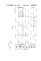
Images


Classifications
-
- G—PHYSICS
- G06—COMPUTING; CALCULATING OR COUNTING
- G06F—ELECTRIC DIGITAL DATA PROCESSING
- G06F9/00—Arrangements for program control, e.g. control units
- G06F9/06—Arrangements for program control, e.g. control units using stored programs, i.e. using an internal store of processing equipment to receive or retain programs
- G06F9/30—Arrangements for executing machine instructions, e.g. instruction decode
- G06F9/30003—Arrangements for executing specific machine instructions
- G06F9/30072—Arrangements for executing specific machine instructions to perform conditional operations, e.g. using predicates or guards
-
- G—PHYSICS
- G06—COMPUTING; CALCULATING OR COUNTING
- G06F—ELECTRIC DIGITAL DATA PROCESSING
- G06F9/00—Arrangements for program control, e.g. control units
- G06F9/06—Arrangements for program control, e.g. control units using stored programs, i.e. using an internal store of processing equipment to receive or retain programs
- G06F9/30—Arrangements for executing machine instructions, e.g. instruction decode
- G06F9/30145—Instruction analysis, e.g. decoding, instruction word fields
Definitions
- the invention relates to a pipelined digital processor which is described more particularly as a processor arranged for conditional operations.
- Stored program control digital computers typically include a memory, input-output circuitry, a controller and arithmetic section.
- the memory provides a source for a computer program and data to be operated on by the arithmetic section.
- the arithmetic section includes circuits which provide means for manipulating data in a predetermined manner.
- the controller provides control signals for regulating timing and transfers of data to be operated upon.
- the input-output circuitry provides means for transferring information between the computer and external devices.
- the arithmetic unit, or section includes a collection of specialized circuits capable of working simultaneously but altogether forming a general purpose organization. These specialized circuits operate independently, each performing a specific task in a general purpose procedure.
- the pipelined operation divides a process into several subprocesses which are executed by the individual specialized circuits. Successive ones of the subprocesses are carried out in an overlapped mode analogous to an industrial assembly line. New operands are applied at the input to the arithmetic section during each cycle. Different subsections of the arithmetic section perform their tasks in sequential order during subsequent cycles. A resultant is produced each cycle.
- Each specialized circuit performs its own task at the cyclic rate.
- Control of a pipelined computer, or processor presents particularly perplexing problems when operations are to be executed conditionally because instructions become stacked up in the pipeline during steady-state operation.
- a pipelined digital processor has been designed to transfer data words and instructions from memory to the arithmetic section and a control section in respective pipelined streams. These streams of data words and instruction words fill pipelines of circuits within the processor. As long as the processor operates normally, the pipelines of information are processed step by step through sections of the processor in a cyclical operation.
- the processor includes a source of instructions and data words.
- An arithmetic section processes one data word with another data word through selected processing subsections performing operations according to an expression, thereby producing a resultant data word.
- a destination receives the resultant data word from the arithmetic section.
- Control circuits decode a single conditional instruction word for controlling performance of a specific condition test during a first subsequent processor cycle.
- the control circuits further decoding another instruction word during the first subsequent processor cycle for controlling all processing sections operations during a second subsequent processor cycle.
- the specific condition test is performed by a circuit which compares conditions existing in the digital processor during the first subsequent processor cycle with information included in the conditional instruction for selectively disabling control of at least one section of the processor during the second subsequent processor cycle.
- FIGS. 1 and 2 when positioned as shown in FIG. 3 form a block diagram of a pipelined digital signal processor
- FIG. 4 is a timing diagram
- FIG. 8 is a processor function chart for a conditional operation
- FIG. 9 is a logic diagram of some control circuits.
- FIG. 10 is a logic diagram of other control circuits.
- FIGS. 1 and 2 there is shown the overall architecture of a pipelined digital signal processor.
- a read only memory 100 stores instructions and fixed data words. Instructions are transferred from the read only memory by way of a common data and control bus 101 to instruction registers IR-C, IR-L,M,N, and IR-S,T. Parts of instructions are distributed to the instruction registers. Fixed data words, or coefficient words, are transferred from the read only memory by way of the common data and control bus 101 to a coefficient register 102.
- the register 102 is labelled REG X because the coefficients are identified hereinafter by the symbol x.
- a random access memory 105 stores variable data words which may be stored therein either from an external source or from the output of the arithmetic section of this processor.
- the variable data words are transferred from the random access memory by way of the common data and control bus 101 to a variable data register 106.
- the register 106 is labelled REG Y because variable data words are identified hereinafter by the symbol y.
- the random access memory may store coefficients used in place of fixed data words as well as the variable data words.
- Registers 102 and 106 respectively, store a sequential stream of coefficient words and variable data words which are operands applied as inputs to an arithmetic section 110. These sequences of operands are processed in a pipeline fashion through a multiplier subsection 112, an accumulator subsection 115 and a rounding and overflow circuit subsection 116. A rounded output word is produced in a register 118 that is labelled REG W because rounded output words are identified by the symbol w hereinafter.
- An output selector circuit 120 is included within the arithmetic section for choosing as an output word from the arithmetic section to the data bus 101 either the variable data word y stored in register 106 or the rounded output word w stored in register 118.
- the rounded output word w is a resultant of some process performed by the arithmetic section.
- the chosen output word can be transferred from either the register 106 or the register 118 by way of the common data and control bus 101 to a writeable destination, such as in the random access memory 105.
- instructions for the digital signal processor are stored in read only memory 100.
- a single instruction automatically is read out of read only memory from a location having an address produced by an address arithmetic unit, or section, 124.
- the address from a program counter register PC in the address arithmetic section is applied by way of an address bus latch 145 and an address bus 128 to the address circuitry of the read only memory.
- Read only memory responds during each processor cycle by sending the single instruction thus fetched by way of the common data and control bus to the various control field, or instruction, registers IR-C, IR-L,M,N and IR-S,T associated with different sections of the processor. Registers IR-C and IR-L,M,N receive the same information concurrently.
- Each instruction, or opcode, used in the digital signal processor includes a plurality of control fields, or control messages, each of which is given a designation such as l, m, n, s and t to be used hereinafter.
- the control field register IR-L,M,N associated with arithmetic section 110 receives some of the fields, such as instruction fields l, m and n, respectively associated with control of multiplying, accumulating and rounding operations.
- the control field register IR-S,T associated with the address arithmetic section 124, receives instruction fields s and t which relate to control of address register modification for controlling the fetching of operands x and y and the storing of the output word chosen by the selector circuit 120.
- the address arithmetic section 124 includes two sets of registers 141 and 142, the address bus latch 145, an adder 147 and an adder latch 150 interconnected by some busses.
- One set of registers 141 is arranged to store memory addresses.
- An address stored in register RX can be used for accessing a coefficient word stored in a location in either random access memory or read only memory.
- An address stored in register RY can be used only for accessing a variable data word stored in a location in random access memory.
- An address stored in the register RD can be used for writing a resultant data word into a destination, such as a location in a random access memory.
- An address stored in the program counter register PC is used for accessing the next instruction or fixed data word from the read only memory.
- the second set of registers 142 is arranged to store variable increment values to be used for incrementing automatically addresses stored in registers RX, RY and RD. Alternatively, the stored addresses may be incremented by one of a set of fixed value increments.
- auxiliary instructions Operations of the digital signal processor are controlled by two types of instructions. Normal instructions are used most of the time. They control the performance of arithmetic operations during signal processing. Another type of instruction, used occasionally, is called an auxiliary instruction. One specific auxiliary instruction controls the loading of an address register or an address increment register in the address arithmetic section.
- the processor can run a valid program for processing digital signals.
- Most of the instructions used for processing signals are normal arithmetic instructions.
- Information in each of the registers RX, RY, RD, PC, RI, RJ and RK can be set to any specific value by an auxiliary instruction.
- a first instruction to load address register RY specifies that some processor register is to be loaded or set.
- a control field c contains the required information. This control field c is stored in an instruction register IR-C during the instruction fetch cycle.
- the control field and value field are transferred from memory by way of the common data and control bus 101 to the control field register XSR and the value field register XSL.
- the control field in the register XSR is decoded in a decoder 157 to select the proper address register. From register XSL the value to be loaded into the address register RY is applied to the registers 141 and 142 through a selector circuit 158 and a bus 160 in the execution cycle of the first instruction.
- a second instruction to load increment register RI specifies that a processor register is to be loaded or set.
- a fixed data word similarly associated with the second instruction provides a control field to identify the register to be set and a value field to establish the value to be loaded.
- the fields of the fixed data word are applied from the register XSR through the decoder 157 and the bus 137 to determine the increment register selected in the set of registers 142 and from the register XSL through selector 158 and bus 160 to establish the value to be loaded in the selected increment register during the execution cycle of the second instruction.
- control fields s and t from the instructions are stored in the instruction register IR-S, T when that instruction is fetched. These fields to be processed are decoded in a decoder 152 during the next processor cycle with the decoded information being latched in an AAU control circuit 154. This decoded information is applied over a bus 135 to the sets of registers 141 and 142 during the instruction execute cycle, or second processor cycle, after the fetch. Both an address register and an increment register or a fixed increment are selected by the information on bus 135. The address is applied to the address bus latch 145 and to the input of an adder 147.
- the increment value simultaneously is applied to the other input of the adder 147, which increments the address and stores it for one machine state in an adder latch 150.
- the incremented address is applied by way of a bus 136 to the set of address registers 141.
- part of the information in the fields s and t is applied through a single machine state delay in a delay circuit 155.
- This delayed information provides selection information for determining which of the address registers 141 is to be written after the just described addressing operation.
- the delayed information is decoded in a decoder 157 and applied over a bus 137 to the address registers 141.
- the incremented address stored in the adder latch 150 is written into the selected address register thus post modifying the address.
- the above described operation for writing a post modified address back into an address register may be preempted by the register set operation. Preempting is accomplished by the decoder 157 in response to information applied from logic circuit 122 by way of a path 138, AAU control circuit 154 and delay circuit 155.
- the information for selecting the address register is applied from register XSR through the decoder 157 and bus 137 to the address register set 141. Simultaneously from the register XSR, information is applied through decoder 157 and bus 137 for selecting information on bus 160 in lieu of information on bus 137.
- the address arithmetic section 124 transmits addresses by way of the address bus latch 145 for accessing locations in memories 100 and 105, generates new addresses in the adder 147 and sets the address registers RX, RY, RD and PC.
- FIG. 4 the diagram shows that addresses are transmitted to memory as a series of four addresses being transmitted during each processor cycle.
- One of the addresses is transmitted during each of four machine states during each processor cycle.
- the first address transmitted during the first machine state is the address stored in the program counter register PC. As indicated in FIG. 4, this address is transmitted automatically during the first machine state of each processor cycle.
- the second address transmitted during the second machine state is the address stored in register RD or in register RX.
- the third address transmitted during the third machine state is the address stored in register RX or in the program counter register PC.
- the fourth address transmitted during the fourth machine state is the address stored in register RY.
- Each address transmitted by the address arithmetic section is latched in the address bus latch 145 during one of the mentioned machine states of the processor cycle. Also during those machine states, the addresses are incremented in the address arithmetic unit adder 147 by an increment value that is read out of one of the increment registers RI, RJ and RK or in the case of the address from register PC, the address is incremented by +1. These incrementing operations are accomplished during the same machine state that the address is latched.
- Identification of the selected address and increment registers is accomplished by applying the appropriate control fields to the instruction register IR-S,T prior to the addressing operation so that the appropriate coding is applied to access circuitry for both the address and the increment registers during the machine state that the address is to be transmitted. Both the address and the value of the increment are read out and are summed by the adder 147. The resulting incremented address is stored in the adder latch 150 while the address is being transmitted from the address bus latch 145.
- Coding for identifying whichever address register was selected is transferred through the delay circuit 155 to the decode register circuit 157.
- Delay and decoding are designed so that the incremented address stored in the adder latch 150 can be written into the address register from which the transmitted address was fetched.
- the transmitted address is post-modified or post-incremented during the processor cycle when it is transmitted to the memories 100 and 105.
- Coefficient words x and variable data words y are operands received from the memories by way of the common data and control bus 101 into coefficient word register 102 and the variable data word register 106.
- coefficient word x is fetched over the common data and control bus 101 into the coefficient word register 102, as shown in FIG. 4.
- variable data word y is fetched over the common data and control bus 101 into the variable data word register 106, as shown in FIG. 4.
- the rounded output words w also are operands for some operations and are stored in the register 118. A new operand is received into each of those registers during every processor cycle of a normal instruction.
- the arithmetic section 110 includes three subsections which are independently controllable in response to different control fields l, m and n.
- the fields l, m and n are stored in an instruction register IR-L,M,N.
- those fields are decoded in a decoder circuit 113 and the result stored in register REG F.
- this information is transferred to an AU control circuit 114 for supplying control signals to various subsections of the arithmetic section. This latter processor cycle is the execution cycle of the instruction.
- Decoder circuit 113 is a gated decoding circuit producing three separate outputs. Each of those outputs originates from a decoding logic circuit and can be either a "1" or a "0". Each of those three outputs is applied as an input to a separate AND gate. The other input to each AND gate is a gating signal from the logic circuit 122. This gating signal from circuit 122 is either a "0" for enabling all three AND gates or a "1" for disabling all three AND gates.
- the AND gates When the AND gates are enabled as a result of a condition being met during execution of a conditional instruction, the output signals from the decoding logic circuit are gated through the AND gates and are applied to respective memory cells in the register REG F.
- the AND gates When the AND gates are disabled as a result of a condition not being met during execution of a conditional instruction or because an unconditional instruction is being executed, the three outputs from the decoding logic circuit are blocked and therefore are not applied to the cells of the register REG F.
- the AND gates of the decoder circuit 113 are enabled or not depending upon whether a condition, specified by the conditional instruction being executed, is met or not as described subsequently.
- Information stored in the three cells of the register REG F is applied to three inputs of the arithmetic control circuit 114.
- those three inputs are gated by three AND gates which are enabled once during each processor cycle by a processor clock signal which is applied by way of a lead 228.
- Outputs of the AND gates are applied respectively to the circuits of the multiplier section 112, to the circuits of the accumulator section 115, and to the circuits of the rounding and overflow section 116.
- the signals "1" enable the circuits of the sections to which they are applied.
- the signal "0" disables the circuits of the section to which it is applied.
- the circuits of one section may be disabled at a time when a specified condition is met during execution of the conditional instruction.
- the control signals provide information relating to which choices are to be made from processing options available in each of the subsections.
- the multiplier subsection 112 typically generates a product of two operands during each processor cycle. In a typical multiplication, one operand is the coefficient word x and the second operand is either the variable data word y or the rounded output word w.
- All of the outputs from the register REG A of the accumulator section 115 in FIG. 1 are applied through the path 225 to the arithmetic unit control circuit 114, as shown in FIG. 9.
- the path 225 is shown to include forty leads.
- flags, or status signals are generated by a flag circuit 230 which includes NOR gates 232 and 234.
- the NOR gate 232 has a separate input for each of the 40 outputs of the register REG A in the accumulator section 115. When the register REG A stores all zeros, the output of the NOR gate 232 is a "1" because of its output inversion.
- a single lead designated MSB is a "1" indicating that the condition of the accumulator is the contents a are less than zero, i.e., a ⁇ 0.
- the output of the NOR gate 232 is a "0" and the most significant bit MSB is "0”
- the output of the NOR gate 234 is a "1" indicating that the condition of the accumulator is the contents a are greater than zero, i.e., a>0.
- Coefficient word x is a 16-bit word. These sixteen bits are taken into the register 102 from the most significant bit lines of the common data and control bus.
- a selection circuit 162 scans the sixteen bits of the coefficient word, from the least significant bit to the most significant bit, four bits at a time during each of the four machine states in every processor cycle.
- Another selection circuit 163 concurrently selects either a 20-bit variable data word y or a 20-bit rounded output word w.
- Booth logic circuit 165 responds to the successive 4-bit nibbles to produce control signals for the generation of partial products.
- the output from the Booth logic circuit 165 during every machine state is latched into a register 166. This output is applied to a circuit 168 which produces the the partial products by data selection.
- An adder 170 sums the partial products with the prior sum and carry information storing a resulting 36-bit intermediate operand, or product word p, in a product register P.
- Associated registers S and C respectively store the sum and carry information produced during each processor cycle.
- the product register P receives a new intermediate operand, or product word, p during every processor cycle of normal instructions. This product word p is applied by way of a bus 172 as an intermediate operand to the input of the accumulator subsection 115.
- the product word p is added with a 40-bit resultant output word a that may be shifted by a circuit 174 prior to application as an input to an adder circuit 175.
- the adder circuit 175 produces sum and carry information which is stored in register 177.
- the sum and carry information is stored in register 177 during every processor cycle. Carries are resolved by carry-look-ahead logic in adder 178.
- Output from adder 178 is applied to an input of a logic circuit 180 together with the resultant output word a to generate the next subsequent value of the 40-bit resultant output word a to be stored in register A.
- Such a resultant output word is produced and stored in register A during each processor cycle of a normal instruction.
- a portion of the resultant output word a is applied as an input to the rounding and overflow circuit subsection 116 in 10-bit slices. These slices are clocked through rounding circuit 182 and an overflow logic circuit 184 to the 20-bit rounded output register W in three consecutive machine states of each processor cycle.
- state 3 shown under processor cycles i+1 and i+2 in FIG. 4, the value in the register W may be corrected for overflow if the value in the register A is too large to be represented in the 20-bit register W.
- state 0 of the next processor cycle shown in FIG. 4, the rounded output word can be transferred through the common data and control bus 101 to a destination, such as a location in the random access memory 105 where it is stored.
- the three subsections (multiplier, accumulator and rounding) of the arithmetic section accomplish their basic operations in one processor cycle each. Outputs of the subsections are stored in registers every processor cycle so that the next subsection in line has a stable input to commence the next subsequent processor cycle.
- Control of the arithmetic section 110 and of the address arithmetic section 124 is accomplished by a pipelined stream of instructions applied from the memory 100 through the common data and control bus 101.
- a single instruction is read out of memory during state 3 of each processor cycle of operation.
- Such an instruction includes several instruction fields, or control messages, l, m, n, s and t.
- Fields l, m and n are transferred through the common bus 101 to the register IR-L, M, N for controlling the subsections of the arithmetic section 110.
- Fields s and t are transferred through the common bus 101 to the register IR-S,T for controlling selection and incrementation of addresses stored in the registers RX, RY, RD and PC.
- a complete normal assembly language instruction includes all of the information required to perform a desired arithmetic operation.
- Assembly language instructions for the digital signal processor are designed to represent the control for access to the memory and the control for operation of the arithmetic subsection and of the address arithmetic subsection.
- the arithmetic subsection continuously performs multiplication and addition operations.
- the normal arithmetic section operations are characterized by the following general expressions:
- x is a 16-bit wide coefficient word usually fetched from read only memory.
- the coefficient word x also could be fetched from random access memory or from an input/output circuit 200 and ordinarily has a value for all arithmetic operations.
- y is a 20-bit wide data word normally fetched from random access memory. Such a data word also could be fetched from the input/output circuit 200.
- a represents the 40-bit wide contents of an accumulator register A.
- the least significant thirty-six bits are used to accumulate the product of a 16-bit by 20-bit multiplication.
- the four most significant bits provide overflow protection for the accumulation operation.
- w is a 20-bit wide rounded or truncated output of the accumulator.
- the least significant bit of the rounded output w corresponds with the bit that is fourteenth from the least significant bit of the contents a of the accumulator. This correspondence of bits is consistent with an assumption that the data word y and the rounded output w are integers and that the coefficient word x usually is restricted within the bounds -2 ⁇ x ⁇ 2.
- f describes a function of either the data word y or the rounded output w.
- Such function can be the actual value, the sign, or the absolute value of either one of the variables y or w.
- f a generally describes a function of the contents a of the accumulator, such as a, -a, 0, 2a, etc.
- the variables x, y, w and p are contained in arithmetic section registers X, Y, W and P, respectively.
- Each of these three operations is completed during one processor cycle of the digital signal processor.
- the coefficient word x has a value and a multiplication forms the product p.
- all three types of operations are performed concurrently by different subsections of the arithmetic section. For some instructions one or more of the three operations may not occur.
- the operation performed by one subsection during one processor cycle is a partial evaluation of a different general expression than the expressions concurrently being evaluated in the other subsections.
- Assembly language instructions are converted to machine language instructions which are stored in the memory for actually controlling the digital signal processor. Because the operations are dependent upon one another and because all of the operations occur concurrently within the processor, it is important to know at all times what is stored in various registers and what operation is to be performed thereupon.
- a choice of destination is made.
- the word to be written to the destination is chosen from either the rounded output word w or the data word y.
- the chosen word can be written into the random access memory or into the input/output circuit.
- the specific destination of the selected word is given.
- the value of the rounded output w is the value determined by the last rounding of the resultant word a as performed in a preceding instruction. If data word y is to be written and a source for data word y is specified, the first step in execution of the instruction moves the data from the specified source into the data register Y. Thereafter any writing of this new value for data word y can occur.
- Table I summarizes the normal assembly language instructions that a programmer would use for preparing an assembly language program.
- the syntax of a language called C is used as the assembly language which is described in a text entitled, The C Programming Language by B. W. Kernighan et al, Prentice-Hall, Inc., 1978.
- Each complete instruction is formed by choosing four statements, one statement from each column of Table I starting with the lefthand column and working toward the right. In the two leftmost columns, the word NOTHING is listed as a valid choice. When the word NOTHING is selected as a part of a complete instruction, the corresponding space in the instruction is left blank. Every complete assembly language instruction is terminated by a semicolon.
- *rd++i means that rd, which is the address of the location in random access memory pointed to by the contents of register RD, is post incremented by the contents i of the register RI.
- the symbol VALUE represents a number that appears as an argument of an instruction, i.e., the 16-bit word immediately following the opcode in the read only memory. Such argument is addressed by the address stored in the program counter register PC.
- the coefficient word x is addressed by the contents rx of the register RX.
- the notation *(rom+rx . . . ) is used to indicate that the contents rx of the register RX point to read only memory rather than the random access memory.
- the symbol &LABEL represents that the value read from memory source x is an address associated with a label in the program.
- l means an instruction field for controlling the formation of a product.
- m means the instruction field for performing an accumulation.
- n means an instruction field for controlling a transfer operation from register A to register W with the required rounding.
- s represents an instruction field identifying a write destination.
- the destination is a memory location specified by the address stored in register RD. That address is post-incremented and the result stored in the register RD.
- t means an instruction field to fetch information from an address stored in an address arithmetic unit register, post-increment that address and store it back into that same register.
- the resulting skewed assembly language statement which appears diagonally on the time line of the leftmost column, is stated together with skewed assembly language statements representing other general mathematical operations.
- the resulting pieces of different statements which appear in the same row, or during the same interval such as interval i, form an assembly language instruction.
- the assembly language instruction the different pieces of information in the same interval are separate fields of that assembly language instruction. Each of these fields controls a separate subsection of the processor for performing a step in the process of evaluation, as described by a portion of one of the general mathematical expressions.
- An assembler program which runs on a general purpose computer, operates on each assembly language instruction by moving the source fields two processor cycles earlier in the program than the rest of the fields in that same assembly language instruction. This moving of the source fields is done to every assembly language instruction in the program.
- the resulting time line for the foregoing assembler statement, as skewed by the programmer and the assembler, will appear as follows:
- FIGS. 5 and 6 there is shown a time line diagram indicating how data is processed in the digital signal processor.
- the diagram presents the flow of data through various subsections of the processor during the evaluation of one general mathematical expression together with parts of other mathematical expressions.
- I i is a machine language instruction fetched from read only memory during a processor cycle, or interval, i and decoded within the processor during a processor cycle, or interval, i+1.
- the instruction I i affects operation of sections of the processor during a processor cycle, or interval, i+2.
- each instruction contains the fields, or control messages, l, m, n, s and t.
- I i (t) represents the field t in the machine language instruction I i for controlling the fetching of operands x i+3 and y i+3 . These fetches take place during the interval i+3.
- I i (l) represents the field l in the machine language instruction I i for controlling the computation of a product, or intermediate operand, p i+2 during the interval i+2.
- the product p i+2 is a function of the operands x i+1 and y i+1 .
- I i (m) represents the field m in the machine language instruction I i for controlling the accumulation of output from, or desired resultant word, a i+2 during the interval i+2.
- the resultant word a i+2 is a function of the last prior resultant word a i+1 and a product p i+1 previously computed.
- I i (n) is a field n in the machine language instruction for controlling the transfer of a rounded output word w i+2 during interval i+2.
- Rounded output w i+2 is a function of the last prior rounded output w i+1 and the resultant word a i+1 of the accumulator.
- I i (s) is a field in the machine language instruction for controlling the storing of the rounded output word w i+1 and the modification of register stored addresses u i+2 during the interval i+2.
- the modified addresses are a function of the prior address u i+1 and field I i (s).
- the updated memory state M i+2 is a function of the field I i (s), the prior memory state M i+1 , register stored addresses u i+1 and the rounded output word w i+1 .
- I i (s,t) is a combination of fields s and t within the machine language instruction.
- the fields control the modification of register stored addresses u i+2 during the interval i+2.
- the modified addresses u i+2 are also a function of the address u i+1 .
- x i and y i are operands fetched from memory during the interval i, under control of the field t of the instruction I i-3 fetched from memory during the interval i-3.
- Instruction I i-3 is decoded during interval i-2 and controls processing during interval i-1 wherein the addresses for operands x i y i are produced.
- these operands are accessed from memory during interval i. They are processed through the multiplier during the interval i+1 under control of the field l of the instruction I i-1 , which is fetched during the interval i-1. This produces the intermediate operand or product p i+1 .
- p i+1 represents the product formed by the multiplier during the interval i+1. This product is an intermediate operand which is used as an input to the accumulator for its operation during the interval i+2.
- Product p i+1 is formed in register P under control of the field I i-1 (l).
- the multiplier and multiplicand are the operands x i and y i .
- a i+2 represents the contents of the accumulator during the interval i+2. This is the desired resultant word a i+2 for the expression being evaluated.
- the word a i+2 is an input for the rounding and output circuit subsection for the interval i+3. The rounding operation occurs under the control of the field I i+1 (n).
- w i+3 represents rounded output word w which is available in the register W and which can be stored into writeable memory during the interval i+4 under the control of the field I i+2 (s).
- each column in the chart represents a different processor cycle, or time interval, of the processor.
- Information in each column is closely related to some machine language instruction.
- Each row represents activities of a different processor subsection performing its assigned functions during operation of the digital signal processor.
- each row of the chart represents a different activity, we shall define those activities.
- the first row below the processor cycle headings indicates storage activities, i.e., memory fetches and stores.
- the second row presents the time at which instructions are decoded within the digital signal processor.
- the third row shows the computing of the product p by the multiplier subsection of the processor.
- the fourth row presents the accumulating of the resultant word a by the accumulator subsection of the processor.
- Row five presents activities of the rounding and overflow subsection of the processor, which produces the rounded output word w.
- the sixth row discloses activities associated with modifying addresses used for fetching data for the arithmetic processes.
- a first step in the processing of a general arithmetic expression is the fetching of operands for a multiplication.
- information relating to this fetch operation is placed by the assembler program into an interval earlier than the information associated with control of the multiplication operation.
- every machine language instruction includes a control field for a fetch operation that fetches information from memory for processing to be controlled by a subsequent machine language instruction.
- each instruction shown in the processor function chart is similarly designated in accordance with the interval during which the instruction is fetched from memory.
- each instruction, shown in FIGS. 5 and 6 includes several fields of control information. Those fields l, m, n, s and t are shown in parentheses associated with the instruction in the first row representing the fetching and storing operations. A separate field or separate fields of an instruction are shown in other rows of the chart, e.g., I i (l) in the row for computing products and I i (s,t) in the row for modifying addresses.
- the just fetched instruction I i-3 is decoded by the processor, as shown in the emphasized box in the second row representing the decoding of instructions.
- a fetch operation for the operands x and y, identified by the instruction I i-3 begins during the interval i-1.
- the fetch operation begins using an address specified in the instruction field I i-3 (t). When that address is used, it is modified and stored back in the address arithmetic section as a function of the instruction field I i-3 (s,t) and the prior state u i-2 of the registers in the address arithmetic section. This modification of addresses is shown in the emphasized box under the interval i-1.
- Fetch of those operands x and y is concluded during interval i when the specific operands x i and y i , identified by the instruction I i-3 , are read out of memory and are transferred by way of the common data and control bus respectively to registers REG X and REG Y. These fetch operations are shown in the emphasized box under the interval i.
- the operand x i typically is read out of read only memory, and operand y i typically is read out of random access memory.
- the address pointers, or the addresses stored in registers RX and RY, which were updated in the prior interval i-1 are used for accessing the operands from memory during the interval i.
- the first arithmetic operation to be performed on the operands x i and y i occurs during interval i+1.
- the multiplier subsection responds to the instruction field I i-1 (l) for computing an intermediate operand, or product, p i+1 , as shown in the emphasized box under interval i+1.
- Such product p i+1 is shown as a function of the operands x i and y i and of the instruction field I i-1 (l).
- Instruction I i-1 which includes the field I i-1 (l), is fetched from memory during the interval i-1, is decoded during interval i and controls sections of the processor during interval i+1.
- the next step in evaluating the general expression is processed in the accumulator during interval i+2. This is shown in FIG. 6 in the fourth row representing the accumulation of the resultant word a in an emphasized box under the column designated interval i+2.
- a resultant word a i+2 is shown to be a function of the prior resultant word a i+1 stored in the accumulator, of the just described intermediate operand, or product, P i+1 and of the instruction field I i (m).
- a final step in processing the general expression is a writing of the rounded output w i+3 into memory during interval i+4. This is shown in the emphasized box in the first row of the chart under the interval i+4.
- Writing a new memory state M i+4 is a function of the memory state M i+3 for interval i+3 of the last prior address register state u i+3 , of the last rounded output w i+3 just described, and of the instruction field I i+2 (s) which was fetched during interval i+2 and decoded during interval i+3.
- Rounded output w i+3 contained in the rounded output register at the end of interval i+3 is transferred by way of the common data and control bus either to the random access memory or to a buffer in the input/output circuitry during interval i+4.
- the address arithmetic section registers are updated based on information in the instruction fetched during interval i+2.
- the information used is included in the fields I i+2 (s,t) of the instruction I i+2 that is fetched during interval i+2 and is decoded during interval i+3.
- interval i+2 it is noted that the instruction I i which was fetched during interval i controls the multiplier subsection, the accumulator subsection and the rounding overflow subsection of the arithmetic section. This results from the instruction I i being fetched in interval i, decoded in interval i+1 and used for control during interval i+2. No parts of the instruction I i remain for controlling subsections of the arithmetic section during subsequent intervals, as in prior pipelined control arrangements. Most of the column representing interval i+2 is emphasized with heavy lines so that the reader readily can find several fields of the instruction I i for controlling subsections of the arithmetic section during interval i+2.
- a resultant word a i+2 which is formed during that same interval i+2 is a function of an earlier resultant word a i+1 and an earlier product p i+1 .
- This resultant word a i+2 is a resultant word evaluated for a different general expression than the general expression being evaluated by forming the product p i+2 .
- This concept can perhaps be better understood by the realization that the emphasized boxes forming a diagonal from the top of the column designated processor cycle i down to the fifth row in the column designated processor cycle i+3 relate to the evaluation of one general expression. A similar diagonal, shifted one interval to the right in each column, relates to the evaluation of another different general expression.
- program counter is incremented by the fixed increment +1 and is used to address the next fixed data word during state 2 of processor cycle i+2.
- program counter is incremented by +1 and is used to address instruction I i+3 in state 0 of the processor cycle i+3 and so on until the end of the instruction sequence.
- program counter is set, by an auxiliary register set instruction, to the address of the first instruction in the sequence.
- the algorithm realized by the condition test and execution of alternative operations that are dependent upon the outcome of the test, may be realized as well by a sequence of one or more instructions that either is executed or is not executed. If this sequence is short, the overall savings in processing time may be large when compared with using the conditional program transfer technique of the prior art for achieving the same result.
- conditional operations occurring in digital signal processing frequently can be realized with the use of a sequence of one or more instructions that either is executed or not. Therefore the digital signal processor has been designed to process efficiently conditional operations in this manner. The concept used, however, has wider applicability to digital processors generally.
- a conditional instruction causes the processor to perform a condition test operation which is a non-arithmetic auxiliary operation.
- a condition test operation which is a non-arithmetic auxiliary operation.
- a choice of destination is made.
- the word to be written to the destination is chosen from either the rounded output word w or the data word y.
- the chosen word can be written into the random access memory or into the input/output circuit.
- the specific destination of the selected word is given.
- Each conditional instruction is assembled as a 16-bit opcode word followed by a 16-bit argument.
- the format for a conditional instruction is ##STR3## where c, s and t are control fields, as in the normal arithmetic instructions. Fields s and t have the same meaning.
- Control field c provides control information for the conditional operation. That information includes what operation is to be performed together with the condition to be tested.
- a processor address or increment register is set if the specified condition is true.
- the next arithmetic section operation is performed if the condition is true.
- the third choice is that the next write operation is performed if the condition is true. For every conditional instruction, the mentioned operations do not occur if the condition is false. Other operations of each conditional instruction occur whether or not the condition is false.
- Operations which are subject to the condition test are the operations specified in the instruction next following the conditional instruction in the pipeline.
- Each conditional instruction processed by the digital signal processor is fetched from the read only memory 100 and is transferred over the data bus to the instruction registers.
- the control fields s and t are stored in the instruction register IR-S,T as previously described.
- Control field c is stored in instruction register IR-C and in instruction register IR-L,M,N.
- FIG. 8 the operation of the arrangement of FIGS. 1 and 2 will be described performing a conditional operation. Most of the conditional operation occurs much like a routine normal operation. Therefore emphasis will be placed upon those portions of the operation which differ from a routine normal operation. The reader is referred back to the preceding descriptive material for completeness.
- conditional instruction I i (c,s,t) that is fetched during processor cycle i and is decoded in processor cycle i+1.
- the conditional instruction I i (c,s,t) is positioned in the pipeline to affect a normal arithmetic instruction i i+1 (l,m,n,s,t) which is fetched during processor cycle i+1, decoded during processor cycle i+2 and is conditionally executed during processor cycle i+3.
- Fields s and t of instruction I i (c,s,t) control data fetches and a write operation during the interval i+2.
- the state u i+2 of the registers in the address arithmetic section is updated during interval i+2 as a function of the control fields I i (s,t) and of the prior state u i+1 of those registers.
- a write memory operation M i+2 that occurs durin cycle i+2 is similar to the operation previously described with respect to the normal arithmetic instruction. Because the conditional instruction is an auxiliary instruction, the arithmetic section 110 is idled during interval i+2 which is the usual execution cycle for this instruction.
- multiplier register P accumulator register A and rounded output register W retain their respective data from the last prior cycle.
- Intermediate operand p i+2 equals p i+1
- resultant a i+2 equals a i+1
- the rounded output word w i+2 equals w i+1 .
- Control field I i (c) which is stored in the instruction register IR-C during interval i includes one part identifying what condition is to be tested and a second part identifying what operation is to be controlled in dependence upon the test outcome of the condition.
- the two parts of the control field I i (c) are decoded in circuits 211 and 212 and are stored in registers 213 and 214, respectively.
- the first decoded part of control field I i (c) that is stored in registers 213 is applied to a comparator 215 establishing what condition is being tested. Simultaneously, the status of conditions, or flags, V i+2 from the arithmetic section control 114 are applied by way of lead 103 to the comparator 215. Thus the status of the conditions of the arithmetic section are tested. Comparator 215 produces a condition true or a condition false signal on lead 221 through which the resulting signal is applied as a conditional control on logic circuit 122.
- the second part of control field I i (c) that is stored in register 214 is applied to the logic circuit 122 for generating further control signals.
- the logic circuit 122 which is enabled or disabled under the control of the conditional signal on lead 221 produces the further control signals that are dispersed to the circuit DECODE F, the address arithmetic section control 154, the random access memory 105 and the input/output circuit 200.
- the latch circuit 214 includes three cells, or stages, for storing three bits of information from the decoding circuit 212.
- the bits determine, respectively, whether a conditional arithmetic unit operation, a conditional write operation or a conditional set an address register operation is to be accomplished by a conditional instruction. Only one of these three bits is a "1" for any conditional instruction.
- Logic circuit 122 includes three AND gates for gating outputs from the latch circuit 214 to the various other circuits in FIGS. 1 and 2 as indicated. A gating signal for the three AND gates is applied from the comparator circuit 215 of FIG. 2 by way of lead 221. The result of the conditional operation is held at the output of the logic circuit 122 for enabling or disabling the various sections of the processor during interval i+3.
- Normal arithmetic instruction I i+1 (l,m,n,s,t), which is to be affected by the conditional instruction I i (c,s,t), is fetched during interval i+1 and is decoded during the cycle i+2. Without the preceding conditional instruction this instruction would control the processor during interval i+3. Data fetches for interval i+3 occur as usual.
- conditional instruction I i (c,s,t) is a conditional arithmetic section execute
- only arithmetic unit operations are conditionally executed during the interval i+3. Writing memory is not inhibited at this time. If the condition is true for the conditional arithmetic section execute instruction, a new product p i+3 , resultant word a i+3 and rounded output word w i+3 are produced. If the condition is false, control of the arithmetic section is disabled and no new product, resultant word or rounded output word is formed.
- the registers P, A and W retain values from the last prior interval. All other normal processor operations occur during interval i+3.
- conditional instruction I i (c,s,t) is a conditional write instruction
- only the memory write and output write operations are affected during interval i+3. Operations of the arithmetic section are not inhibited.
- the condition is true for the conditional write instruction, the memory write operation M i+3 or output write operation occurs. If the condition is false, control of the write operation is disabled and the memory retains its state M i+2 from the prior interval. Writing to memory or output is controlled by control field I i , as discussed previously for normal instructions. Whether the condition is true or false, all other processor operations occur normally during interval i+3.
- conditional instruction I i (c,s,t) is a conditional register set instruction
- the register set instruction is an auxiliary instruction, there will be no activity in the arithmetic section. Memory or output write may proceed without interference as specified by control field I i (s). If the condition is true, the register designated by the register select field of the fixed data word, associated with the register set instruction, is loaded with the value in the value field of that data word, as explained previously. If the condition is false, control of the register set operation is disabled and the register contents are not changed by the register set instruction.
Abstract
Description
x·f(y)+f.sub.a (a)→a{→w}
x·f(w)+f.sub.a (a)→a{→w},
              TABLE I
______________________________________
NORMAL ASSEMBLY LANGUAGE INSTRUCTIONS
______________________________________
NOTHING   NO-      a=p        p= XSRC*YSRC
DEST=y    THING    a=p+a     p=XSRC*w
DEST=YSRC w=a      a=p-a     p=XSRC*c
DEST=w             a=p+2*a   p=XSRC*abs(YSRC)
                   a=p+8*a   p=XSRC*abs(w)
                   a=p+a/2   p=XSRC*c*sgn(YSRC)
                   a=p+a/8   p=XSRC*c*sgn(w)
                   a=p&a
______________________________________
______________________________________
XSRC               YSRC
______________________________________
x(old x)           *ry++i
VALUE (immediate x)
                   *ry++j
*rx++i             *ry++k
*rx++j             ibufy
*rx++k
*rx
*rx--
ibufx
*(rom+rx++i)
*(rom+rx++j)
*(rom+rx++k)
&LABEL
______________________________________
x·f(w)+f.sub.a (a)→a{→w}
______________________________________
s          n      m          l,t
______________________________________
*rd++j=w   w=a    a=p+a      p=*rx++i* *ry++k;
______________________________________
______________________________________
Time s          n      m      l,t
______________________________________
i                             p=*rx++i* *ry++k;
i+1                    a=p+a
i+2             w=a
i+3  *rd++j=w
______________________________________
______________________________________
Time s          t             n    m      l
______________________________________
i-2             x=       y=
                *rx++1   *ry++k
i-1
i                                           p=
                                            x*y
i+1                                  a=p+a
i+2                             w=a
i+3  *rd++j=w
______________________________________
              TABLE II
______________________________________
CONDITIONAL INSTRUCTIONS
______________________________________
NOTHING          if (CONDITION) doset ( )
DEST = YSRC      if (CONDITION) doau ( )
DEST = w         if (CONDITION) dowt ( )
______________________________________
______________________________________
CONDITION   Description
______________________________________
a==0        Accumulator contents a equals zero.
a > 0       Accumulator contents a is greater than zero.
a < 0       Accumulator contents a is less than zero.
______________________________________
Claims (3)
Priority Applications (1)
| Application Number | Priority Date | Filing Date | Title |
|---|---|---|---|
| US06/401,350 US4539635A (en) | 1980-02-11 | 1982-07-23 | Pipelined digital processor arranged for conditional operation |
Applications Claiming Priority (2)
| Application Number | Priority Date | Filing Date | Title |
|---|---|---|---|
| US12005980A | 1980-02-11 | 1980-02-11 | |
| US06/401,350 US4539635A (en) | 1980-02-11 | 1982-07-23 | Pipelined digital processor arranged for conditional operation |
Related Parent Applications (1)
| Application Number | Title | Priority Date | Filing Date |
|---|---|---|---|
| US12005980A Continuation-In-Part | 1980-02-11 | 1980-02-11 |
Publications (1)
| Publication Number | Publication Date |
|---|---|
| US4539635A true US4539635A (en) | 1985-09-03 |
Family
ID=26818020
Family Applications (1)
| Application Number | Title | Priority Date | Filing Date |
|---|---|---|---|
| US06/401,350 Expired - Lifetime US4539635A (en) | 1980-02-11 | 1982-07-23 | Pipelined digital processor arranged for conditional operation |
Country Status (1)
| Country | Link |
|---|---|
| US (1) | US4539635A (en) |
Cited By (23)
| Publication number | Priority date | Publication date | Assignee | Title |
|---|---|---|---|---|
| US4656578A (en) * | 1983-09-16 | 1987-04-07 | International Business Machines Corporation | Device in the instruction unit of a pipeline processor for instruction interruption and repetition |
| US4677549A (en) * | 1982-03-01 | 1987-06-30 | Hitachi, Ltd. | Pipelined data processor system having increased processing speed |
| US4755966A (en) * | 1985-06-28 | 1988-07-05 | Hewlett-Packard Company | Bidirectional branch prediction and optimization |
| US4775933A (en) * | 1985-12-20 | 1988-10-04 | Nec Corporation | Address generation system |
| US4792894A (en) * | 1987-03-17 | 1988-12-20 | Unisys Corporation | Arithmetic computation modifier based upon data dependent operations for SIMD architectures |
| US4853845A (en) * | 1985-09-12 | 1989-08-01 | U.S. Philips Corporation | Data processing apparatus for time-interleaved execution of a plurality of processes |
| US4866715A (en) * | 1987-01-29 | 1989-09-12 | U.S. Philips Corporation | Method of testing a modified booth multiplier, modified booth multiplier suitable for testing by means of this method, and integrated circuit comprising such a modified booth multiplier |
| US5299318A (en) * | 1989-12-21 | 1994-03-29 | Bull S.A. | Processor with a plurality of microprogrammed units, with anticipated execution indicators and means for executing instructions in pipeline manner |
| US5333280A (en) * | 1990-04-06 | 1994-07-26 | Nec Corporation | Parallel pipelined instruction processing system for very long instruction word |
| US5388250A (en) * | 1989-11-13 | 1995-02-07 | International Business Machines Corporation | Apparatus and method for guaranteeing strobe separation timing |
| US5404466A (en) * | 1989-06-13 | 1995-04-04 | Nec Corporation | Apparatus and method to set and reset a pipeline instruction execution control unit for sequential execution of an instruction interval |
| US5617574A (en) * | 1989-05-04 | 1997-04-01 | Texas Instruments Incorporated | Devices, systems and methods for conditional instructions |
| US5692169A (en) * | 1990-12-14 | 1997-11-25 | Hewlett Packard Company | Method and system for deferring exceptions generated during speculative execution |
| US5799179A (en) * | 1995-01-24 | 1998-08-25 | International Business Machines Corporation | Handling of exceptions in speculative instructions |
| US5881257A (en) * | 1996-09-23 | 1999-03-09 | Arm Limited | Data processing system register control |
| US5941980A (en) * | 1996-08-05 | 1999-08-24 | Industrial Technology Research Institute | Apparatus and method for parallel decoding of variable-length instructions in a superscalar pipelined data processing system |
| US6108765A (en) | 1982-02-22 | 2000-08-22 | Texas Instruments Incorporated | Device for digital signal processing |
| US20020019929A1 (en) * | 2000-07-04 | 2002-02-14 | Matsushita Electric Industrial Co., Ltd. | Data processing device and program conversion device |
| KR100441036B1 (en) * | 2000-12-19 | 2004-07-21 | 인터내셔널 비지네스 머신즈 코포레이션 | Arithmetic circuit and airthmetic method |
| US6785734B1 (en) | 2000-04-10 | 2004-08-31 | International Business Machines Corporation | System and method for processing control information from a general through a data processor when a control processor of a network processor being congested |
| USRE40942E1 (en) * | 1990-01-18 | 2009-10-20 | National Semiconductor Corporation | Integrated digital signal processor/general purpose CPU with shared internal memory |
| US8317681B1 (en) * | 1999-03-01 | 2012-11-27 | Gazdzinski Robert F | Endoscopic smart probe and method |
| US9861268B2 (en) | 1999-03-01 | 2018-01-09 | West View Research, Llc | Methods of processing data obtained from medical device |
Citations (6)
| Publication number | Priority date | Publication date | Assignee | Title |
|---|---|---|---|---|
| US3401376A (en) * | 1965-11-26 | 1968-09-10 | Burroughs Corp | Central processor |
| US3577190A (en) * | 1968-06-26 | 1971-05-04 | Ibm | Apparatus in a digital computer for allowing the skipping of predetermined instructions in a sequence of instructions, in response to the occurrence of certain conditions |
| US3771138A (en) * | 1971-08-31 | 1973-11-06 | Ibm | Apparatus and method for serializing instructions from two independent instruction streams |
| US3840861A (en) * | 1972-10-30 | 1974-10-08 | Amdahl Corp | Data processing system having an instruction pipeline for concurrently processing a plurality of instructions |
| US3875391A (en) * | 1973-11-02 | 1975-04-01 | Raytheon Co | Pipeline signal processor |
| US4075688A (en) * | 1974-03-25 | 1978-02-21 | Hughes Aircraft Company | System for addressing and address incrementing of arithmetic unit sequence control system |
-
1982
- 1982-07-23 US US06/401,350 patent/US4539635A/en not_active Expired - Lifetime
Patent Citations (6)
| Publication number | Priority date | Publication date | Assignee | Title |
|---|---|---|---|---|
| US3401376A (en) * | 1965-11-26 | 1968-09-10 | Burroughs Corp | Central processor |
| US3577190A (en) * | 1968-06-26 | 1971-05-04 | Ibm | Apparatus in a digital computer for allowing the skipping of predetermined instructions in a sequence of instructions, in response to the occurrence of certain conditions |
| US3771138A (en) * | 1971-08-31 | 1973-11-06 | Ibm | Apparatus and method for serializing instructions from two independent instruction streams |
| US3840861A (en) * | 1972-10-30 | 1974-10-08 | Amdahl Corp | Data processing system having an instruction pipeline for concurrently processing a plurality of instructions |
| US3875391A (en) * | 1973-11-02 | 1975-04-01 | Raytheon Co | Pipeline signal processor |
| US4075688A (en) * | 1974-03-25 | 1978-02-21 | Hughes Aircraft Company | System for addressing and address incrementing of arithmetic unit sequence control system |
Non-Patent Citations (4)
| Title |
|---|
| IBM Journal of R and D, "The IBM Sys/360 Model 91: Machine Philosophy and Instr-Handling", pp. 8-24, 1/1967. |
| IBM Journal of R and D, The IBM Sys/360 Model 91: Machine Philosophy and Instr Handling , pp. 8 24, 1/1967. * |
| Intel 2920 Assembly Language Manual, 1979, pp. i and 3 8. * |
| Intel 2920 Assembly Language Manual, 1979, pp. i and 3-8. |
Cited By (31)
| Publication number | Priority date | Publication date | Assignee | Title |
|---|---|---|---|---|
| US6108765A (en) | 1982-02-22 | 2000-08-22 | Texas Instruments Incorporated | Device for digital signal processing |
| US4677549A (en) * | 1982-03-01 | 1987-06-30 | Hitachi, Ltd. | Pipelined data processor system having increased processing speed |
| US4656578A (en) * | 1983-09-16 | 1987-04-07 | International Business Machines Corporation | Device in the instruction unit of a pipeline processor for instruction interruption and repetition |
| US4755966A (en) * | 1985-06-28 | 1988-07-05 | Hewlett-Packard Company | Bidirectional branch prediction and optimization |
| US4853845A (en) * | 1985-09-12 | 1989-08-01 | U.S. Philips Corporation | Data processing apparatus for time-interleaved execution of a plurality of processes |
| US4775933A (en) * | 1985-12-20 | 1988-10-04 | Nec Corporation | Address generation system |
| US4866715A (en) * | 1987-01-29 | 1989-09-12 | U.S. Philips Corporation | Method of testing a modified booth multiplier, modified booth multiplier suitable for testing by means of this method, and integrated circuit comprising such a modified booth multiplier |
| US4792894A (en) * | 1987-03-17 | 1988-12-20 | Unisys Corporation | Arithmetic computation modifier based upon data dependent operations for SIMD architectures |
| US5617574A (en) * | 1989-05-04 | 1997-04-01 | Texas Instruments Incorporated | Devices, systems and methods for conditional instructions |
| US5404466A (en) * | 1989-06-13 | 1995-04-04 | Nec Corporation | Apparatus and method to set and reset a pipeline instruction execution control unit for sequential execution of an instruction interval |
| US5388250A (en) * | 1989-11-13 | 1995-02-07 | International Business Machines Corporation | Apparatus and method for guaranteeing strobe separation timing |
| US5299318A (en) * | 1989-12-21 | 1994-03-29 | Bull S.A. | Processor with a plurality of microprogrammed units, with anticipated execution indicators and means for executing instructions in pipeline manner |
| USRE40942E1 (en) * | 1990-01-18 | 2009-10-20 | National Semiconductor Corporation | Integrated digital signal processor/general purpose CPU with shared internal memory |
| US5333280A (en) * | 1990-04-06 | 1994-07-26 | Nec Corporation | Parallel pipelined instruction processing system for very long instruction word |
| US5692169A (en) * | 1990-12-14 | 1997-11-25 | Hewlett Packard Company | Method and system for deferring exceptions generated during speculative execution |
| US5799179A (en) * | 1995-01-24 | 1998-08-25 | International Business Machines Corporation | Handling of exceptions in speculative instructions |
| US5941980A (en) * | 1996-08-05 | 1999-08-24 | Industrial Technology Research Institute | Apparatus and method for parallel decoding of variable-length instructions in a superscalar pipelined data processing system |
| US5881257A (en) * | 1996-09-23 | 1999-03-09 | Arm Limited | Data processing system register control |
| US9913575B2 (en) | 1999-03-01 | 2018-03-13 | West View Research, Llc | Methods of processing data obtained from medical device |
| US8317681B1 (en) * | 1999-03-01 | 2012-11-27 | Gazdzinski Robert F | Endoscopic smart probe and method |
| US9861268B2 (en) | 1999-03-01 | 2018-01-09 | West View Research, Llc | Methods of processing data obtained from medical device |
| US9861296B2 (en) | 1999-03-01 | 2018-01-09 | West View Research, Llc | Ingestible probe with agent delivery |
| US10028646B2 (en) | 1999-03-01 | 2018-07-24 | West View Research, Llc | Computerized information collection and processing apparatus |
| US10028645B2 (en) | 1999-03-01 | 2018-07-24 | West View Research, Llc | Computerized information collection and processing apparatus |
| US10098568B2 (en) | 1999-03-01 | 2018-10-16 | West View Research, Llc | Computerized apparatus with ingestible probe |
| US10154777B2 (en) | 1999-03-01 | 2018-12-18 | West View Research, Llc | Computerized information collection and processing apparatus and methods |
| US10973397B2 (en) | 1999-03-01 | 2021-04-13 | West View Research, Llc | Computerized information collection and processing apparatus |
| US6785734B1 (en) | 2000-04-10 | 2004-08-31 | International Business Machines Corporation | System and method for processing control information from a general through a data processor when a control processor of a network processor being congested |
| US7010670B2 (en) * | 2000-07-04 | 2006-03-07 | Matsushita Electric Industrial Co., Ltd. | Data processing device that controls an overriding of a subsequent instruction in accordance with a conditional execution status updated by a sequencer |
| US20020019929A1 (en) * | 2000-07-04 | 2002-02-14 | Matsushita Electric Industrial Co., Ltd. | Data processing device and program conversion device |
| KR100441036B1 (en) * | 2000-12-19 | 2004-07-21 | 인터내셔널 비지네스 머신즈 코포레이션 | Arithmetic circuit and airthmetic method |
Similar Documents
| Publication | Publication Date | Title |
|---|---|---|
| US4539635A (en) | Pipelined digital processor arranged for conditional operation | |
| CA1119731A (en) | Multibus processor for increasing execution speed using a pipeline effect | |
| US3949370A (en) | Programmable logic array control section for data processing system | |
| US4628436A (en) | Digital controller | |
| US4179731A (en) | Microprogrammed control system | |
| US4954943A (en) | Data processing system | |
| US4967338A (en) | Loosely coupled pipeline processor | |
| US4541045A (en) | Microprocessor architecture employing efficient operand and instruction addressing | |
| US7546442B1 (en) | Fixed length memory to memory arithmetic and architecture for direct memory access using fixed length instructions | |
| US4541047A (en) | Pipelined data processing system | |
| US4598358A (en) | Pipelined digital signal processor using a common data and control bus | |
| EP0093430A2 (en) | Pipeline data processing system | |
| US4954947A (en) | Instruction processor for processing branch instruction at high speed | |
| US5390306A (en) | Pipeline processing system and microprocessor using the system | |
| EP0164418B1 (en) | Microprogram control system | |
| US5590359A (en) | Method and apparatus for generating a status word in a pipelined processor | |
| US5301338A (en) | System including central processing unit | |
| US4580238A (en) | Arithmetic operating system | |
| US5586337A (en) | Programmable controller with timing control | |
| US5479620A (en) | Control unit modifying micro instructions for one cycle execution | |
| CA1155231A (en) | Pipelined digital processor arranged for conditional operation | |
| JPH034936B2 (en) | ||
| CA1155232A (en) | Pipelined digital signal processor using a common data and control bus | |
| US5649229A (en) | Pipeline data processor with arithmetic/logic unit capable of performing different kinds of calculations in a pipeline stage | |
| CA1165455A (en) | Pipelined digital signal processor using a common data and control bus |
Legal Events
| Date | Code | Title | Description |
|---|---|---|---|
| AS | Assignment |
Owner name: BELL TELEPHONE LABORATORIES, INCORPORATED; 600 MOU Free format text: ASSIGNMENT OF ASSIGNORS INTEREST.;ASSIGNORS:BODDIE, JAMES R.;THOMPSON, JOHN S.;REEL/FRAME:004025/0029 Effective date: 19820721 |
|
| STCF | Information on status: patent grant |
Free format text: PATENTED CASE |
|
| FEPP | Fee payment procedure |
Free format text: PAYOR NUMBER ASSIGNED (ORIGINAL EVENT CODE: ASPN); ENTITY STATUS OF PATENT OWNER: LARGE ENTITY |
|
| FPAY | Fee payment |
Year of fee payment: 4 |
|
| AS | Assignment |
Owner name: THEIS RESEARCH, INC., AN IN CORP., ILLINOIS Free format text: SECURITY INTEREST;ASSIGNOR:THEIS, PETER F.;REEL/FRAME:005913/0152 Effective date: 19910627 |
|
| FPAY | Fee payment |
Year of fee payment: 8 |
|
| FEPP | Fee payment procedure |
Free format text: PAYER NUMBER DE-ASSIGNED (ORIGINAL EVENT CODE: RMPN); ENTITY STATUS OF PATENT OWNER: LARGE ENTITY Free format text: PAYOR NUMBER ASSIGNED (ORIGINAL EVENT CODE: ASPN); ENTITY STATUS OF PATENT OWNER: LARGE ENTITY |
|
| FPAY | Fee payment |
Year of fee payment: 12 |