EP1548934B1 - Amplificateur push-pull totalement différentiel - Google Patents
Amplificateur push-pull totalement différentiel Download PDFInfo
- Publication number
- EP1548934B1 EP1548934B1 EP04030390A EP04030390A EP1548934B1 EP 1548934 B1 EP1548934 B1 EP 1548934B1 EP 04030390 A EP04030390 A EP 04030390A EP 04030390 A EP04030390 A EP 04030390A EP 1548934 B1 EP1548934 B1 EP 1548934B1
- Authority
- EP
- European Patent Office
- Prior art keywords
- amplifier
- output
- voltage
- input
- quiescent current
- Prior art date
- Legal status (The legal status is an assumption and is not a legal conclusion. Google has not performed a legal analysis and makes no representation as to the accuracy of the status listed.)
- Not-in-force
Links
Images


Classifications
-
- H—ELECTRICITY
- H03—ELECTRONIC CIRCUITRY
- H03F—AMPLIFIERS
- H03F3/00—Amplifiers with only discharge tubes or only semiconductor devices as amplifying elements
- H03F3/45—Differential amplifiers
- H03F3/45071—Differential amplifiers with semiconductor devices only
- H03F3/45076—Differential amplifiers with semiconductor devices only characterised by the way of implementation of the active amplifying circuit in the differential amplifier
- H03F3/45475—Differential amplifiers with semiconductor devices only characterised by the way of implementation of the active amplifying circuit in the differential amplifier using IC blocks as the active amplifying circuit
-
- H—ELECTRICITY
- H03—ELECTRONIC CIRCUITRY
- H03F—AMPLIFIERS
- H03F1/00—Details of amplifiers with only discharge tubes, only semiconductor devices or only unspecified devices as amplifying elements
- H03F1/32—Modifications of amplifiers to reduce non-linear distortion
- H03F1/3217—Modifications of amplifiers to reduce non-linear distortion in single ended push-pull amplifiers
-
- H—ELECTRICITY
- H03—ELECTRONIC CIRCUITRY
- H03F—AMPLIFIERS
- H03F3/00—Amplifiers with only discharge tubes or only semiconductor devices as amplifying elements
- H03F3/26—Push-pull amplifiers; Phase-splitters therefor
- H03F3/265—Push-pull amplifiers; Phase-splitters therefor with field-effect transistors only
-
- H—ELECTRICITY
- H03—ELECTRONIC CIRCUITRY
- H03F—AMPLIFIERS
- H03F5/00—Amplifiers with both discharge tubes and semiconductor devices as amplifying elements
-
- H—ELECTRICITY
- H03—ELECTRONIC CIRCUITRY
- H03F—AMPLIFIERS
- H03F2200/00—Indexing scheme relating to amplifiers
- H03F2200/411—Indexing scheme relating to amplifiers the output amplifying stage of an amplifier comprising two power stages
-
- H—ELECTRICITY
- H03—ELECTRONIC CIRCUITRY
- H03F—AMPLIFIERS
- H03F2203/00—Indexing scheme relating to amplifiers with only discharge tubes or only semiconductor devices as amplifying elements covered by H03F3/00
- H03F2203/45—Indexing scheme relating to differential amplifiers
- H03F2203/45134—Indexing scheme relating to differential amplifiers the whole differential amplifier together with other coupled stages being fully differential realised
-
- H—ELECTRICITY
- H03—ELECTRONIC CIRCUITRY
- H03F—AMPLIFIERS
- H03F2203/00—Indexing scheme relating to amplifiers with only discharge tubes or only semiconductor devices as amplifying elements covered by H03F3/00
- H03F2203/45—Indexing scheme relating to differential amplifiers
- H03F2203/45138—Two or more differential amplifiers in IC-block form are combined, e.g. measuring amplifiers
Definitions
- the essential quality criteria for power amplifiers are the lowest possible total harmonic distortion, a high bandwidth, the lowest possible internal resistance, the lowest possible transient intermodulation distortion and a high operating point stability of the power components.
- Power amplifiers can be constructed with very different active devices, the characteristics of which usually determine the structure of the amplifier: tubes of different construction, e.g. Triodes, tetrodes, pentodes, or semiconductor devices, e.g. Bipolar transistors, field effect transistors, MOSFETs and IGBTs. Tubes usually have a comparatively high internal resistance for use as power amplifiers and therefore have to be adapted to the low impedance of the loudspeaker with the aid of specially constructed transformers, the transformers. However, these transmitters limit the achievable bandwidth and are themselves the source of significant nonlinear distortions. The therefore desirable direct coupling of the usually low-impedance load of the loudspeaker requires the use of active components with the lowest possible internal resistance or the greatest possible steepness. For this reason, the use of semiconductor components such as bipolar transistors, MOSFETs or, more rarely, IGBTs has prevailed as state of the art.
- tubes of different construction e.g. Triodes, tetrodes, pentodes, or semiconductor devices,
- amplifiers with higher power requirements than complementary push-pull amplifiers are realized, with complementary bipolar transistors (npn and pnp transistor) or complementary MOSFETs (n-channel and p-channel transistor) or complementary IGBTs (n-channel and p-channel Type) with a bipolar or unipolar operating voltage source related to ground potential.
- complementary bipolar transistors npn and pnp transistor
- complementary MOSFETs n-channel and p-channel transistor
- complementary IGBTs n-channel and p-channel Type
- the illustrated principle of a typical solid-state push-pull amplifier or a corresponding push-pull output stage is the use of a complementary transistor pair.
- an adjustable bias voltage source To adjust the quiescent current through the complementary transistor pair is an adjustable bias voltage source, the lies between the two base terminals of the complementary transistor pair. The other circuit parts are then different from each other.
- Fig. 1 In the basic circuit of Fig. 1 are used in the power unit at least two series-connected voltage sources whose connection point is connected to ground, so that there is a positive and a negative supply voltage relative to the ground potential.
- the drive signal is a symmetrical signal related to ground potential.
- the load eg the loudspeaker, lies between the connection point of the complementary transistor pair and the ground connection.
- the drive signal is a ground potential related unipolar signal.
- the load When the load has a DC path, it must be capacitively separated from the output level terminals at different levels formed by the connection point of the complementary transistor pair and the ground terminal.
- tubes only control a negative current according to the electron flow between the cathode and the anode, so that an amplifier element that is complementary to the electron tube is missing.
- tubes can be operated very low distortion because of their square current-voltage characteristic.
- Optimal would be the combination of tubes as a voltage amplifier with fructsteil semiconductor devices, such as bipolar transistors, MOSFETs or IGBTs, as output side power amplifier.
- Of great advantage here would be a DC coupling between the individual gain stages, so that otherwise required for the potential separation coupling or bypass capacitors or transformers have no harmful effect on the frequency response or harmonic distortion.
- amplifiers with hybrid component assembly are known, which contain separately after tube or transistor use optimized pre and power amplifiers, which are usually capacitively coupled together.
- a problem in the search for the most symmetrical pair of complementary transistors is the very limited choice of pnp bipolar transistors, p-channel MOSFETs and p-channel IGBTs for high quality power amplifiers. This problem is not resolved by the construction of a quasi-complementary power level, but shifted at the expense of symmetry only in the driver stage.
- the pairs of complementary transistors which can be used in reality are by no means real pairs on closer analysis.
- the complementary transistors of a complementary pair differ substantially in terms of the magnitude of the current amplification factor in the case of bipolar transistors and the transconductance in MOSFETs and IGBTs. This is a major cause of nonlinearities in amplifier performance.
- the chip size of p-channel MOSFETs is approximately three times greater than the chip area of the complementary n-channel MOSFET. This inevitably leads to significantly different capacities, in particular the gate-source capacitance and the drain-source capacitance.
- the operating point of the power stage is in these tube circuits by means of a fixed grid bias voltage such as in U.S. Patent 4,719,431 or adjusted by a respective cathode resistor.
- the associated precursor or the voltage amplifier is capacitively coupled. Examples of this are shown in the US patents US 4,719,431 in Figure 4 and US 6,242,977 B1 in Fig.2 , DC coupling according to the prior art is possible only indirectly by means of a high-impedance voltage divider, which in turn must be bridged capacitively. Without this bypass capacitor, the AC voltage drop would be much too large.
- a direct DC coupling would further destabilize the already highly drift end point of the end tube or the parallel connected end tubes, since then the drift of the tube multiplied by the DC amplification factor of the end tube (s) would additionally affect.
- the type of quiescent current setting implemented works exclusively with bipolar transistors, since the level of the base current (current flow of the base-emitter path) is controlled via the driver and the resistor network.
- the exclusive bias current setting via the base current control works in cross coupled amplifiers only using ideally identical bipolar power transistors. In reality, the inevitable dispersion of the current gain factor will result in absolute and temperature dependent deviations between the quiescent currents of the two power transistors. This creates an unacceptably high differential leakage current through the load resistance of the connected loudspeaker.
- the operating point of the MOSFETs is by means of a fixed gate voltage via a voltage divider on the one hand (see. Fig. 4 Node 276, resistors 308 and 310) and a control voltage (from regulator 268) on the other hand.
- the temperature-dependent change of the drain current at constant gate-source voltage leads in the worst case to a significant change in the absolute value of the drain current and can lead to the worst case thermal destruction of the MOSFET.
- the set DC gate voltage must be from the output potential of the always upstream but in none of the US 6,242,977 B1 illustrated embodiments are electrically isolated by means of a capacitor. Thus, the desirable realization of a DC-coupled amplifier without coupling and / or bypass capacitors is not possible.
- the object of the invention is to provide an improved push-pull amplifier, which has a fully symmetrical design with functional units of the same conductivity type, allows the greatest possible freedom for the use of tubes and / or semiconductors and / or monolithic integrated circuits, allows a transformerless connection of the load and coupling to coupling and bypass capacitors and transformers omitted.
- the object is achieved by the features of claim 1.
- the advantages of the invention are that the proposed improvements a power amplifier with very high linearity, which preferably serves as an audio amplifier of the highest quality category is realized.
- the operating points can be adjusted in a simple manner, wherein remaining asymmetries of the functional units can be safely stabilized via additional control devices.
- the control devices can also be designed so that they can compensate for changes due to drift and temperature. Due to the required flexibility, the most suitable components can be used and combined with one another for the preamplifier blocks and the power amplifiers. Whether the power amplifier is basically driven by a balanced differential signal around the ground reference level or whether the differential signal is superimposed on a DC level or whether a unipolar drive signal is present, requires at most slight changes in the two signal paths or in the control devices.
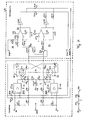
- the well-known complementary amplifier of Fig. 1 includes in series a npn transistor Q1 and a pnp transistor Q2 between two voltage terminals + Ub and -Ub, which are fed by two series-connected voltage sources V2, V3.
- the connection node of these voltage sources is connected to the ground potential GND and to a terminal of the load RL.
- the other terminal of this load RL is located at the connection node of the two transistors Q1, Q2.
- For the Closed-circuit current adjustment of the two transistors Q1, Q2 provides an adjustable bias source Vbias between the two bases of these transistors. By suitable adjustment of the bias voltage Vbias, the quiescent current of the two transistors can be adjusted so that they operate, for example, in each case in the AB amplification mode.
- the unbalanced input voltage is supplied via an input + in the base of the npn transistor.
- the complementary amplifier is noninverting with respect to the load terminal facing away from the mass.
- Capacitors for potential separation are in Fig. 1 not shown. In any case, they are necessary when a DC voltage is superimposed on the input signal and the input voltage swing is not very large with respect to the base-emitter voltage of transistor Q1.
- the well-known complementary amplifier after Fig. 2 unlike Fig. 1 only one voltage source V4 for the two series-connected complementary transistors Q3, Q4 of an NPN and a PNP transistor, which are located between a positive supply terminal + Ub and the ground terminal GND.
- the voltage source V4 is connected to ground GND with its one terminal and supplies the supply terminal + Ub with the other.
- the quiescent current setting for the two transistors is as in Fig. 1 via an adjustable bias source Vbias, which lies between the two base terminals. Since the common emitter terminal in this complementary circuit is also no longer approximately at the ground potential GND, there is a voltage difference between the common emitter terminal and the ground GND in the idle state, which corresponds approximately to half the supply voltage V4.
- the signal input + must also be separated in voltage by a capacitor from the signal source, since the signal input + approximately half the supply voltage V4 and thus generally differs greatly from the rest potential of the signal source.
- Fig. 3 shows the one already mentioned U.S. Patent US 4,229,706 described symmetric-structure audio-balanced power amplifier, which is DC-coupled in the two signal paths and whose two npn-output stage transistors Q1, Q2 are each fed by a floating power supply V1, V2.
- the galvanic separation of the ground reference potential GND is in the floating power supply usually by means of its own power transformer and a bridge rectifier circuit reached.
- the load RL is connected between the two emitters, which also form the bases for the cross-connected floating supply voltages V1, V2.
- the balanced input signal is fed via the inputs + in and -in, the positive input + in being connected to the non-inverting input of an operational amplifier U1 implemented in bipolar technology.
- the negative input -in is connected to the non-inverting input of a second operational amplifier U2 identical to the first operational amplifier U1.
- the output of the first and second operational amplifier is connected directly, ie without a coupling capacitor, to the base of the first and second output transistors Q1, Q2.
- the voltage supply of the two operational amplifiers via two series-connected voltage sources V3, V4, the node of which is connected to the ground potential GND and the mass-remote poles form the positive and negative supply voltage + V, -V for the two operational amplifiers U1, U2.
- the quiescent current setting of the two output transistors Q1, Q2 takes place in each case via a resistor R4 or R5 between the emitter and the negative supply voltage -V.
- the associated base current supplies the output of the associated operational amplifier U1 or U2. This presents a problem now, since the current determined by the resistor R4 or R5 must be identical to the base current supplied by the operational amplifier U1 or U2, since this current is only linked to the voltage sources V3, V4 and no other current path is available stands. So it is not regulated the emitter quiescent current, but the base current.
- the resulting emitter quiescent current which is essentially supplied by the floating voltage supply V1 or V2 and flows back via the load RL, is directly dependent on the current amplification factor of the respective output transistor Q1 or Q2 and diffuses therewith, which is actually undesirable.
- the current regulation strictly speaking the regulation of the base current, is effected by tapping off the respective emitter potential and returning it via a relatively high-resistance resistor R2 or R3 to the inverting input of the first or second operational amplifier U1, U2.
- both emitters which also form the connection points for the load RL, are as close as possible to the same potential
- these two circuit nodes are also connected to one another via a relatively high-resistance resistor R6 and thus the difference of the two potentials as a kind of offset voltage to the inverting Inputs of the operational amplifier U1, U2 returned.
- the relatively small quiescent current not the modulation of the Output transistors Q1, Q2 obstructed, increases the respective emitter current through a resistor diode path R7, D1 and R8, D2, which provides the respective emitter a lower resistance current path to ground GND available when the diode becomes conductive.
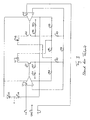
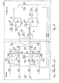
- Fig. 4 schematically shows the circuit diagram of a first embodiment of a balanced push-pull amplifier according to the invention.
- the two signal paths are constructed symmetrically and each contain a preamplifier block N1B or N2B and a power amplifier M1 or M2.
- the power amplifiers M1, M2 are each connected to a floating power supply V1, V2, wherein the load circuits via a load RL, which is connected between the bases of the two power amplifiers M1, M2, are cross-closed.
- the two base points of the power amplifiers also represent the connection points or terminals RL1, RL2 for the externally connected load RL and form the signal output.
- the voltage supply device of the preamplifier blocks N1B, N2B contains at least two series-connected voltage sources V3, V4 whose connection point is connected to ground GND.
- the resulting supply voltages + Ub and -Ub feed the supply terminals of the preamplifier blocks, which in the embodiment of Fig. 4 each consist of an input side amplifier N1, N2 with high open-loop gain.
- the positive pole of the output stage of the amplifiers N1, N2 is supplied with the positive supply voltage + Ub or with another positive and earth-related voltage source.
- the negative pole of the output stage of the amplifiers N1, N2 is connected via a potential difference generator 4, 5 to the associated load terminal RL1, RL2. About this potential difference generator 4, 5 flows an impressed current.
- the amplifiers N1, N2 Due to the high open-loop gain in conjunction with a high-impedance non-inverting and high-impedance inverting input, with negligible offset voltage and negligible offset current and with a low-impedance output, the amplifiers N1, N2 have a behavior like a more or less ideal operational amplifier.
- the first power amplifier M1 is powered by a floating first voltage source V1 and the second power amplifier M2 is powered by a floating second voltage source V2.
- the first power amplifier M1 is connected via its first supply terminal to one pole of the first voltage source V1 and via its second supply terminal, which also serves as a power amplifier output, to the first output RL1 and via the load RL to the other pole of the first voltage source V1.
- the second power amplifier M2 is connected via its first supply terminal to a pole of the second voltage source V2 and via its second supply terminal, which also serves as a power amplifier output, to the second output RL2 and via the load RL to the other pole of the second voltage source V2,
- the required operating point-determining control voltage is determined in the associated potential difference generators 4, 5 by a predetermined by a quiescent current setting Ix with an adjustable current source I1, which generates the desired potential offset via the potential difference generator 4, 5.
- the closed-circuit current setting device Ix connected to the negative supply connection -Ub contains an adjustable current source I1 whose current is split in half between the two potential difference generators 4, 5 by means of the two resistors R2, R3 connected to the output terminals RL1, RL2, so that the operating point setting for the two Power amplifier M1, M2 takes place symmetrically.
- a temperature-influenced control which, via a temperature sensor which detects the temperature of at least one power component, influences the adjustable current or voltage source I1 or Vbias such that the quiescent current of the power components of the power amplifiers M1, M2 remains constant or has a predetermined temperature profile
- a complete automatic control is such that the current quiescent current value of the power components of the power amplifiers M1, M2 is measured and compared with a predetermined setpoint and deviations occurring from the setpoint by automatically adjusting the quiescent current setting Ix away become.
- the two amplifiers N1 and N2 have an inverting and a non-inverting input and, because of their high open-loop gain, each correspond to an operational amplifier.
- the output of the resulting operational amplifier is most suitably the load connection RL1 or RL2, which is controlled by a feedback network to the ground potential GND.
- the feedback network is formed by the series-connected resistors R6 and R7 or R8 and R9, which are connected between the load terminal RL1 and ground GND and the load terminal RL2 and ground GND.
- the common connection point of the resistors R6, R7 and R8, R9 is connected to the inverting input of the amplifier N1 and N2, respectively.
- the non-inverting input of the first amplifier N1 is connected to the positive signal input + in and the non-inverting input of the second amplifier N2 is connected to the negative signal input -in of the push-pull amplifier.
- the feedback network R6, R7 and R8, R9 the output of the amplifier N1 or N2 is controlled so that the potential at the noninverting input of the amplifier N1 or N2 via the potential difference generator 4, 5 and the voltage divider R6, R7 and R8, R9 N2 is identical to the potential at the positive or negative signal input + in or -in.
- This regulation via the feedback network is independent of the magnitude of the quiescent current setting for the power components of the power amplifiers M1, M2, which is predetermined by the adjustable current source I1.
- the resulting level offset at the potential difference generator 4 or 5 is regulated by the amplifier N1 or N2.
- the resistors R10 and R11 from the positive and negative signal input to ground GND have no meaning for the feedback. They merely serve to determine the GND potential for the respective non-inverting inputs of N1 and N2 and the line adaptation, since the signal inputs at the non-inverting inputs of the amplifiers N1 and N2 are usually high-impedance.
- An embodiment is shown below in which the signal inputs are connected to the inverting inputs of the amplifiers N1 and N2. By connected to these inputs feedback network these inputs are then much lower impedance, so that a line adjustment may be omitted if necessary.
- the ratio of the resistors R6 / R7 and R8 / R9 determines the overall gain of the push-pull amplifier.
- the upper amplifier half consisting essentially of the modules N1B and M1, amplifies the one half-wave of the balanced input signal and the lower amplifier half, consisting of the modules N2B and M2, amplifies the other half-wave.
- the power amplifiers M1, M2 can be practically implemented in a variety of ways: as individual power devices such as power electronics. Power MOSFETs, IGBTs or bipolar power transistors, but also advantageous combinations of similar or different amplifier components with or without local negative feedback.
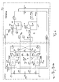
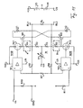
- the output stages of the preamplifier blocks N1B and N2B are exemplified as triode Xtr1 and Xtr2, respectively.
- the preamplifier blocks N1B and N2B thus each consist of the combination of an input-side amplifier N1, N2 with high open-loop gain and a connected to the amplifier N1, N2 tube Xtr1, Xtr2, the control grid is connected to the associated amplifier output.
- the anode of the tube Xtr1, Xtr2 is connected to the positive supply voltage + Ub or to another positive and also earth-related voltage source.
- the cathode of the tube Xtr1, Xtr2 is connected to the associated load terminal RL1, RL2 via a potential difference generator 4, 5 which in the simplest case contains a resistor R4, R5 and through which an impressed current flows.
- tetrodes pentodes, hexodes and heptodes can also be used as circuits of the additional gratings corresponding to the prior art as tubes Xtr1, Xtr2 shown as triodes.
- FIG. 5 show two n-channel MOSFETs whose respective gate electrode is connected to the cathode of the preceding tube Xtr1, Xtr2.
- the respective source electrode is connected to the associated load terminal RL1, RL2 and the respective drain electrode to the positive potential of floating voltage source V1, V2 connected.
- the operating point-determining gate-source control voltage is determined in the associated potential difference generators 4, 5 by a predetermined by a quiescent current setting Ix with an adjustable current source I1, which generates the desired potential offset via the resistors R4, R5.
- the quiescent current adjuster Ix connected to the negative supply terminal -Ub contains an adjustable current source I1 whose current is split in half by means of the two resistors R2, R3 connected to the output terminals RL1, RL2 to the two resistors R4, R5, so that the operating point setting for the two MOSFETs M1, M2 takes place symmetrically.
- the circuit block B1 includes two control circuits B2, B3 whose inputs are coupled to the amplifier outputs RL1, RL2 and their outputs to the feedback networks of the two preamplifier blocks N1B and N2B, respectively.
- the input of the first control circuit B2 is formed by two series-connected equal resistors R16, R17, which are connected to the outputs RL1, RL2 and the common connection point avg is connected via a resistor R15 to the inverting input of an operational amplifier U3.
- a DC voltage V5 is applied at the non-inverting input of U3 .
- the output of the amplifier U3 is fed back to the non-inverting input by means of a capacitor C2.
- the voltage supply of the amplifier U3 is expediently carried out via the already existing supply potentials + Ub and -Ub or via another supply voltage.
- the input of the second control loop B3 is formed by a subtractor D1, whose minimum input + to the load terminal RL2 and whose subtrahende input - to the load terminal RL1 is connected.
- the output of the subtracter D1 determines the potential of the node diff and is connected via a resistor R14 to the inverting input of an amplifier U4, which is connected via a capacitor C1 to its amplifier output.
- This output is further connected via a series circuit of an inverter N4 and a resistor R12 to the circuit node bias 1 and via a resistor R13 to the other circuit node bias 2.
- the ground potential GND is connected.
- the inventive function of the control block Biasregelung B1 is that by means of the first control loop B2 of the average avg of the potentials detected at the outputs RL1, RL2 and compared with a predetermined target voltage V5.
- the deviation of the potential avg from the desired value V5 is amplified via the integrator formed by the amplifier U3.
- this amplified deviation from the desired value V5 acts in the same way on the two directly coupled control interfaces bias 1 and bias 2, that the mean value of the potentials at the output terminals RL1, RL2 to the predetermined target value V5 is adjusted.
- the absolute value of the absolute value of the outputs RL1, RL2 is set defined.
- ⁇ 2 greater than or equal to 1s makes sense.
- the amplifiers N1 or N2 are implemented in the preamplifier blocks in such a way that a considerable drift-loaded potential difference between the non-inverting and inverting inputs of these amplifiers N1, N2 occurs at rest, this can have a disturbing influence on the Working point stability can be minimized.
- the first stage of a tube amplifier could be realized as a cathode base stage.
- the grid corresponds to the non-inverting input of the amplifier N1 or N2 and the cathode corresponds to the inverting input of N1 or N2.
- the cathode current results in a potential increase across the resistor R7 or R9.
- the operating points of tubes are subject to thermal and aging-related fluctuations.
- the current component I (R6) or I (R8) changes via the temperature and the aging of the input tubes, which essentially bring about the voltage amplification in the amplifiers N1 or N2, and thus according to the first relationship, that indicated by I (R4 ) certain potential of the gate-source path of the power amplifier M1.
- the potential determined by the current I (R5) has an effect on the gate-source path of the final amplifier M2.
- the setpoint voltage V5 is not fixed, but as in the exemplary embodiment of FIG Fig.
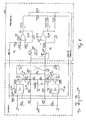
- control interfaces bias 1 and bias 2 are interconnected via the series-connected equal resistors R24 and R25, so that a new node voltage avgln for a third control loop B4 is available at the common resistor tap.
- This node voltage avgln is fed via a resistor R26 to the non-inverting input of the control amplifier U3, which is different than in Fig. 5 is not supplied with a reference voltage V5, but generates its reference voltage at this terminal itself by a capacitor C3 is connected there.
- the mean value of the potentials at the control interfaces bias 1 and bias 2 is thus low-pass filtered via the RC element R26 and C3 and then serves as a reference voltage at the noninverting input of the control amplifier U3.
- the corner frequency of the RC element R26, C3 is preferably chosen lower than the lowermost to be transmitted useful signal frequency at least a decade.
- the fundamental or drift-related potential difference between the inputs of the amplifiers N1 and N2, to which a portion of the output voltage is fed back via the negative feedback network, and the output nodes RL1 and RL2, respectively, are ideally regulated to zero or at least so small that the error component is thereby reduced the quiescent current control has no influence.
- Fig. 7 an embodiment of the push-pull amplifier is shown, which has as output amplifiers M1, M2 respectively tubes Xtr3, Xtr4, which directly drive the load RL.
- the preamplifier blocks N1B, N2B contain, in contrast to the preceding embodiments Fig. 5 and Fig. 6 no combination amplifier, but consist solely of the amplifiers N1, N2. These are realized so that they have a negative DC output voltage of several volts to several tens of volts depending on the connected tubes Xtr3, Xtr4 at rest.
- the adjustable current source I1 is connected to a positive potential + Ub, so that half its current flows via the resistors R2, R3, the level converters 4, 5 and the internal output stage from N1, N2 to the negative supply voltage -Ub.
- This current flow causes the required negative grid bias on the resistors R4, R5 for the tubes Xtr3 and Xtr4, respectively. It is thus again defined with only one manipulated variable of the quiescent current of both tubes Xtr3, Xtr4 in the floating without fixed ground reference driven amplifiers M1, M2 and set synchronously and symmetrically.
- the quiescent current of the tubes Xtr3, Xtr4 can be performed in a variety of ways manually, temperature-controlled or by means of an automatic quiescent current control loop.
- triodes were used.
- Xtr3, Xtr4 but all known tube types such as tetrodes and pentodes can be used.
- the load RL has to be coupled by means of a transformer to the tube-equipped power output stage M1, M2 in a special requirement, this can be done with the same structure as in FIG Fig. 7 take place, except that instead of the direct load coupling a transformer down-converted in a known manner, the internal resistance of the tube output stage to the low-impedance load.
- the transformer can be performed cost saving as autotransformer, since no Gleichstromvormagnetmaschine occurs by the quiescent current adjustment according to the invention.
- the autotransformer is wound symmetrically, for example in a two-chamber design, so that the same winding resistances result for both winding halves. Due to the lack of DC biasing, a realization as a toroidal transformer is also possible.
- the winding is in this case divided into integer equal parts, which are then wound in pairs bifilar.
- FIG. 8 Another embodiment of the push-pull amplifier according to the invention shows Fig. 8 , This circuit is almost identical to the circuit of Fig. 6 , except that the manipulated variable for the quiescent current setting is not as in Fig. 6 is carried out by the adjustable current source I1, but by an adjustable voltage source Vbias, but ultimately via the resistors R2, R3 also generates a current that is split in half by means of these resistors R2, R3 and the resistors R4, R5 the desired operating point determining potential offset for generates the respective gate-source path of the two n-channel MOSFETs in the power amplifier M1, M2.
- the absolute value of the potentials at the load terminals RL1, RL2 is defined and adjusted to an approximately equal value. Since the resistors R2 and R3 are equal to each other, the currents I (R2) and I (R3) flowing therethrough are also equal to each other. These currents flow almost completely through the resistors R4 and R5 and from the cathode to the anode of the triode Xtr1 and Xtr2 to the positive operating voltage + Ub. Due to the resulting potential offset at the resistors R4 and R5, a defined positive potential difference between the gate-source path of the MOSFETs M1 and M2 is generated, and consequently a defined quiescent current flows through these output stage transistors. The adjustment process of the voltage source Vbias can again take place in a variety of ways, manually, temperature-controlled or by means of an automatic quiescent current control loop.
- a push-pull amplifier according to the invention can also be realized in that the input-side amplifiers N1, N2 in the preamplifier blocks N1B, N2B are each connected with their inverting amplifier input to the signal inputs -in or + in the push-pull amplifier.
- the input area of the amplifiers N1, N2 only minor circuit changes have to be made.
- the resistors R7 and R9 of the feedback networks are now not connected to the ground potential as for example, in the comparable Fig. 5 but to the negative or positive signal input -in or + in the push-pull amplifier.
- the resistors R10 and R11 at the non-inverting inputs of the amplifiers N1 and N2 are connected at the ends remote from the amplifier to the ground potential GND. Furthermore, the recirculated lines of the rule interfaces bias 1 and bias 2 are no longer as in Figure 5 to the inverting input of the amplifier N1 or N2, but to their non-inverting inputs.
- the control currents fed back by the control circuits B2 and B3 generate the required control voltages for the amplifiers N1, N2 via the resistors R10 and R11, respectively.
- Fig. 10 shows a further variant of the quiescent current setting.
- the basic circuit of this push-pull amplifier is approximately comparable to the circuit of Fig. 5 ,
- the potential difference generators 4 and 5 each contain an optoelectronic component OK1 or OK2 or are coupled to such components.
- the light emission is controlled in each case an LED element, is dependent on the intensity of the volume resistivity of a photosensitive photo-transistor.
- This photo-transistor is parallel to that of already Fig. 5 known resistor R4 or R5, which is fed via the likewise known resistor R2 or R3, but its base point in contrast to Fig. 5 on the negative fixed potential -Ub.
- the potential difference generator 4 and 5 are thus formed by an assembly that combines the resistors R4 and R5 each with an opto-coupler distance OK1 and OK2 in itself.
- a synchronous adjustment of the quiescent current of both branches of the floating voltage-supplied power amplifier is carried out by the application of both optocouplers with the same control or regulating current.
- the current equality is in the exemplary embodiment after Fig. 10 thereby forced that the current of the adjustable current source I1 from the negative supply terminal -Ub is looped through both optocouplers OK1, OK2 to the positive supply terminal + Ub.
- the embodiment according to Fig. 11 shows an advantageous arrangement of the push-pull amplifier according to the invention, when in principle only unbalanced input signals to be processed instead of symmetrical input signals.
- the circuit is suitable for Fig. 5 , In order for both signal branches to be able to operate simultaneously, ie at each half-wave, the amplifier N1 at the non-inverting input and the amplifier N2 at the inverting input are driven.
- the non-inverting input of the amplifier N1 is connected to the signal input + in and via the resistor R10 to the ground potential GND.
- the inverting input of the amplifier N1 is as in Fig.
Claims (10)
- Amplificateur dans une version en push-pull symétrique comprenant un premier dispositif d'amplification et un second dispositif d'amplification identique au premier, le premier dispositif d'amplification (N1B, M1) étant raccordé dans un premier chemin de signal entre une première entrée (+in) et une première sortie (RL1), et un second dispositif d'amplification (N2B, M2) étant raccordé dans un second chemin de signal entre une seconde entrée (-in) et une seconde sortie (RL2), et également un signal à amplifier peut être raccordé à la première et/ou à la seconde entrée (+in, -in) et une charge (RL) à raccorder de façon externe peut être raccordée à la première et à la seconde sorties (RL1, RL2),- la première entrée (+in) est couplée avec l'entrée de signal d'un premier bloc préamplificateur (N1B) alimenté par un dispositif d'alimentation en tension (V3, V4) et sa sortie est couplée avec l'entrée de signal d'un premier amplificateur final (M1), et la seconde entrée (-in) est couplée avec l'entrée de signal d'un second bloc préamplificateur (N2B) alimenté par le dispositif d'alimentation en tension (V3, V4) et sa sortie est couplée avec l'entrée de signal d'un second amplificateur final (M2),- le premier amplificateur final (M1) est alimenté par une première source de tension (V1) flottante et le second amplificateur final (M2) est alimenté par une seconde source de tension (V2) flottante,- le premier amplificateur final (M1) est relié par son premier branchement d'alimentation à un pôle de la première source de tension (V1) et par son second branchement d'alimentation, qui sert également de sortie d'amplificateur final, à la première sortie (RL1) et par la charge (RL) à l'autre pôle de la première source de tension (V1), et- le second amplificateur final (M2) est relié par son premier branchement d'alimentation à un pôle de la seconde source de tension (V2) et par son second branchement d'alimentation, qui sert également de sortie d'amplificateur final, à la seconde sortie (RL2) et par la charge (RL) à l'autre pôle de la seconde source de tension (V2),caractérisé en ce que,- un premier générateur de différence de potentiel (4) entre la sortie du premier bloc préamplificateur (N1B) et la première sortie (RL1) génère en fonction d'un dispositif de réglage de courant de repos (lx) une première tension différentielle entre la sortie du premier bloc préamplificateur (N1B) et la première sortie (RL1), qui détermine le point de travail et le courant de repos du premier amplificateur final (M1), et- un second générateur de différence de potentiel (5) entre la sortie du second bloc préamplificateur (N2B) et la seconde sortie (RL2) génère en fonction du dispositif de réglage de courant de repos (lx) une seconde tension différentielle entre la sortie du second bloc préamplificateur (N2B) et la seconde sortie (RL2), qui règle le point de travail et le courant de repos du second amplificateur final (M2).
- Amplificateur selon la revendication 1, caractérisé en ce que le premier et le second bloc préamplificateur (N1B, N2B) contiennent des tubes et/ou des semi-conducteurs et l'adaptation de tension côté sortie au premier et au second amplificateur final (M1, M2) s'effectue au moyen du premier et du second générateurs de différence de potentiel (4, 5) attribués en liaison avec le dispositif de réglage du courant de repos (lx).
- Amplificateur selon la revendication 2, caractérisé en ce que, en supplément du premier et du second bloc amplificateur (N1B, N2B), un dispositif de réglage (B1) amène en fonction des tensions de décalage sur la première et la seconde sortie (RL1, RL2) des signaux de correction (bias2, bias1) au premier et/ou au second bloc amplificateur (N1B, N2B) et élimine ou tout au moins réduit ainsi des tensions de décalage sur la première et la seconde sortie (RL1, RL2).
- Amplificateur selon la revendication 3, caractérisé en ce que le dispositif de réglage (B1) contient une première unité de réglage (B2) à laquelle sont amenés comme valeur réelle un signal (avg) dépendant des points de travail de tension continue de la première et de la seconde sortie (RL1, RL2) et comme valeur prescrite un niveau de tension continu prédéfini (V5).
- Amplificateur selon la revendication 3 ou 4, caractérisé en ce que le dispositif de réglage (B1) contient une seconde unité de réglage (B3) , à laquelle est amenée comme valeur réelle la différence de tension (diff) entre la première sortie et la seconde sortie (RL1, RL2), la valeur zéro de différence de tension servant de valeur prescrite.
- Amplificateur selon la revendication 5, caractérisé en ce que le dispositif de réglage (B1) contient une troisième unité de réglage (B4), de sorte que le niveau de tension continue prédéfini est formé au moyen d'un dispositif de filtre à partir de la valeur moyenne de potentiel de la première et de la seconde entrée (+in, - in).
- Amplificateur selon la revendication 5, caractérisé en ce que le niveau de tension continue prédéfini pour la première unité de réglage (B2) est formé au moyen d'un dispositif de filtre (R26, C3) à partir de la valeur moyenne de potentiel (avgin) des entrées respectives du premier et du second bloc préamplificateur (N1B, N2B) qui sont reliées chacune au moyen d'un réseau de contre-couplage à la première ou à la seconde sortie (RL1, RL2).
- Préamplificateur selon au moins une quelconque des revendications 1 à 7, caractérisé en ce que le dispositif de réglage du courant de repos (lx) règle le courant de repos pour le premier et le second préamplificateur final (M1, M2) au moyen d'une valeur de commande dépendante de la température, la température étant déterminée en particulier dans la zone des amplificateurs finals.
- Amplificateur selon au moins l'une quelconque des revendications 1 à 7, caractérisé en ce que le dispositif de réglage du courant de repos (lx) contient un régulateur qui mesure la valeur réelle du courant de repos d'au moins un amplificateur final (M1, M2) et la règle ultérieurement sur une valeur prescrite.
- Amplificateur selon au moins l'une quelconque des revendications 1 à 8, caractérisé en ce que des contre-couplages locaux et/ou des mesurés de compensation servent dans les deux chemins de signal à l'amélioration du comportement linéaire à la transmission.
Applications Claiming Priority (2)
| Application Number | Priority Date | Filing Date | Title |
|---|---|---|---|
| DE10360347A DE10360347A1 (de) | 2003-12-22 | 2003-12-22 | Symmetrischer Gegentaktverstärker |
| DE10360347 | 2003-12-22 |
Publications (2)
| Publication Number | Publication Date |
|---|---|
| EP1548934A1 EP1548934A1 (fr) | 2005-06-29 |
| EP1548934B1 true EP1548934B1 (fr) | 2008-09-03 |
Family
ID=34530345
Family Applications (1)
| Application Number | Title | Priority Date | Filing Date |
|---|---|---|---|
| EP04030390A Not-in-force EP1548934B1 (fr) | 2003-12-22 | 2004-12-22 | Amplificateur push-pull totalement différentiel |
Country Status (3)
| Country | Link |
|---|---|
| EP (1) | EP1548934B1 (fr) |
| AT (1) | ATE407478T1 (fr) |
| DE (2) | DE10360347A1 (fr) |
Cited By (1)
| Publication number | Priority date | Publication date | Assignee | Title |
|---|---|---|---|---|
| US10320343B1 (en) | 2018-03-08 | 2019-06-11 | Real Analog, Llc | Amplifier output stage using toroidal transformer |
Families Citing this family (1)
| Publication number | Priority date | Publication date | Assignee | Title |
|---|---|---|---|---|
| DE102008025347B4 (de) * | 2007-12-22 | 2015-07-09 | Klaus Zametzky | Elektronischer Verstärker |
Family Cites Families (7)
| Publication number | Priority date | Publication date | Assignee | Title |
|---|---|---|---|---|
| US4229706A (en) * | 1979-01-05 | 1980-10-21 | Bongiorno James W | Audio amplifier |
| GB2113495B (en) * | 1981-11-10 | 1985-02-27 | Whitmore Adkin F | Low supply voltage amplifier |
| FR2547470A1 (fr) * | 1983-06-08 | 1984-12-14 | Scherer Rene | Regulateur de courant de polarisation pour amplificateurs a symetrie complementaire et etages de sortie utilisant ce regulateur |
| US4719431A (en) * | 1986-04-21 | 1988-01-12 | Karsten Ralph R | Audio power amplifier |
| JPH10506506A (ja) * | 1994-07-13 | 1998-06-23 | ビー・エイチ・シー コンサルティング ピー・ティー・ワイ リミテッド | 改良増幅器 |
| WO2000011779A1 (fr) * | 1998-08-19 | 2000-03-02 | Ryszard Parosa | Circuit pour la detection et la regulation precises de courant de repos continu dans des amplificateurs de puissance a transistors |
| US6242977B1 (en) * | 1999-05-26 | 2001-06-05 | Atma-Sphere Music Systems, Inc. | Amplifier and preamplifier circuit |
-
2003
- 2003-12-22 DE DE10360347A patent/DE10360347A1/de not_active Withdrawn
-
2004
- 2004-12-22 AT AT04030390T patent/ATE407478T1/de active
- 2004-12-22 DE DE502004007977T patent/DE502004007977D1/de active Active
- 2004-12-22 EP EP04030390A patent/EP1548934B1/fr not_active Not-in-force
Cited By (2)
| Publication number | Priority date | Publication date | Assignee | Title |
|---|---|---|---|---|
| US10320343B1 (en) | 2018-03-08 | 2019-06-11 | Real Analog, Llc | Amplifier output stage using toroidal transformer |
| US10707816B2 (en) | 2018-03-08 | 2020-07-07 | Real Analog, Llc | Amplifier output stage using toroidal transformer |
Also Published As
| Publication number | Publication date |
|---|---|
| ATE407478T1 (de) | 2008-09-15 |
| DE502004007977D1 (de) | 2008-10-16 |
| EP1548934A1 (fr) | 2005-06-29 |
| DE10360347A1 (de) | 2005-07-21 |
Similar Documents
| Publication | Publication Date | Title |
|---|---|---|
| DE112012000470T5 (de) | Vorrichtung und Verfahren zur Miller-Kompensation bei mehrstufigen Verstärkern | |
| DE112017001304T5 (de) | Aktive Linearisierung für Breitbandverstärker | |
| DE3035272A1 (de) | Operations-transkonduktanzverstaerker mit einer nichtlineare komponente aufweisenden stromverstaerkern | |
| DE2947771C2 (de) | Direkt gekoppelte Verstärkeranordnung mit Stabilisierung des Ausgangsgleichstroms | |
| DE3432510C2 (fr) | ||
| DE3832448A1 (de) | Messverstaerker mit programmierbarer verstaerkung | |
| WO1992019040A1 (fr) | Circuit de transducteur | |
| EP1310043B1 (fr) | Amplificateur differentiel complementaire | |
| DE3011835A1 (de) | Leistungsverstaerker | |
| DE4122057A1 (de) | Rueckkopplungssteuerung zur verringerung der durch eine differenzverstaerkerstufe hervorgerufenen signalverzerrung | |
| EP0290080B1 (fr) | Circuit d'amplification d'un signal de télévision | |
| WO2018215030A1 (fr) | Circuit à amplificateur à transimpédance | |
| DE102013109957B4 (de) | Schaltung zum Verhindern von lastinduzierter Nichtlinearität in Operationsverstärkern | |
| DE10351593B4 (de) | Integrierte Vorverstärkerschaltung für die Erfassung eines Signalstroms von einer Photodiode | |
| EP1548934B1 (fr) | Amplificateur push-pull totalement différentiel | |
| DE102014003232B4 (de) | Hocheffiziente ultra-lineare A-Klasse-Ausgangsstufe | |
| DE3448087C2 (fr) | ||
| DE3007715C2 (fr) | ||
| DE102006034560B4 (de) | Verstärkerstufe, Operationsverstärker und Verfahren zur Signalverstärkung | |
| DE19962811B4 (de) | Gegentaktverstärkerschaltung | |
| DE102008025347B4 (de) | Elektronischer Verstärker | |
| EP1101279A1 (fr) | Etage de sortie d'amplificateur | |
| DE4320061C1 (de) | Verstärkerausgangsstufe | |
| DE2951161A1 (de) | Verstaerker | |
| DE3305482A1 (de) | Durch vormagnetisierungsstrom kompensierter verstaerker |
Legal Events
| Date | Code | Title | Description |
|---|---|---|---|
| PUAI | Public reference made under article 153(3) epc to a published international application that has entered the european phase |
Free format text: ORIGINAL CODE: 0009012 |
|
| AK | Designated contracting states |
Kind code of ref document: A1 Designated state(s): AT BE BG CH CY CZ DE DK EE ES FI FR GB GR HU IE IS IT LI LT LU MC NL PL PT RO SE SI SK TR |
|
| AX | Request for extension of the european patent |
Extension state: AL BA HR LV MK YU |
|
| 17P | Request for examination filed |
Effective date: 20051223 |
|
| AKX | Designation fees paid |
Designated state(s): AT BE BG CH CY CZ DE DK EE ES FI FR GB GR HU IE IS IT LI LT LU MC NL PL PT RO SE SI SK TR |
|
| 17Q | First examination report despatched |
Effective date: 20061211 |
|
| GRAP | Despatch of communication of intention to grant a patent |
Free format text: ORIGINAL CODE: EPIDOSNIGR1 |
|
| GRAS | Grant fee paid |
Free format text: ORIGINAL CODE: EPIDOSNIGR3 |
|
| GRAA | (expected) grant |
Free format text: ORIGINAL CODE: 0009210 |
|
| AK | Designated contracting states |
Kind code of ref document: B1 Designated state(s): AT BE BG CH CY CZ DE DK EE ES FI FR GB GR HU IE IS IT LI LT LU MC NL PL PT RO SE SI SK TR |
|
| REG | Reference to a national code |
Ref country code: GB Ref legal event code: FG4D Free format text: NOT ENGLISH |
|
| REG | Reference to a national code |
Ref country code: CH Ref legal event code: EP |
|
| REG | Reference to a national code |
Ref country code: IE Ref legal event code: FG4D Free format text: LANGUAGE OF EP DOCUMENT: GERMAN |
|
| REF | Corresponds to: |
Ref document number: 502004007977 Country of ref document: DE Date of ref document: 20081016 Kind code of ref document: P |
|
| PG25 | Lapsed in a contracting state [announced via postgrant information from national office to epo] |
Ref country code: LT Free format text: LAPSE BECAUSE OF FAILURE TO SUBMIT A TRANSLATION OF THE DESCRIPTION OR TO PAY THE FEE WITHIN THE PRESCRIBED TIME-LIMIT Effective date: 20080903 Ref country code: NL Free format text: LAPSE BECAUSE OF FAILURE TO SUBMIT A TRANSLATION OF THE DESCRIPTION OR TO PAY THE FEE WITHIN THE PRESCRIBED TIME-LIMIT Effective date: 20080903 Ref country code: ES Free format text: LAPSE BECAUSE OF FAILURE TO SUBMIT A TRANSLATION OF THE DESCRIPTION OR TO PAY THE FEE WITHIN THE PRESCRIBED TIME-LIMIT Effective date: 20081214 |
|
| PG25 | Lapsed in a contracting state [announced via postgrant information from national office to epo] |
Ref country code: FI Free format text: LAPSE BECAUSE OF FAILURE TO SUBMIT A TRANSLATION OF THE DESCRIPTION OR TO PAY THE FEE WITHIN THE PRESCRIBED TIME-LIMIT Effective date: 20080903 Ref country code: SI Free format text: LAPSE BECAUSE OF FAILURE TO SUBMIT A TRANSLATION OF THE DESCRIPTION OR TO PAY THE FEE WITHIN THE PRESCRIBED TIME-LIMIT Effective date: 20080903 |
|
| NLV1 | Nl: lapsed or annulled due to failure to fulfill the requirements of art. 29p and 29m of the patents act | ||
| REG | Reference to a national code |
Ref country code: IE Ref legal event code: FD4D |
|
| PG25 | Lapsed in a contracting state [announced via postgrant information from national office to epo] |
Ref country code: BG Free format text: LAPSE BECAUSE OF FAILURE TO SUBMIT A TRANSLATION OF THE DESCRIPTION OR TO PAY THE FEE WITHIN THE PRESCRIBED TIME-LIMIT Effective date: 20081203 Ref country code: IE Free format text: LAPSE BECAUSE OF FAILURE TO SUBMIT A TRANSLATION OF THE DESCRIPTION OR TO PAY THE FEE WITHIN THE PRESCRIBED TIME-LIMIT Effective date: 20080903 |
|
| PG25 | Lapsed in a contracting state [announced via postgrant information from national office to epo] |
Ref country code: RO Free format text: LAPSE BECAUSE OF FAILURE TO SUBMIT A TRANSLATION OF THE DESCRIPTION OR TO PAY THE FEE WITHIN THE PRESCRIBED TIME-LIMIT Effective date: 20080903 Ref country code: SK Free format text: LAPSE BECAUSE OF FAILURE TO SUBMIT A TRANSLATION OF THE DESCRIPTION OR TO PAY THE FEE WITHIN THE PRESCRIBED TIME-LIMIT Effective date: 20080903 Ref country code: CZ Free format text: LAPSE BECAUSE OF FAILURE TO SUBMIT A TRANSLATION OF THE DESCRIPTION OR TO PAY THE FEE WITHIN THE PRESCRIBED TIME-LIMIT Effective date: 20080903 Ref country code: IS Free format text: LAPSE BECAUSE OF FAILURE TO SUBMIT A TRANSLATION OF THE DESCRIPTION OR TO PAY THE FEE WITHIN THE PRESCRIBED TIME-LIMIT Effective date: 20090103 Ref country code: PT Free format text: LAPSE BECAUSE OF FAILURE TO SUBMIT A TRANSLATION OF THE DESCRIPTION OR TO PAY THE FEE WITHIN THE PRESCRIBED TIME-LIMIT Effective date: 20090203 |
|
| BERE | Be: lapsed |
Owner name: BLOHBAUM, FRANK Effective date: 20081231 |
|
| PLBE | No opposition filed within time limit |
Free format text: ORIGINAL CODE: 0009261 |
|
| STAA | Information on the status of an ep patent application or granted ep patent |
Free format text: STATUS: NO OPPOSITION FILED WITHIN TIME LIMIT |
|
| PG25 | Lapsed in a contracting state [announced via postgrant information from national office to epo] |
Ref country code: MC Free format text: LAPSE BECAUSE OF NON-PAYMENT OF DUE FEES Effective date: 20081231 Ref country code: EE Free format text: LAPSE BECAUSE OF FAILURE TO SUBMIT A TRANSLATION OF THE DESCRIPTION OR TO PAY THE FEE WITHIN THE PRESCRIBED TIME-LIMIT Effective date: 20080903 Ref country code: DK Free format text: LAPSE BECAUSE OF FAILURE TO SUBMIT A TRANSLATION OF THE DESCRIPTION OR TO PAY THE FEE WITHIN THE PRESCRIBED TIME-LIMIT Effective date: 20080903 |
|
| 26N | No opposition filed |
Effective date: 20090604 |
|
| PG25 | Lapsed in a contracting state [announced via postgrant information from national office to epo] |
Ref country code: IT Free format text: LAPSE BECAUSE OF FAILURE TO SUBMIT A TRANSLATION OF THE DESCRIPTION OR TO PAY THE FEE WITHIN THE PRESCRIBED TIME-LIMIT Effective date: 20080903 |
|
| PG25 | Lapsed in a contracting state [announced via postgrant information from national office to epo] |
Ref country code: BE Free format text: LAPSE BECAUSE OF NON-PAYMENT OF DUE FEES Effective date: 20081231 |
|
| PG25 | Lapsed in a contracting state [announced via postgrant information from national office to epo] |
Ref country code: SE Free format text: LAPSE BECAUSE OF FAILURE TO SUBMIT A TRANSLATION OF THE DESCRIPTION OR TO PAY THE FEE WITHIN THE PRESCRIBED TIME-LIMIT Effective date: 20081203 |
|
| PGFP | Annual fee paid to national office [announced via postgrant information from national office to epo] |
Ref country code: FR Payment date: 20100107 Year of fee payment: 6 |
|
| PG25 | Lapsed in a contracting state [announced via postgrant information from national office to epo] |
Ref country code: PL Free format text: LAPSE BECAUSE OF FAILURE TO SUBMIT A TRANSLATION OF THE DESCRIPTION OR TO PAY THE FEE WITHIN THE PRESCRIBED TIME-LIMIT Effective date: 20080903 |
|
| PG25 | Lapsed in a contracting state [announced via postgrant information from national office to epo] |
Ref country code: LU Free format text: LAPSE BECAUSE OF NON-PAYMENT OF DUE FEES Effective date: 20081222 Ref country code: HU Free format text: LAPSE BECAUSE OF FAILURE TO SUBMIT A TRANSLATION OF THE DESCRIPTION OR TO PAY THE FEE WITHIN THE PRESCRIBED TIME-LIMIT Effective date: 20090304 Ref country code: CY Free format text: LAPSE BECAUSE OF FAILURE TO SUBMIT A TRANSLATION OF THE DESCRIPTION OR TO PAY THE FEE WITHIN THE PRESCRIBED TIME-LIMIT Effective date: 20080903 |
|
| PG25 | Lapsed in a contracting state [announced via postgrant information from national office to epo] |
Ref country code: TR Free format text: LAPSE BECAUSE OF FAILURE TO SUBMIT A TRANSLATION OF THE DESCRIPTION OR TO PAY THE FEE WITHIN THE PRESCRIBED TIME-LIMIT Effective date: 20080903 |
|
| PG25 | Lapsed in a contracting state [announced via postgrant information from national office to epo] |
Ref country code: GR Free format text: LAPSE BECAUSE OF FAILURE TO SUBMIT A TRANSLATION OF THE DESCRIPTION OR TO PAY THE FEE WITHIN THE PRESCRIBED TIME-LIMIT Effective date: 20081204 |
|
| PGFP | Annual fee paid to national office [announced via postgrant information from national office to epo] |
Ref country code: CH Payment date: 20110315 Year of fee payment: 7 |
|
| PGFP | Annual fee paid to national office [announced via postgrant information from national office to epo] |
Ref country code: GB Payment date: 20110114 Year of fee payment: 7 |
|
| REG | Reference to a national code |
Ref country code: FR Ref legal event code: ST Effective date: 20110831 |
|
| PG25 | Lapsed in a contracting state [announced via postgrant information from national office to epo] |
Ref country code: FR Free format text: LAPSE BECAUSE OF NON-PAYMENT OF DUE FEES Effective date: 20110103 |
|
| REG | Reference to a national code |
Ref country code: CH Ref legal event code: PL |
|
| GBPC | Gb: european patent ceased through non-payment of renewal fee |
Effective date: 20111222 |
|
| PG25 | Lapsed in a contracting state [announced via postgrant information from national office to epo] |
Ref country code: GB Free format text: LAPSE BECAUSE OF NON-PAYMENT OF DUE FEES Effective date: 20111222 Ref country code: CH Free format text: LAPSE BECAUSE OF NON-PAYMENT OF DUE FEES Effective date: 20111231 Ref country code: LI Free format text: LAPSE BECAUSE OF NON-PAYMENT OF DUE FEES Effective date: 20111231 |
|
| PGFP | Annual fee paid to national office [announced via postgrant information from national office to epo] |
Ref country code: AT Payment date: 20121228 Year of fee payment: 9 |
|
| PGFP | Annual fee paid to national office [announced via postgrant information from national office to epo] |
Ref country code: DE Payment date: 20131230 Year of fee payment: 10 |
|
| REG | Reference to a national code |
Ref country code: AT Ref legal event code: MM01 Ref document number: 407478 Country of ref document: AT Kind code of ref document: T Effective date: 20131222 |
|
| PG25 | Lapsed in a contracting state [announced via postgrant information from national office to epo] |
Ref country code: AT Free format text: LAPSE BECAUSE OF NON-PAYMENT OF DUE FEES Effective date: 20131222 |
|
| REG | Reference to a national code |
Ref country code: DE Ref legal event code: R119 Ref document number: 502004007977 Country of ref document: DE |
|
| PG25 | Lapsed in a contracting state [announced via postgrant information from national office to epo] |
Ref country code: DE Free format text: LAPSE BECAUSE OF NON-PAYMENT OF DUE FEES Effective date: 20150701 |