EP1548934B1 - Fully differential push-pull amplifier - Google Patents
Fully differential push-pull amplifier Download PDFInfo
- Publication number
- EP1548934B1 EP1548934B1 EP04030390A EP04030390A EP1548934B1 EP 1548934 B1 EP1548934 B1 EP 1548934B1 EP 04030390 A EP04030390 A EP 04030390A EP 04030390 A EP04030390 A EP 04030390A EP 1548934 B1 EP1548934 B1 EP 1548934B1
- Authority
- EP
- European Patent Office
- Prior art keywords
- amplifier
- output
- voltage
- input
- quiescent current
- Prior art date
- Legal status (The legal status is an assumption and is not a legal conclusion. Google has not performed a legal analysis and makes no representation as to the accuracy of the status listed.)
- Not-in-force
Links
Images


Classifications
-
- H—ELECTRICITY
- H03—ELECTRONIC CIRCUITRY
- H03F—AMPLIFIERS
- H03F3/00—Amplifiers with only discharge tubes or only semiconductor devices as amplifying elements
- H03F3/45—Differential amplifiers
- H03F3/45071—Differential amplifiers with semiconductor devices only
- H03F3/45076—Differential amplifiers with semiconductor devices only characterised by the way of implementation of the active amplifying circuit in the differential amplifier
- H03F3/45475—Differential amplifiers with semiconductor devices only characterised by the way of implementation of the active amplifying circuit in the differential amplifier using IC blocks as the active amplifying circuit
-
- H—ELECTRICITY
- H03—ELECTRONIC CIRCUITRY
- H03F—AMPLIFIERS
- H03F1/00—Details of amplifiers with only discharge tubes, only semiconductor devices or only unspecified devices as amplifying elements
- H03F1/32—Modifications of amplifiers to reduce non-linear distortion
- H03F1/3217—Modifications of amplifiers to reduce non-linear distortion in single ended push-pull amplifiers
-
- H—ELECTRICITY
- H03—ELECTRONIC CIRCUITRY
- H03F—AMPLIFIERS
- H03F3/00—Amplifiers with only discharge tubes or only semiconductor devices as amplifying elements
- H03F3/26—Push-pull amplifiers; Phase-splitters therefor
- H03F3/265—Push-pull amplifiers; Phase-splitters therefor with field-effect transistors only
-
- H—ELECTRICITY
- H03—ELECTRONIC CIRCUITRY
- H03F—AMPLIFIERS
- H03F5/00—Amplifiers with both discharge tubes and semiconductor devices as amplifying elements
-
- H—ELECTRICITY
- H03—ELECTRONIC CIRCUITRY
- H03F—AMPLIFIERS
- H03F2200/00—Indexing scheme relating to amplifiers
- H03F2200/411—Indexing scheme relating to amplifiers the output amplifying stage of an amplifier comprising two power stages
-
- H—ELECTRICITY
- H03—ELECTRONIC CIRCUITRY
- H03F—AMPLIFIERS
- H03F2203/00—Indexing scheme relating to amplifiers with only discharge tubes or only semiconductor devices as amplifying elements covered by H03F3/00
- H03F2203/45—Indexing scheme relating to differential amplifiers
- H03F2203/45134—Indexing scheme relating to differential amplifiers the whole differential amplifier together with other coupled stages being fully differential realised
-
- H—ELECTRICITY
- H03—ELECTRONIC CIRCUITRY
- H03F—AMPLIFIERS
- H03F2203/00—Indexing scheme relating to amplifiers with only discharge tubes or only semiconductor devices as amplifying elements covered by H03F3/00
- H03F2203/45—Indexing scheme relating to differential amplifiers
- H03F2203/45138—Two or more differential amplifiers in IC-block form are combined, e.g. measuring amplifiers
Definitions
- the essential quality criteria for power amplifiers are the lowest possible total harmonic distortion, a high bandwidth, the lowest possible internal resistance, the lowest possible transient intermodulation distortion and a high operating point stability of the power components.
- Power amplifiers can be constructed with very different active devices, the characteristics of which usually determine the structure of the amplifier: tubes of different construction, e.g. Triodes, tetrodes, pentodes, or semiconductor devices, e.g. Bipolar transistors, field effect transistors, MOSFETs and IGBTs. Tubes usually have a comparatively high internal resistance for use as power amplifiers and therefore have to be adapted to the low impedance of the loudspeaker with the aid of specially constructed transformers, the transformers. However, these transmitters limit the achievable bandwidth and are themselves the source of significant nonlinear distortions. The therefore desirable direct coupling of the usually low-impedance load of the loudspeaker requires the use of active components with the lowest possible internal resistance or the greatest possible steepness. For this reason, the use of semiconductor components such as bipolar transistors, MOSFETs or, more rarely, IGBTs has prevailed as state of the art.
- tubes of different construction e.g. Triodes, tetrodes, pentodes, or semiconductor devices,
- amplifiers with higher power requirements than complementary push-pull amplifiers are realized, with complementary bipolar transistors (npn and pnp transistor) or complementary MOSFETs (n-channel and p-channel transistor) or complementary IGBTs (n-channel and p-channel Type) with a bipolar or unipolar operating voltage source related to ground potential.
- complementary bipolar transistors npn and pnp transistor
- complementary MOSFETs n-channel and p-channel transistor
- complementary IGBTs n-channel and p-channel Type
- the illustrated principle of a typical solid-state push-pull amplifier or a corresponding push-pull output stage is the use of a complementary transistor pair.
- an adjustable bias voltage source To adjust the quiescent current through the complementary transistor pair is an adjustable bias voltage source, the lies between the two base terminals of the complementary transistor pair. The other circuit parts are then different from each other.
- Fig. 1 In the basic circuit of Fig. 1 are used in the power unit at least two series-connected voltage sources whose connection point is connected to ground, so that there is a positive and a negative supply voltage relative to the ground potential.
- the drive signal is a symmetrical signal related to ground potential.
- the load eg the loudspeaker, lies between the connection point of the complementary transistor pair and the ground connection.
- the drive signal is a ground potential related unipolar signal.
- the load When the load has a DC path, it must be capacitively separated from the output level terminals at different levels formed by the connection point of the complementary transistor pair and the ground terminal.
- tubes only control a negative current according to the electron flow between the cathode and the anode, so that an amplifier element that is complementary to the electron tube is missing.
- tubes can be operated very low distortion because of their square current-voltage characteristic.
- Optimal would be the combination of tubes as a voltage amplifier with fructsteil semiconductor devices, such as bipolar transistors, MOSFETs or IGBTs, as output side power amplifier.
- Of great advantage here would be a DC coupling between the individual gain stages, so that otherwise required for the potential separation coupling or bypass capacitors or transformers have no harmful effect on the frequency response or harmonic distortion.
- amplifiers with hybrid component assembly are known, which contain separately after tube or transistor use optimized pre and power amplifiers, which are usually capacitively coupled together.
- a problem in the search for the most symmetrical pair of complementary transistors is the very limited choice of pnp bipolar transistors, p-channel MOSFETs and p-channel IGBTs for high quality power amplifiers. This problem is not resolved by the construction of a quasi-complementary power level, but shifted at the expense of symmetry only in the driver stage.
- the pairs of complementary transistors which can be used in reality are by no means real pairs on closer analysis.
- the complementary transistors of a complementary pair differ substantially in terms of the magnitude of the current amplification factor in the case of bipolar transistors and the transconductance in MOSFETs and IGBTs. This is a major cause of nonlinearities in amplifier performance.
- the chip size of p-channel MOSFETs is approximately three times greater than the chip area of the complementary n-channel MOSFET. This inevitably leads to significantly different capacities, in particular the gate-source capacitance and the drain-source capacitance.
- the operating point of the power stage is in these tube circuits by means of a fixed grid bias voltage such as in U.S. Patent 4,719,431 or adjusted by a respective cathode resistor.
- the associated precursor or the voltage amplifier is capacitively coupled. Examples of this are shown in the US patents US 4,719,431 in Figure 4 and US 6,242,977 B1 in Fig.2 , DC coupling according to the prior art is possible only indirectly by means of a high-impedance voltage divider, which in turn must be bridged capacitively. Without this bypass capacitor, the AC voltage drop would be much too large.
- a direct DC coupling would further destabilize the already highly drift end point of the end tube or the parallel connected end tubes, since then the drift of the tube multiplied by the DC amplification factor of the end tube (s) would additionally affect.
- the type of quiescent current setting implemented works exclusively with bipolar transistors, since the level of the base current (current flow of the base-emitter path) is controlled via the driver and the resistor network.
- the exclusive bias current setting via the base current control works in cross coupled amplifiers only using ideally identical bipolar power transistors. In reality, the inevitable dispersion of the current gain factor will result in absolute and temperature dependent deviations between the quiescent currents of the two power transistors. This creates an unacceptably high differential leakage current through the load resistance of the connected loudspeaker.
- the operating point of the MOSFETs is by means of a fixed gate voltage via a voltage divider on the one hand (see. Fig. 4 Node 276, resistors 308 and 310) and a control voltage (from regulator 268) on the other hand.
- the temperature-dependent change of the drain current at constant gate-source voltage leads in the worst case to a significant change in the absolute value of the drain current and can lead to the worst case thermal destruction of the MOSFET.
- the set DC gate voltage must be from the output potential of the always upstream but in none of the US 6,242,977 B1 illustrated embodiments are electrically isolated by means of a capacitor. Thus, the desirable realization of a DC-coupled amplifier without coupling and / or bypass capacitors is not possible.
- the object of the invention is to provide an improved push-pull amplifier, which has a fully symmetrical design with functional units of the same conductivity type, allows the greatest possible freedom for the use of tubes and / or semiconductors and / or monolithic integrated circuits, allows a transformerless connection of the load and coupling to coupling and bypass capacitors and transformers omitted.
- the object is achieved by the features of claim 1.
- the advantages of the invention are that the proposed improvements a power amplifier with very high linearity, which preferably serves as an audio amplifier of the highest quality category is realized.
- the operating points can be adjusted in a simple manner, wherein remaining asymmetries of the functional units can be safely stabilized via additional control devices.
- the control devices can also be designed so that they can compensate for changes due to drift and temperature. Due to the required flexibility, the most suitable components can be used and combined with one another for the preamplifier blocks and the power amplifiers. Whether the power amplifier is basically driven by a balanced differential signal around the ground reference level or whether the differential signal is superimposed on a DC level or whether a unipolar drive signal is present, requires at most slight changes in the two signal paths or in the control devices.
- the well-known complementary amplifier of Fig. 1 includes in series a npn transistor Q1 and a pnp transistor Q2 between two voltage terminals + Ub and -Ub, which are fed by two series-connected voltage sources V2, V3.
- the connection node of these voltage sources is connected to the ground potential GND and to a terminal of the load RL.
- the other terminal of this load RL is located at the connection node of the two transistors Q1, Q2.
- For the Closed-circuit current adjustment of the two transistors Q1, Q2 provides an adjustable bias source Vbias between the two bases of these transistors. By suitable adjustment of the bias voltage Vbias, the quiescent current of the two transistors can be adjusted so that they operate, for example, in each case in the AB amplification mode.
- the unbalanced input voltage is supplied via an input + in the base of the npn transistor.
- the complementary amplifier is noninverting with respect to the load terminal facing away from the mass.
- Capacitors for potential separation are in Fig. 1 not shown. In any case, they are necessary when a DC voltage is superimposed on the input signal and the input voltage swing is not very large with respect to the base-emitter voltage of transistor Q1.
- the well-known complementary amplifier after Fig. 2 unlike Fig. 1 only one voltage source V4 for the two series-connected complementary transistors Q3, Q4 of an NPN and a PNP transistor, which are located between a positive supply terminal + Ub and the ground terminal GND.
- the voltage source V4 is connected to ground GND with its one terminal and supplies the supply terminal + Ub with the other.
- the quiescent current setting for the two transistors is as in Fig. 1 via an adjustable bias source Vbias, which lies between the two base terminals. Since the common emitter terminal in this complementary circuit is also no longer approximately at the ground potential GND, there is a voltage difference between the common emitter terminal and the ground GND in the idle state, which corresponds approximately to half the supply voltage V4.
- the signal input + must also be separated in voltage by a capacitor from the signal source, since the signal input + approximately half the supply voltage V4 and thus generally differs greatly from the rest potential of the signal source.
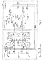
- Fig. 3 shows the one already mentioned U.S. Patent US 4,229,706 described symmetric-structure audio-balanced power amplifier, which is DC-coupled in the two signal paths and whose two npn-output stage transistors Q1, Q2 are each fed by a floating power supply V1, V2.
- the galvanic separation of the ground reference potential GND is in the floating power supply usually by means of its own power transformer and a bridge rectifier circuit reached.
- the load RL is connected between the two emitters, which also form the bases for the cross-connected floating supply voltages V1, V2.
- the balanced input signal is fed via the inputs + in and -in, the positive input + in being connected to the non-inverting input of an operational amplifier U1 implemented in bipolar technology.
- the negative input -in is connected to the non-inverting input of a second operational amplifier U2 identical to the first operational amplifier U1.
- the output of the first and second operational amplifier is connected directly, ie without a coupling capacitor, to the base of the first and second output transistors Q1, Q2.
- the voltage supply of the two operational amplifiers via two series-connected voltage sources V3, V4, the node of which is connected to the ground potential GND and the mass-remote poles form the positive and negative supply voltage + V, -V for the two operational amplifiers U1, U2.
- the quiescent current setting of the two output transistors Q1, Q2 takes place in each case via a resistor R4 or R5 between the emitter and the negative supply voltage -V.
- the associated base current supplies the output of the associated operational amplifier U1 or U2. This presents a problem now, since the current determined by the resistor R4 or R5 must be identical to the base current supplied by the operational amplifier U1 or U2, since this current is only linked to the voltage sources V3, V4 and no other current path is available stands. So it is not regulated the emitter quiescent current, but the base current.
- the resulting emitter quiescent current which is essentially supplied by the floating voltage supply V1 or V2 and flows back via the load RL, is directly dependent on the current amplification factor of the respective output transistor Q1 or Q2 and diffuses therewith, which is actually undesirable.
- the current regulation strictly speaking the regulation of the base current, is effected by tapping off the respective emitter potential and returning it via a relatively high-resistance resistor R2 or R3 to the inverting input of the first or second operational amplifier U1, U2.
- both emitters which also form the connection points for the load RL, are as close as possible to the same potential
- these two circuit nodes are also connected to one another via a relatively high-resistance resistor R6 and thus the difference of the two potentials as a kind of offset voltage to the inverting Inputs of the operational amplifier U1, U2 returned.
- the relatively small quiescent current not the modulation of the Output transistors Q1, Q2 obstructed, increases the respective emitter current through a resistor diode path R7, D1 and R8, D2, which provides the respective emitter a lower resistance current path to ground GND available when the diode becomes conductive.
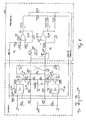
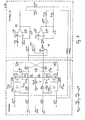
- Fig. 4 schematically shows the circuit diagram of a first embodiment of a balanced push-pull amplifier according to the invention.
- the two signal paths are constructed symmetrically and each contain a preamplifier block N1B or N2B and a power amplifier M1 or M2.
- the power amplifiers M1, M2 are each connected to a floating power supply V1, V2, wherein the load circuits via a load RL, which is connected between the bases of the two power amplifiers M1, M2, are cross-closed.
- the two base points of the power amplifiers also represent the connection points or terminals RL1, RL2 for the externally connected load RL and form the signal output.
- the voltage supply device of the preamplifier blocks N1B, N2B contains at least two series-connected voltage sources V3, V4 whose connection point is connected to ground GND.
- the resulting supply voltages + Ub and -Ub feed the supply terminals of the preamplifier blocks, which in the embodiment of Fig. 4 each consist of an input side amplifier N1, N2 with high open-loop gain.
- the positive pole of the output stage of the amplifiers N1, N2 is supplied with the positive supply voltage + Ub or with another positive and earth-related voltage source.
- the negative pole of the output stage of the amplifiers N1, N2 is connected via a potential difference generator 4, 5 to the associated load terminal RL1, RL2. About this potential difference generator 4, 5 flows an impressed current.
- the amplifiers N1, N2 Due to the high open-loop gain in conjunction with a high-impedance non-inverting and high-impedance inverting input, with negligible offset voltage and negligible offset current and with a low-impedance output, the amplifiers N1, N2 have a behavior like a more or less ideal operational amplifier.
- the first power amplifier M1 is powered by a floating first voltage source V1 and the second power amplifier M2 is powered by a floating second voltage source V2.
- the first power amplifier M1 is connected via its first supply terminal to one pole of the first voltage source V1 and via its second supply terminal, which also serves as a power amplifier output, to the first output RL1 and via the load RL to the other pole of the first voltage source V1.
- the second power amplifier M2 is connected via its first supply terminal to a pole of the second voltage source V2 and via its second supply terminal, which also serves as a power amplifier output, to the second output RL2 and via the load RL to the other pole of the second voltage source V2,
- the required operating point-determining control voltage is determined in the associated potential difference generators 4, 5 by a predetermined by a quiescent current setting Ix with an adjustable current source I1, which generates the desired potential offset via the potential difference generator 4, 5.
- the closed-circuit current setting device Ix connected to the negative supply connection -Ub contains an adjustable current source I1 whose current is split in half between the two potential difference generators 4, 5 by means of the two resistors R2, R3 connected to the output terminals RL1, RL2, so that the operating point setting for the two Power amplifier M1, M2 takes place symmetrically.
- a temperature-influenced control which, via a temperature sensor which detects the temperature of at least one power component, influences the adjustable current or voltage source I1 or Vbias such that the quiescent current of the power components of the power amplifiers M1, M2 remains constant or has a predetermined temperature profile
- a complete automatic control is such that the current quiescent current value of the power components of the power amplifiers M1, M2 is measured and compared with a predetermined setpoint and deviations occurring from the setpoint by automatically adjusting the quiescent current setting Ix away become.
- the two amplifiers N1 and N2 have an inverting and a non-inverting input and, because of their high open-loop gain, each correspond to an operational amplifier.
- the output of the resulting operational amplifier is most suitably the load connection RL1 or RL2, which is controlled by a feedback network to the ground potential GND.
- the feedback network is formed by the series-connected resistors R6 and R7 or R8 and R9, which are connected between the load terminal RL1 and ground GND and the load terminal RL2 and ground GND.
- the common connection point of the resistors R6, R7 and R8, R9 is connected to the inverting input of the amplifier N1 and N2, respectively.
- the non-inverting input of the first amplifier N1 is connected to the positive signal input + in and the non-inverting input of the second amplifier N2 is connected to the negative signal input -in of the push-pull amplifier.
- the feedback network R6, R7 and R8, R9 the output of the amplifier N1 or N2 is controlled so that the potential at the noninverting input of the amplifier N1 or N2 via the potential difference generator 4, 5 and the voltage divider R6, R7 and R8, R9 N2 is identical to the potential at the positive or negative signal input + in or -in.
- This regulation via the feedback network is independent of the magnitude of the quiescent current setting for the power components of the power amplifiers M1, M2, which is predetermined by the adjustable current source I1.
- the resulting level offset at the potential difference generator 4 or 5 is regulated by the amplifier N1 or N2.
- the resistors R10 and R11 from the positive and negative signal input to ground GND have no meaning for the feedback. They merely serve to determine the GND potential for the respective non-inverting inputs of N1 and N2 and the line adaptation, since the signal inputs at the non-inverting inputs of the amplifiers N1 and N2 are usually high-impedance.
- An embodiment is shown below in which the signal inputs are connected to the inverting inputs of the amplifiers N1 and N2. By connected to these inputs feedback network these inputs are then much lower impedance, so that a line adjustment may be omitted if necessary.
- the ratio of the resistors R6 / R7 and R8 / R9 determines the overall gain of the push-pull amplifier.
- the upper amplifier half consisting essentially of the modules N1B and M1, amplifies the one half-wave of the balanced input signal and the lower amplifier half, consisting of the modules N2B and M2, amplifies the other half-wave.
- the power amplifiers M1, M2 can be practically implemented in a variety of ways: as individual power devices such as power electronics. Power MOSFETs, IGBTs or bipolar power transistors, but also advantageous combinations of similar or different amplifier components with or without local negative feedback.
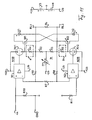
- the output stages of the preamplifier blocks N1B and N2B are exemplified as triode Xtr1 and Xtr2, respectively.
- the preamplifier blocks N1B and N2B thus each consist of the combination of an input-side amplifier N1, N2 with high open-loop gain and a connected to the amplifier N1, N2 tube Xtr1, Xtr2, the control grid is connected to the associated amplifier output.
- the anode of the tube Xtr1, Xtr2 is connected to the positive supply voltage + Ub or to another positive and also earth-related voltage source.
- the cathode of the tube Xtr1, Xtr2 is connected to the associated load terminal RL1, RL2 via a potential difference generator 4, 5 which in the simplest case contains a resistor R4, R5 and through which an impressed current flows.
- tetrodes pentodes, hexodes and heptodes can also be used as circuits of the additional gratings corresponding to the prior art as tubes Xtr1, Xtr2 shown as triodes.
- FIG. 5 show two n-channel MOSFETs whose respective gate electrode is connected to the cathode of the preceding tube Xtr1, Xtr2.
- the respective source electrode is connected to the associated load terminal RL1, RL2 and the respective drain electrode to the positive potential of floating voltage source V1, V2 connected.
- the operating point-determining gate-source control voltage is determined in the associated potential difference generators 4, 5 by a predetermined by a quiescent current setting Ix with an adjustable current source I1, which generates the desired potential offset via the resistors R4, R5.
- the quiescent current adjuster Ix connected to the negative supply terminal -Ub contains an adjustable current source I1 whose current is split in half by means of the two resistors R2, R3 connected to the output terminals RL1, RL2 to the two resistors R4, R5, so that the operating point setting for the two MOSFETs M1, M2 takes place symmetrically.
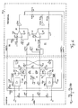
- the circuit block B1 includes two control circuits B2, B3 whose inputs are coupled to the amplifier outputs RL1, RL2 and their outputs to the feedback networks of the two preamplifier blocks N1B and N2B, respectively.
- the input of the first control circuit B2 is formed by two series-connected equal resistors R16, R17, which are connected to the outputs RL1, RL2 and the common connection point avg is connected via a resistor R15 to the inverting input of an operational amplifier U3.
- a DC voltage V5 is applied at the non-inverting input of U3 .
- the output of the amplifier U3 is fed back to the non-inverting input by means of a capacitor C2.
- the voltage supply of the amplifier U3 is expediently carried out via the already existing supply potentials + Ub and -Ub or via another supply voltage.
- the input of the second control loop B3 is formed by a subtractor D1, whose minimum input + to the load terminal RL2 and whose subtrahende input - to the load terminal RL1 is connected.
- the output of the subtracter D1 determines the potential of the node diff and is connected via a resistor R14 to the inverting input of an amplifier U4, which is connected via a capacitor C1 to its amplifier output.
- This output is further connected via a series circuit of an inverter N4 and a resistor R12 to the circuit node bias 1 and via a resistor R13 to the other circuit node bias 2.
- the ground potential GND is connected.
- the inventive function of the control block Biasregelung B1 is that by means of the first control loop B2 of the average avg of the potentials detected at the outputs RL1, RL2 and compared with a predetermined target voltage V5.
- the deviation of the potential avg from the desired value V5 is amplified via the integrator formed by the amplifier U3.
- this amplified deviation from the desired value V5 acts in the same way on the two directly coupled control interfaces bias 1 and bias 2, that the mean value of the potentials at the output terminals RL1, RL2 to the predetermined target value V5 is adjusted.
- the absolute value of the absolute value of the outputs RL1, RL2 is set defined.
- ⁇ 2 greater than or equal to 1s makes sense.
- the amplifiers N1 or N2 are implemented in the preamplifier blocks in such a way that a considerable drift-loaded potential difference between the non-inverting and inverting inputs of these amplifiers N1, N2 occurs at rest, this can have a disturbing influence on the Working point stability can be minimized.
- the first stage of a tube amplifier could be realized as a cathode base stage.
- the grid corresponds to the non-inverting input of the amplifier N1 or N2 and the cathode corresponds to the inverting input of N1 or N2.
- the cathode current results in a potential increase across the resistor R7 or R9.
- the operating points of tubes are subject to thermal and aging-related fluctuations.
- the current component I (R6) or I (R8) changes via the temperature and the aging of the input tubes, which essentially bring about the voltage amplification in the amplifiers N1 or N2, and thus according to the first relationship, that indicated by I (R4 ) certain potential of the gate-source path of the power amplifier M1.
- the potential determined by the current I (R5) has an effect on the gate-source path of the final amplifier M2.
- the setpoint voltage V5 is not fixed, but as in the exemplary embodiment of FIG Fig.
- control interfaces bias 1 and bias 2 are interconnected via the series-connected equal resistors R24 and R25, so that a new node voltage avgln for a third control loop B4 is available at the common resistor tap.
- This node voltage avgln is fed via a resistor R26 to the non-inverting input of the control amplifier U3, which is different than in Fig. 5 is not supplied with a reference voltage V5, but generates its reference voltage at this terminal itself by a capacitor C3 is connected there.
- the mean value of the potentials at the control interfaces bias 1 and bias 2 is thus low-pass filtered via the RC element R26 and C3 and then serves as a reference voltage at the noninverting input of the control amplifier U3.
- the corner frequency of the RC element R26, C3 is preferably chosen lower than the lowermost to be transmitted useful signal frequency at least a decade.
- the fundamental or drift-related potential difference between the inputs of the amplifiers N1 and N2, to which a portion of the output voltage is fed back via the negative feedback network, and the output nodes RL1 and RL2, respectively, are ideally regulated to zero or at least so small that the error component is thereby reduced the quiescent current control has no influence.
- Fig. 7 an embodiment of the push-pull amplifier is shown, which has as output amplifiers M1, M2 respectively tubes Xtr3, Xtr4, which directly drive the load RL.
- the preamplifier blocks N1B, N2B contain, in contrast to the preceding embodiments Fig. 5 and Fig. 6 no combination amplifier, but consist solely of the amplifiers N1, N2. These are realized so that they have a negative DC output voltage of several volts to several tens of volts depending on the connected tubes Xtr3, Xtr4 at rest.
- the adjustable current source I1 is connected to a positive potential + Ub, so that half its current flows via the resistors R2, R3, the level converters 4, 5 and the internal output stage from N1, N2 to the negative supply voltage -Ub.
- This current flow causes the required negative grid bias on the resistors R4, R5 for the tubes Xtr3 and Xtr4, respectively. It is thus again defined with only one manipulated variable of the quiescent current of both tubes Xtr3, Xtr4 in the floating without fixed ground reference driven amplifiers M1, M2 and set synchronously and symmetrically.
- the quiescent current of the tubes Xtr3, Xtr4 can be performed in a variety of ways manually, temperature-controlled or by means of an automatic quiescent current control loop.
- triodes were used.
- Xtr3, Xtr4 but all known tube types such as tetrodes and pentodes can be used.
- the load RL has to be coupled by means of a transformer to the tube-equipped power output stage M1, M2 in a special requirement, this can be done with the same structure as in FIG Fig. 7 take place, except that instead of the direct load coupling a transformer down-converted in a known manner, the internal resistance of the tube output stage to the low-impedance load.
- the transformer can be performed cost saving as autotransformer, since no Gleichstromvormagnetmaschine occurs by the quiescent current adjustment according to the invention.
- the autotransformer is wound symmetrically, for example in a two-chamber design, so that the same winding resistances result for both winding halves. Due to the lack of DC biasing, a realization as a toroidal transformer is also possible.
- the winding is in this case divided into integer equal parts, which are then wound in pairs bifilar.
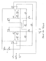
- FIG. 8 Another embodiment of the push-pull amplifier according to the invention shows Fig. 8 , This circuit is almost identical to the circuit of Fig. 6 , except that the manipulated variable for the quiescent current setting is not as in Fig. 6 is carried out by the adjustable current source I1, but by an adjustable voltage source Vbias, but ultimately via the resistors R2, R3 also generates a current that is split in half by means of these resistors R2, R3 and the resistors R4, R5 the desired operating point determining potential offset for generates the respective gate-source path of the two n-channel MOSFETs in the power amplifier M1, M2.
- the absolute value of the potentials at the load terminals RL1, RL2 is defined and adjusted to an approximately equal value. Since the resistors R2 and R3 are equal to each other, the currents I (R2) and I (R3) flowing therethrough are also equal to each other. These currents flow almost completely through the resistors R4 and R5 and from the cathode to the anode of the triode Xtr1 and Xtr2 to the positive operating voltage + Ub. Due to the resulting potential offset at the resistors R4 and R5, a defined positive potential difference between the gate-source path of the MOSFETs M1 and M2 is generated, and consequently a defined quiescent current flows through these output stage transistors. The adjustment process of the voltage source Vbias can again take place in a variety of ways, manually, temperature-controlled or by means of an automatic quiescent current control loop.
- a push-pull amplifier according to the invention can also be realized in that the input-side amplifiers N1, N2 in the preamplifier blocks N1B, N2B are each connected with their inverting amplifier input to the signal inputs -in or + in the push-pull amplifier.
- the input area of the amplifiers N1, N2 only minor circuit changes have to be made.
- the resistors R7 and R9 of the feedback networks are now not connected to the ground potential as for example, in the comparable Fig. 5 but to the negative or positive signal input -in or + in the push-pull amplifier.
- the resistors R10 and R11 at the non-inverting inputs of the amplifiers N1 and N2 are connected at the ends remote from the amplifier to the ground potential GND. Furthermore, the recirculated lines of the rule interfaces bias 1 and bias 2 are no longer as in Figure 5 to the inverting input of the amplifier N1 or N2, but to their non-inverting inputs.
- the control currents fed back by the control circuits B2 and B3 generate the required control voltages for the amplifiers N1, N2 via the resistors R10 and R11, respectively.
- Fig. 10 shows a further variant of the quiescent current setting.
- the basic circuit of this push-pull amplifier is approximately comparable to the circuit of Fig. 5 ,
- the potential difference generators 4 and 5 each contain an optoelectronic component OK1 or OK2 or are coupled to such components.
- the light emission is controlled in each case an LED element, is dependent on the intensity of the volume resistivity of a photosensitive photo-transistor.
- This photo-transistor is parallel to that of already Fig. 5 known resistor R4 or R5, which is fed via the likewise known resistor R2 or R3, but its base point in contrast to Fig. 5 on the negative fixed potential -Ub.
- the potential difference generator 4 and 5 are thus formed by an assembly that combines the resistors R4 and R5 each with an opto-coupler distance OK1 and OK2 in itself.
- a synchronous adjustment of the quiescent current of both branches of the floating voltage-supplied power amplifier is carried out by the application of both optocouplers with the same control or regulating current.
- the current equality is in the exemplary embodiment after Fig. 10 thereby forced that the current of the adjustable current source I1 from the negative supply terminal -Ub is looped through both optocouplers OK1, OK2 to the positive supply terminal + Ub.
- the embodiment according to Fig. 11 shows an advantageous arrangement of the push-pull amplifier according to the invention, when in principle only unbalanced input signals to be processed instead of symmetrical input signals.
- the circuit is suitable for Fig. 5 , In order for both signal branches to be able to operate simultaneously, ie at each half-wave, the amplifier N1 at the non-inverting input and the amplifier N2 at the inverting input are driven.
- the non-inverting input of the amplifier N1 is connected to the signal input + in and via the resistor R10 to the ground potential GND.
- the inverting input of the amplifier N1 is as in Fig.
Abstract
Description
Die wesentlichen Qualitätskriterien für Leistungsverstärker, insbesondere bei Anwendungen im Audiobereich, sind ein möglichst geringer Klirrfaktor, eine hohe Bandbreite, ein möglichst geringer Innenwiderstand, möglichst geringe transiente Intermodulationsverzerrungen und eine hohe Arbeitspunktstabilität der Leistungsbauelemente.The essential quality criteria for power amplifiers, in particular for applications in the audio sector, are the lowest possible total harmonic distortion, a high bandwidth, the lowest possible internal resistance, the lowest possible transient intermodulation distortion and a high operating point stability of the power components.
Leistungsverstärker können mit sehr unterschiedlichen aktiven Bauelementen aufgebaut werden, deren Eigenschaften in der Regel die Struktur des Verstärkers bestimmen: Röhren mit unterschiedlichem Aufbau, z.B. Trioden, Tetroden, Pentoden, oder Halbleiterbauelemente, z.B. Bipolartransistoren, Feldeffekttransistoren, MOSFETs und IGBTs. Röhren haben für den Einsatz als Leistungsverstärker in der Regel einen vergleichsweise hohen Innenwiderstand und müssen deshalb mit Hilfe von speziell aufgebauten Transformatoren, den Übertragern, an die niedrige Impedanz des Lautsprechers angepasst werden. Diese Übertrager begrenzen indessen die erzielbare Bandbreite und sind selbst Quelle erheblicher nichtlinearer Verzerrungen. Die deshalb wünschenswerte direkte Ankopplung der in der Regel niederohmigen Last des Lautsprechers erfordert die Verwendung von aktiven Bauelementen mit möglichst geringem Innenwiderstand bzw. möglichst großer Steilheit. Aus diesem Grund hat sich als Stand der Technik die Verwendung von Halbleiterbauelementen wie Bipolartransistoren, MOSFETs oder in selteneren Fällen auch IGBTs durchgesetzt.Power amplifiers can be constructed with very different active devices, the characteristics of which usually determine the structure of the amplifier: tubes of different construction, e.g. Triodes, tetrodes, pentodes, or semiconductor devices, e.g. Bipolar transistors, field effect transistors, MOSFETs and IGBTs. Tubes usually have a comparatively high internal resistance for use as power amplifiers and therefore have to be adapted to the low impedance of the loudspeaker with the aid of specially constructed transformers, the transformers. However, these transmitters limit the achievable bandwidth and are themselves the source of significant nonlinear distortions. The therefore desirable direct coupling of the usually low-impedance load of the loudspeaker requires the use of active components with the lowest possible internal resistance or the greatest possible steepness. For this reason, the use of semiconductor components such as bipolar transistors, MOSFETs or, more rarely, IGBTs has prevailed as state of the art.
Besonders häufig werden Verstärker mit höheren Leistungsanforderungen als komplementäre Gegentaktverstärker realisiert, wobei komplementäre Bipolartransistoren (npn- und pnp-Transistor) oder komplementäre MOSFETs (n-Kanal- und p-Kanal-Transistor) oder komplementäre IGBTs (n-Kanal- und p-Kanal-Typ) mit einer auf Massepotential bezogenen bipolaren oder unipolaren Betriebsspannungsquelle eingesetzt werden.More frequently, amplifiers with higher power requirements than complementary push-pull amplifiers are realized, with complementary bipolar transistors (npn and pnp transistor) or complementary MOSFETs (n-channel and p-channel transistor) or complementary IGBTs (n-channel and p-channel Type) with a bipolar or unipolar operating voltage source related to ground potential.
Das gemeinsame Merkmal des in
In der Grundschaltung von
In der Grundschaltung von
Am zuletzt genannten Merkmal ändert sich auch nichts wesentliches durch das Einfügen eines sehr niederohmigen Messwiderstandes zwischen dem Lastwiderstand bzw. dem Lautsprecher und der Masse, wie dies in einigen Publikationen zur Strommessung vorgeschlagen wird.At the last mentioned feature, nothing essential changes by the insertion of a very low-impedance measuring resistor between the load resistor and the speaker and the ground, as proposed in some publications for current measurement.
Komplementäre Gegentaktendstufen mit Röhren gibt es nicht, da Röhren entsprechend dem Elektronenfluss zwischen Kathode und Anode nur einen negativen Strom steuern, so dass ein zur Elektronenröhre komplementäres Verstärkerelement fehlt.There are no complementary push-pull power amplifiers with tubes since tubes only control a negative current according to the electron flow between the cathode and the anode, so that an amplifier element that is complementary to the electron tube is missing.
Für die Realisierung hochlinearer Leistungsverstärker wäre der Einsatz von Röhren als Spannungsverstärker jedoch sehr wünschenswert, da in diesem Anwendungsfall Röhren wegen ihrer quadratischen Strom-Spannungskennline sehr verzerrungsarm betrieben werden können. Optimal wäre die Kombination von Röhren als Spannungsverstärker mit hochsteilen Halbleiterbauelementen, wie Bipolartransistoren, MOSFETs oder IGBTs, als ausgangsseitiger Leistungsverstärker. Von großem Vorteil wäre hierbei eine Gleichstromkopplung zwischen den einzelnen Verstärkungsstufen, damit die ansonsten für die Potentialtrennung erforderlichen Kopplungs- oder Überbrückungskondensatoren oder Übertrager keinen schädlichen Einfluss auf den Frequenzgang oder den Klirrfaktor haben.
Die bisherigen Entwicklungen konzentrierten sich auf die Optimierung von reinen Transistorverstärkern einerseits und reinen Röhrenverstärkern andererseits. Daneben sind auch vereinzelt Verstärker mit hybrider Bauelementebestückung bekannt, die getrennt nach Röhren- bzw. Transistorverwendung optimierte Vor- und Leistungsverstärker enthalten, die in der Regel kapazitiv miteinander gekoppelt sind.For the realization of highly linear power amplifiers, however, the use of tubes as a voltage amplifier would be very desirable, since in this application, tubes can be operated very low distortion because of their square current-voltage characteristic. Optimal would be the combination of tubes as a voltage amplifier with hochsteil semiconductor devices, such as bipolar transistors, MOSFETs or IGBTs, as output side power amplifier. Of great advantage here would be a DC coupling between the individual gain stages, so that otherwise required for the potential separation coupling or bypass capacitors or transformers have no harmful effect on the frequency response or harmonic distortion.
The developments so far concentrated on the optimization of pure transistor amplifiers on the one hand and pure tube amplifiers on the other hand. In addition, occasionally amplifiers with hybrid component assembly are known, which contain separately after tube or transistor use optimized pre and power amplifiers, which are usually capacitively coupled together.
Bei den komplementären Gegentaktendstufen gemäß
Ein Problem bei der Suche nach einem möglichst symmetrischen komplementären Transistorpaar ist die sehr begrenzte Auswahl an pnp-Bipolartransistoren, p-Kanal-MOSFETs und p-Kanal-IGBTs für hochwertige Leistungsverstärker. Dieses Problem wird durch den Aufbau einer quasikomplementären Leistungsstufe nicht behoben, sondern auf Kosten der Symmetrie nur in die Treiberstufe verlagert. Die in der Realität verwendbaren Paare komplementärer Transistoren sind bei näherer Analyse keineswegs echte Paare. So unterscheiden sich die komplementären Transistoren eines Komplementärpaares zum Beispiel maßgeblich hinsichtlich des Betrages des Stromverstärkungsfaktors bei Bipolartransistoren bzw. der Steilheit bei MOSFETs und IGBTs. Dies ist eine wesentliche Ursache für Nichtlinearitäten im Verstärkerverhalten.A problem in the search for the most symmetrical pair of complementary transistors is the very limited choice of pnp bipolar transistors, p-channel MOSFETs and p-channel IGBTs for high quality power amplifiers. This problem is not resolved by the construction of a quasi-complementary power level, but shifted at the expense of symmetry only in the driver stage. The pairs of complementary transistors which can be used in reality are by no means real pairs on closer analysis. For example, the complementary transistors of a complementary pair differ substantially in terms of the magnitude of the current amplification factor in the case of bipolar transistors and the transconductance in MOSFETs and IGBTs. This is a major cause of nonlinearities in amplifier performance.
Beispielsweise ist bei gleicher Drain-Source-Spannungsfestigkeit, gleichem zulässigen maximalen Drainstrom sowie gleicher maximal zulässiger Verlustleistung die Chipgröße von p-Kanal-MOSFETs ca. dreimal größer als die Chipfläche des komplementären n-Kanal-MOSFETs. Das führt zwangsläufig zu erheblich unterschiedlichen Kapazitäten, insbesondere der Gate-Source-Kapazität und der Drain-Source-Kapazität. Durch die unterschiedlichen kapazitiven Lasten resultieren Probleme bei der Ansteuerung und ohne weitere Schaltungsmaßnahmen ergeben sich unterschiedliche Flankensteilheiten (= Slew-Rate) für positive und negative Flanken am Verstärkerausgang. Wird ein solcher Verstärker gegengekoppelt, wird die Frequenzkompensation von den erheblich größeren Kapazitäten des negativen Zweiges (p-Kanal MOSFETs bzw. -IGBTs) bestimmt. Das kann die erreichbare Leistungsbandbreite unzulässig stark reduzieren oder zu Instabilitäten führen. Bei Bipolartransistoren sind diese Anpassprobleme (=Matching-Probleme), die für die komplementäre Symmetrie erforderlich sind, ähnlich.For example, with the same drain-source dielectric strength, the same permissible maximum drain current and the same maximum allowable power loss, the chip size of p-channel MOSFETs is approximately three times greater than the chip area of the complementary n-channel MOSFET. This inevitably leads to significantly different capacities, in particular the gate-source capacitance and the drain-source capacitance. By the Different capacitive loads result in problems in the control and without further circuit measures, different slew rates result (= slew rate) for positive and negative edges at the amplifier output. If such an amplifier is fed back, the frequency compensation is determined by the considerably larger capacities of the negative branch (p-channel MOSFETs or -IGBTs). This can unduly reduce the achievable power bandwidth or lead to instabilities. For bipolar transistors, these matching problems (= matching problems), which are required for complementary symmetry, are similar.
Zusammenfassend ist festzustellen, dass die dem Stand der Technik entsprechenden Gegentaktverstärker in Komplementärtechnik prinzipbedingt keine vollständige Symmetrie erreichen können. Es sind einige Verfahren bekannt, welche die daraus resultierenden Nichtlinearitäten mittels einer Gegenkopplung und/oder einer Vorwärtsfehlerkompensation (= Forward-Error-Correction) zu beheben versuchen. Der dafür notwendige Schaltungsaufwand ist für hochqualitative Leistungsverstärker allerdings sehr hoch. Desweiteren ist die korrekte Arbeitsweise der Fehlerkompensation bei der für Audio-Anwendungen typischen Ansteuerung mit transienten Impulsen kritisch. So ist beispielsweise in der
Übertragerlose Gegentaktleistungsverstärker, die aktive Bauteile nur eines Leitfähigkeitstyps verwenden und die damit streng symmetrisch bezüglich der elektrischen Eigenschaften realisierbar sind, wurden bislang insbesondere mit Röhren auf den Markt gebracht. Sie werden allgemein als OTL-Verstärker bezeichnet (= Output Transformer-Less) und unter dieser Bezeichnung kommerziell angeboten. Röhrenverstärker, die nach diesem Prinzip gebaut sind, weisen folgende grundsätzlichen Nachteile auf: Röhren haben eine zu geringe Steilheit, um die niederohmige Impedanz des Lastwiderstandes bzw. des Lautsprecher direkt anzusteuern. Ohne weitere Schaltungsmaßnahmen resultieren hieraus eine geringe abgebbare Leistung und ein sehr hoher Klirrfaktor.Transformerless push-pull power amplifiers, which use active components of only one conductivity type and which can thus be realized strictly symmetrical with respect to the electrical properties, have hitherto been marketed, in particular with tubes. They are commonly referred to as OTL amplifiers (= Output Transformer-Less) and commercially available under this name. Tube amplifiers built according to this principle have the following basic disadvantages: Tubes have too low a slope to directly control the low impedance of the load resistor or loudspeaker. Without further circuitry, this results in a low deliverable power and a very high harmonic distortion.
Um die Steilheit zu erhöhen, werden viele Röhrensysteme parallel geschaltet. Damit lässt sich bei exzessiv parallel geschalteten Röhren bzw. Röhrensystemen die Steilheit des daraus resultierenden Leistungsbauelementes auf einen gerade ausreichenden Wert erhöhen. Der Klirrfaktor bleibt aber immer noch hoch. Es gibt nun aber erhebliche Probleme mit der Stabilität der Arbeitspunkte der vielen Röhrensysteme. Die thermische Drift des Anodenstromes bei vorgegebener Gittervorspannung und die Änderung der Röhreneigenschaften infolge von Alterung, wie z.b. nachlassende Katodenemissionsfähigkeit, führen im günstigsten Fall zu einem erhöhten Klirrfaktor, im ungünstigsten Fall zum Totalausfall des Gerätes.To increase the steepness, many tube systems are connected in parallel. In the case of excessively parallel tubes or tube systems, the steepness of the resulting power component can thus be increased to a just sufficient value. The harmonic distortion is still high. However, there are considerable problems with the stability of the operating points of the many tube systems. The thermal drift of the anode current at a given grid bias and the change in tube properties due to aging, such as. decreasing cathode emissivity lead in the best case to an increased harmonic distortion, in the worst case total failure of the device.
Der Arbeitspunkt der Leistungsstufe wird bei diesen Röhrenschaltungen mittels einer festen Gittervorspannung wie beispielsweise im
Die nach dem Stand der Technik in Röhrenschaltungen unausweichliche Verwendung von Koppel- und/oder Überbrückungskondensatoren verschlechtern die erreichbare Linearität erheblich. Wie
Im
Die in
Die Art der realisierten Ruhestromeinstellung funktioniert ausschließlich mit Bipolartransistoren, da die Höhe des Basisstromes (Stromfluss der Basis-Emitterstrecke) über den Treiber und das Widerstandsnetzwerks gesteuert wird.The type of quiescent current setting implemented works exclusively with bipolar transistors, since the level of the base current (current flow of the base-emitter path) is controlled via the driver and the resistor network.
Die ausschließliche Ruhestromeinstellung über die Steuerung des Basisstromes funktioniert in kreuzgekoppelten Verstärkern nur unter Verwendung ideal gleicher bipolarer Leistungstransistoren. In der Realität wird die unvermeidliche Streuung des Stromverstärkungsfaktors absolut und in Abhängigkeit von der Temperatur zu erheblichen Abweichungen zwischen den Ruheströmen der beiden Leistungstransistoren führen. Damit entsteht ein nicht vertretbar hoher Differenzfehlstrom durch den Lastwiderstand des angeschlossenen Lautsprechers.The exclusive bias current setting via the base current control works in cross coupled amplifiers only using ideally identical bipolar power transistors. In reality, the inevitable dispersion of the current gain factor will result in absolute and temperature dependent deviations between the quiescent currents of the two power transistors. This creates an unacceptably high differential leakage current through the load resistance of the connected loudspeaker.
Darüber hinaus ist die ausschließliche Verwendung von Halbleiterbauelementen in der Schaltung nach dem
In
Der Arbeitspunkt der MOSFETs wird mittels einer fixen Gatespannung über einen Spannungsteiler einerseits (vgl.
Die in
Aufgabe der Erfindung ist die Angabe eines verbesserten Gegentaktverstärkers, der einen vollsymmetrischen Aufbau mit Funktionseinheiten gleichen Leitungstyps aufweist, möglichst große Freiheit für den Einsatz von Röhren und/oder Halbleitern und/oder monolithisch integrierten Schaltungen zulässt, einen transformatorlosen Anschluss der Last ermöglicht und auf Kopplungs- sowie Überbrückungskondensatoren und Übertrager verzichtet.The object of the invention is to provide an improved push-pull amplifier, which has a fully symmetrical design with functional units of the same conductivity type, allows the greatest possible freedom for the use of tubes and / or semiconductors and / or monolithic integrated circuits, allows a transformerless connection of the load and coupling to coupling and bypass capacitors and transformers omitted.
Die Lösung der Aufgabe erfolgt nach den Merkmalen des Anspruchs 1. Die Vorteile der Erfindung bestehen darin, dass durch die vorgeschlagenen Verbesserungen ein Leistungsverstärker mit sehr hoher Linearität, der vorzugsweise als Audioverstärker der höchsten Qualitätskategorie dient, realisiert wird. Die Arbeitspunkte sind auf einfache Weise einstellbar, wobei restliche Unsymmetrien der Funktionseinheiten über zusätzliche Regeleinrichtungen sicher stabilisierbar sind. Die Regeleinrichtungen können auch so ausgebildet werden, dass sie Änderungen durch Drift und Temperatur ausgleichen können. Durch die geforderte Flexibilität lassen sich für die Vorverstärkerblöcke und die Endverstärker jeweils die zweckmäßigsten Bauelemente verwenden und miteinander kombinieren. Ob der Leistungsverstärker grundsätzlich mit einem symmetrischen Differenzsignal um den Massebezugspegel angesteuert wird oder ob dem Differenzsignal ein Gleichpegel überlagert ist oder ob ein unipolares Ansteuersignal vorliegt, erfordert allenfalls geringfügige Änderungen in den beiden Signalpfaden oder in den Regeleinrichtungen.The object is achieved by the features of
Die Erfindung und vorteilhafte Ausgestaltungen und Weiterbildungen werden nun anhand der Figuren der Zeichnung näher erläutert:
-
Fig. 1 und Fig. 2 zeigen schematisch zwei bekannte Komplementärverstärker, -
Fig. 3 zeigt schematisch einen bekannten Gegentaktverstärker mit identischen und DC-gekoppelten Funktionseinheiten und mit Kreuzkopplung in der Leistungsstufe, -
Fig. 4 zeigt schematisch ein erstes Ausführungsbeispiel der Erfindung, -
Fig. 5 zeigt schematisch ein Ausführungsbeispiel mit einer Offsetspannungsregelung, -
Fig. 6 zeigt ein Ausführungsbeispiel mit einer erweiterten Offsetspannungsregelung, -
Fig. 7 zeigt ein Ausführungsbeispiel mit Röhren in der Leistungsstufe, -
Fig. 8 zeigt ein Ausführungsbeispiel mit einer geänderten Ruhestromeinstellung, -
Fig. 9 zeigt ein Ausführungsbeispiel mit geänderten Eingangsanschlüssen, -
Fig. 10 zeigt ein Ausführungsbeispiel mit Optokopplern zur Ruhestromeinstellung und -
Fig. 11 zeigt ein Ausführungsbeispiel mit einem unsymmetrischen Signaleingang.
-
Fig. 1 and Fig. 2 schematically show two known complementary amplifiers, -
Fig. 3 shows schematically a known push-pull amplifier with identical and DC-coupled functional units and with cross-coupling in the power stage, -
Fig. 4 schematically shows a first embodiment of the invention, -
Fig. 5 shows schematically an embodiment with an offset voltage control, -
Fig. 6 shows an embodiment with an extended offset voltage control, -
Fig. 7 shows an embodiment with tubes in the power stage, -
Fig. 8 shows an embodiment with a modified closed-circuit current setting, -
Fig. 9 shows an embodiment with modified input terminals, -
Fig. 10 shows an embodiment with optocouplers for quiescent current setting and -
Fig. 11 shows an embodiment with an unbalanced signal input.
Der bekannte Komplementärverstärker von
Der bekannte Komplementärverstärker nach
Die Ruhestromeinstellung der beiden Ausgangstransistoren Q1, Q2 erfolgt über jeweils einen Widerstand R4 bzw. R5 zwischen dem Emitter und der negativen Versorgungsspannung -V. Den zugehörigen Basisstrom liefert der Ausgang des zugehörigen Operationsverstärkers U1 bzw. U2. Hier zeigt sich nun ein Problem, denn der durch den Widerstand R4 bzw. R5 bestimmte Strom muss identisch mit dem vom Operationsverstärker U1 bzw. U2 gelieferten Basisstrom sein, da dieser Strom nur mit den Spannungsquellen V3, V4 verknüpft ist und kein anderen Strompfad zur Verfügung steht. Es wird also nicht der Emitterruhestrom geregelt, sondern der Basisstrom. Der resultierende Emitterruhestrom, der im wesentlichen von der schwebenden Spannungsversorgung V1 bzw. V2 gespeist wird und über die Last RL zurückfließt, ist direkt vom Stromverstärkungsfaktor des jeweiligen Ausgangstransistors Q1 bzw. Q2 abhängig und streut damit, was eigentlich unerwünscht ist. Die Stromregelung, genau genommen die Regelung des Basisstromes, erfolgt durch Abgriff des jeweiligen Emitterpotentials und Rückführung über einen relativ hochohmigen Widerstand R2 bzw. R3 auf den invertierenden Eingang des ersten bzw. zweiten Operationsverstärkers U1, U2. Damit beide Emitter, die ja auch die Anschlusspunkte für die Last RL bilden, möglichst auf gleichem Potential liegen, sind diese beiden Schaltungsknoten ebenfalls über einen relativ hochohmigen Widerstand R6 miteinander verbunden und somit wird auch die Differenz der beiden Potentiale als eine Art Offsetspannung auf die invertierenden Eingänge der Operationsverstärker U1, U2 zurückgeführt. Damit im Ansteuerungsfall der relativ kleine Ruhestrom nicht die Aussteuerung der Ausgangstransistoren Q1, Q2 behindert, vergrößert sich der jeweilige Emitterstrom durch eine Widerstands-Diodenstrecke R7, D1 bzw. R8, D2, die dem jeweiligen Emitter einen niederohmigeren Strompfad nach Masse GND zur Verfügung stellt, wenn die Diode leitend wird. Es wird noch erwähnt, das durch die in
Die Spannungsversorgungseinrichtung der Vorverstärkerblöcke N1B, N2B enthält mindestens zwei in Serie geschaltete Spannungsquellen V3, V4, deren Verbindungspunkt an Masse GND liegt. Die resultierenden Versorgungsspannungen +Ub und -Ub speisen die Versorgungsanschlüsse der Vorverstärkerblöcke, die im Ausführungsbeispiel von
Als Endverstärker M1, M2 sind in
Die erforderliche arbeitspunktbestimmende Steuerspannung wird in den zugehörigen Potentialdifferenzerzeugern 4, 5 durch einen von einer Ruhestromeinstelleinrichtung Ix mit einer einstellbaren Stromquelle I1 vorgegebenen Strom bestimmt, der über die Potentialdifferenzerzeuger 4, 5 den gewünschten Potentialversatz erzeugt. Die mit dem negativen Versorgungsanschluss -Ub verbundene Ruhestromeinstelleinrichtung Ix enthält eine einstellbare Stromquelle I1, deren Strom mittels der beiden mit den Ausgangsanschlüssen RL1, RL2 verbundenen Widerstände R2, R3 hälftig auf die beiden Potentialdifferenzerzeuger 4, 5 aufgeteilt wird, so dass die Arbeitspunkteinstellung für die beiden Endverstärker M1, M2 symmetrisch erfolgt.The required operating point-determining control voltage is determined in the associated
Dieser Einstellvorgang kann selbstverständlich auf verschiedene Weisen erfolgen, beispielsweise rein manuell wie im Ausführungsbeispiel von
Die beiden Verstärker N1 und N2 haben einen invertierenden und einen nichtinvertierenden Eingang und entsprechen wegen ihrer hohen Leerlaufverstärkung jeweils einem Operationsverstärker. Als Ausgang des resultierenden Operationsverstärkers sieht man dabei am zweckmäßigsten den Lastanschluss RL1 bzw. RL2 an, der durch ein Rückkopplungsnetzwerk auf das Massepotential GND geregelt wird. Das Rückkopplungsnetzwerk wird durch die seriengeschaltete Widerstände R6 und R7 bzw. R8 und R9 gebildet, die zwischen dem Lastanschluss RL1 und Masse GND bzw. dem Lastanschluss RL2 und Masse GND liegen. Der gemeinsame Verbindungspunkt der Widerstände R6, R7 bzw. R8, R9 ist mit dem invertierenden Eingang des Verstärkers N1 bzw. N2 verbunden. Der nichtinvertierende Eingang des ersten Verstärkers N1 ist mit dem positiven Signaleingang +in und der nichtinvertierende Eingang des zweiten Verstärkers N2 ist mit dem negativen Signaleingang -in des Gegentaktverstärkers verbunden. Durch das Rückkopplungsnetzwerk R6, R7 bzw. R8, R9 wird der Ausgang des Verstärkers N1 bzw. N2 so geregelt, dass über den Potentialdifferenzerzeuger 4, 5 und den Spannungsteiler R6, R7 bzw. R8, R9 das Potential am nichtinvertierenden Eingang des Verstärkers N1 bzw. N2 identisch zum Potential am positiven bzw. negativen Signaleingang +in bzw. -in ist. Diese Regelung über das Rückkopplungsnetzwerk ist unabhängig von der Größe der Ruhestromeinstellung für die Leistungsbauelemente der Endverstärker M1, M2, die durch die einstellbare Stromquelle I1 vorgegeben ist. Der resultierende Pegelversatz am Potentialdifferenzerzeuger 4 bzw. 5 wird durch den Verstärker N1 bzw. N2 ausgeregelt.The two amplifiers N1 and N2 have an inverting and a non-inverting input and, because of their high open-loop gain, each correspond to an operational amplifier. The output of the resulting operational amplifier is most suitably the load connection RL1 or RL2, which is controlled by a feedback network to the ground potential GND. The feedback network is formed by the series-connected resistors R6 and R7 or R8 and R9, which are connected between the load terminal RL1 and ground GND and the load terminal RL2 and ground GND. The common connection point of the resistors R6, R7 and R8, R9 is connected to the inverting input of the amplifier N1 and N2, respectively. The non-inverting input of the first amplifier N1 is connected to the positive signal input + in and the non-inverting input of the second amplifier N2 is connected to the negative signal input -in of the push-pull amplifier. By the feedback network R6, R7 and R8, R9, the output of the amplifier N1 or N2 is controlled so that the potential at the noninverting input of the amplifier N1 or N2 via the
Die Widerstände R10 und R11 vom positiven bzw. negativen Signaleingang nach Masse GND haben für die Rückkopplung keine Bedeutung. Sie dienen lediglich der Festlegung des GND-Potentiales für die jeweiligen nichtinvertierenden Eingänge von N1 und N2 sowie der Leitungsanpassung, da die Signaleingänge an den nichtinvertierenden Eingängen der Verstärker N1 und N2 in der Regel hochohmig sind. Später wird ein Ausführungsbeispiel gezeigt, bei dem die Signaleingänge an die invertierenden Eingänge der Verstärker N1 und N2 angeschlossen sind. Durch das an diese Eingänge angeschlossene Rückkopplungsnetzwerk sind diese Eingänge dann wesentlich niederohmiger, so das eine Leitungsanpassung gegebenenfalls entfallen kann.The resistors R10 and R11 from the positive and negative signal input to ground GND have no meaning for the feedback. They merely serve to determine the GND potential for the respective non-inverting inputs of N1 and N2 and the line adaptation, since the signal inputs at the non-inverting inputs of the amplifiers N1 and N2 are usually high-impedance. An embodiment is shown below in which the signal inputs are connected to the inverting inputs of the amplifiers N1 and N2. By connected to these inputs feedback network these inputs are then much lower impedance, so that a line adjustment may be omitted if necessary.
Um einen erfindungsgemäß vollsymmetrischen Verstärker für ein symmetrisches Eingangssignal zu realisieren, müssen die entsprechenden Widerstände in den beiden Signalzweigen selbstverständlich gleich sein. Es gilt R6 = R8 und R7 = R9. Das Verhältnis der Widerstände R6/R7 bzw. R8/R9 bestimmt die Gesamtverstärkung des Gegentaktverstärkers.In order to realize a fully balanced amplifier according to the invention for a balanced input signal, the corresponding resistors in the two signal branches must of course be the same. R6 = R8 and R7 = R9. The ratio of the resistors R6 / R7 and R8 / R9 determines the overall gain of the push-pull amplifier.
Die obere Verstärkerhälfte, im wesentlichen aus den Baugruppen N1B und M1 bestehend, verstärkt die eine Halbwelle des symmetrischen Eingangssignals und die untere Verstärkerhälfte, bestehend aus den Baugruppen N2B und M2, verstärkt die andere Halbwelle.The upper amplifier half, consisting essentially of the modules N1B and M1, amplifies the one half-wave of the balanced input signal and the lower amplifier half, consisting of the modules N2B and M2, amplifies the other half-wave.
Die Endverstärker M1, M2 können auf vielfältige Weise praktisch realisiert werden: als einzelne Leistungsbauelemente wie z.B. Leistungs-MOSFETs, IGBTs oder bipolare Leistungstransistoren, aber auch vorteilhaft aus Kombinationen gleichartiger oder verschiedener Verstärkerbauelemente mit oder ohne lokale Gegenkopplung.The power amplifiers M1, M2 can be practically implemented in a variety of ways: as individual power devices such as power electronics. Power MOSFETs, IGBTs or bipolar power transistors, but also advantageous combinations of similar or different amplifier components with or without local negative feedback.
Im Schaltbild von
Für die im Ausführungsbeispiel
Als Endverstärker M1, M2 sind in
Zur Vereinfachung der Funktionsbeschreibung wurde entsprechend dem Ausführungsbeispiel von
Im Schaltbild von
Der Eingang des ersten Regelkreises B2 wird durch zwei in Serie geschaltete gleichgroße Widerstände R16, R17 gebildet, die an die Ausgänge RL1, RL2 angeschlossen sind und deren gemeinsamer Verbindungspunkt avg über einen Widerstand R15 auf den invertierenden Eingang eines Operationsverstärkers U3 geschaltet ist. Am nichtinvertierenden Eingang von U3 ist eine Gleichspannung V5 angelegt. Der Ausgang des Verstärkers U3 ist mittels eines Kondensators C2 auf den nichtinvertierenden Eingang zurückgeführt. Die Spannungsversorgung des Verstärkers U3 erfolgt zweckmäßigerweise über die bereits vorhandenen Versorgungspotentiale +Ub und -Ub oder über eine andere Versorgungsspannung. Ein am Ausgang von U3 angeschlossener Inverter N3 invertiert das Ausgangsignal und führt es über einen Widerstand R18 auf den gemeinsamen Verbindungspunkt der Widerstände R8, R9 und damit invertierenden Eingang des Verstärkers N2 zurück. Für die weitere Betrachtung wird dieser Schaltungsknoten, der eine wichtige Schnittstelle für die Regelung und in
Der Eingang des zweiten Regelkreises B3 wird durch einen Subtrahierer D1 gebildet, dessen Minuendeingang + mit dem Lastanschluss RL2 und dessen Subtrahendeingang - mit dem Lastanschluss RL1 verbunden ist. Der Ausgang des Subtrahierers D1 bestimmt das Potential des Knotens diff und ist über einen Widerstand R14 mit dem invertierenden Eingang eines Verstärkers U4 verbunden, der über einen Kondensator C1 mit seinem Verstärkerausgang verbunden ist. Dieser Ausgang ist ferner über eine Serienschaltung aus einem Inverter N4 und einem Widerstand R12 mit dem Schaltungsknoten bias 1 und über einen Widerstand R13 mit dem anderen Schaltungsknoten bias 2 verbunden. Am nichtinvertierenden Eingang des Verstärkers U4 ist das Massepotential GND angeschlossen.The input of the second control loop B3 is formed by a subtractor D1, whose minimum input + to the load terminal RL2 and whose subtrahende input - to the load terminal RL1 is connected. The output of the subtracter D1 determines the potential of the node diff and is connected via a resistor R14 to the inverting input of an amplifier U4, which is connected via a capacitor C1 to its amplifier output. This output is further connected via a series circuit of an inverter N4 and a resistor R12 to the
Die erfindungsgemäße Funktion des Regelungsblockes Biasregelung B1 besteht darin, dass mittels der ersten Regelungsschleife B2 der Mittelwert avg der Potentiale an den Ausgängen RL1, RL2 erfasst und mit einer vorgegebenen Sollspannung V5 verglichen wird. Über den vom Verstärker U3 gebildeten Integrator wird die Abweichung des Potentials avg vom Sollwert V5 verstärkt. Mittels des Invertierers N3 und der Widerstände R18 und R19 wirkt diese verstärkte Abweichung vom Sollwert V5 in gleicher Weise so auf die beiden direkt gekoppelten Regelschnittstellen bias 1 und bias 2 ein, dass der Mittelwert der Potentiale an den Ausgangsanschlüssen RL1, RL2 auf den vorgegebenen Sollwert V5 eingeregelt wird. Damit wird der Betrag des Absolutpotentials der Ausgänge RL1, RL2 definiert eingestellt.The inventive function of the control block Biasregelung B1 is that by means of the first control loop B2 of the average avg of the potentials detected at the outputs RL1, RL2 and compared with a predetermined target voltage V5. The deviation of the potential avg from the desired value V5 is amplified via the integrator formed by the amplifier U3. By means of the inverter N3 and the resistors R18 and R19, this amplified deviation from the desired value V5 acts in the same way on the two directly coupled control interfaces bias 1 and
Mittels der zweiten Regelungsschleife B3 wird der zeitliche Mittelwert der vorzeichenbehafteten Differenz diff der Potentiale an den Ausgängen RL1, RL2 erfasst, dieser Wert mit einer vorgegebenen Sollspannung verglichen und Abweichungen mittels des aus dem Verstärker U4 gebildeten Integrators über die beiden Regelschnittstellen bias 1 und bias 2 ausgeregelt. Da die Differenzspannung in der Regel vernachlässigbar klein sein soll, also im Bereich von 0 V, wird dem Referenzeingang (=nichtinvertierenden Eingang) des Verstärkers U4 als Referenzspannung das Massepotential GND zugeführt. Da mögliche Abweichungen sich in der Regelrichtung unterschiedlich auf die beiden Regelschnittstellen bias 1, bias 2 auswirken müssen, ist in die Rückführung auf die Schnittstelle bias 1 der Inverter N4 eingefügt.By means of the second control loop B3, the temporal mean value of the signed difference diff of the potentials at the outputs RL1, RL2 is detected, this value is compared with a predefined setpoint voltage and deviations by means of the Amplifier U4 formed integrator via the two control interfaces bias 1 and
Die Zeitkonstante τ2 = R14 ∗ C1 der zweiten Regelschleife B3 wird so gewählt, dass keine Beeinflussung der zu verstärkenden Wechselspannungssignale (=AC-Signale) im vorgesehenen Nutzfrequenzbereich des Gegentaktverstärkers erfolgt. Für den Einsatz als Audioverstärker ist beispielsweise τ2 größer oder gleich 1s sinnvoll.The time constant τ2 = R14 * C1 of the second control loop B3 is selected so that there is no influence on the AC signals to be amplified (= AC signals) in the intended useful frequency range of the push-pull amplifier. For use as an audio amplifier, for example, τ2 greater than or equal to 1s makes sense.
Die Zeitkonstante τ1 = R15 * C2 der ersten Regelschleife B2 wird so eingestellt, dass ebenfalls ein Wert größer oder gleich 1s erreicht wird, um bei eventuellen Abweichungen vom idealen symmetrischen Verhalten eine Beeinflussung der zu verstärkenden AC-Signale im vorgesehenen Nutzfrequenzbereich zu vermeiden.The time constant τ1 = R15 * C2 of the first control loop B2 is adjusted so that a value greater than or equal to 1s is achieved in order to avoid influencing the AC signals to be amplified in the intended useful frequency range in case of deviations from the ideal symmetric behavior.
Werden die Verstärker N1 bzw. N2 in den Vorverstärkerblöcken so realisiert, dass im Ruhezustand ein erheblicher, auch driftbelasteter, Potentialunterschied zwischen dem nichtinvertierenden und dem invertierendem Eingang dieser Verstärker N1, N2 auftritt, so kann durch eine geeignete Ausführung der Biasregelung dieser störende Einfluss auf die Arbeitspunktstabilität minimiert werden.If the amplifiers N1 or N2 are implemented in the preamplifier blocks in such a way that a considerable drift-loaded potential difference between the non-inverting and inverting inputs of these amplifiers N1, N2 occurs at rest, this can have a disturbing influence on the Working point stability can be minimized.
Ein derartiger Fall ergibt sich beispielsweise, wenn die Verstärker N1, N2 nicht in Halbleitertechnik sondern in Röhrentechnik ausgeführt sind. Dabei könnte zum Beispiel die erste Stufe eines Röhrenverstärkers als Kathodenbasisstufe realisiert sein. In diesem Fall entspricht zum Beispiel das Gitter dem nichtinvertierenden Eingang des Verstärkers N1 bzw. N2 und die Kathode dem invertierenden Eingang von N1 bzw. N2. Durch den Kathodenstrom ergibt sich eine Potentialanhebung über den Widerstand R7 bzw. R9. Würde wie in dem Beispiel von ![]()
![]()
Die Arbeitspunkte von Röhren sind thermischen und alterungsbedingten Schwankungen unterworfen. Damit ändert sich über die Temperatur und die Alterung der Eingangsröhren, die im wesentlichen die Spannungsverstärkung in den Verstärkern N1 bzw. N2 bewirken, der Stromanteil I(R6) bzw. I(R8), und damit nach der ersten Beziehung das durch I(R4) bestimmte Potential der Gate-Source-Strecke des Endverstärkers M1. Entsprechend negativ wirkt sich das durch den Strom I(R5) bestimmte Potential auf die Gate-Source-Strecke des Endverstärkers M2 aus. Um diesen störenden Einfluss auszuschließen oder zumindest zu minimieren wird die Sollspannung V5 nicht fest eingestellt, sondern wie im Ausführungsbeispiel von
Wie bereits erwähnt, besteht ein wesentlicher Vorteil des durch die Erfindung vorgeschlagenen Gegentakt-Verstärkerprinzips in der weitgehend freien Wahl der aktiven Bauelemente. Zum Beispiel können als Leistungsbauelemente alle bekannten Bauelementetypen verwendet werden. In den Ausführungsbeispielen von
In
Muss die Last RL in einem speziellen Bedarfsfall mittels eines Übertragers an die mit Röhren ausgestattete Leistungsendstufe M1, M2 angekoppelt werden, kann dies mit der gleichen Struktur wie in
Ein weiteres Ausführungsbeispiel des erfindungsgemäßen Gegentaktverstärkers zeigt
Erfindungsgemäß ist der Absolutwert der Potentiale an den Lastanschlüssen RL1, RL2 definiert und auf einen annähernd gleichen Wert eingeregelt. Da die Widerstände R2 und R3 einander gleich sind, sind auch die durch sie hindurchfließenden Ströme I(R2) und I(R3) einander gleich. Diese Ströme fließen annähernd vollständig über die Widerstände R4 bzw. R5 und von der Kathode zur Anode der Triode Xtr1 bzw. Xtr2 zur positiven Betriebsspannung +Ub. Durch den resultierenden Potentialversatz an den Widerständen R4 bzw. R5 wird ein definierter positiver Potentialunterschied zwischen der Gate-Source-Strecke der MOSFETs M1 bzw. M2 erzeugt und damit fließt folgerichtig ein definierter Ruhestrom durch diese Endstufentransistoren. Der Einstellvorgang der Spannungsquelle Vbias kann wieder auf vielfältige Weise erfolgen, manuell, temperaturgesteuert oder mittels eines automatischen Ruhestromregelkreises.According to the invention, the absolute value of the potentials at the load terminals RL1, RL2 is defined and adjusted to an approximately equal value. Since the resistors R2 and R3 are equal to each other, the currents I (R2) and I (R3) flowing therethrough are also equal to each other. These currents flow almost completely through the resistors R4 and R5 and from the cathode to the anode of the triode Xtr1 and Xtr2 to the positive operating voltage + Ub. Due to the resulting potential offset at the resistors R4 and R5, a defined positive potential difference between the gate-source path of the MOSFETs M1 and M2 is generated, and consequently a defined quiescent current flows through these output stage transistors. The adjustment process of the voltage source Vbias can again take place in a variety of ways, manually, temperature-controlled or by means of an automatic quiescent current control loop.
Entsprechend dem Ausführungsbeispiel von
Das Ausführungsbeispiel nach
Bei dem Ausführungsbeispiel von
Das Ausführungsbeispiel nach ![]()
![]()
Diese Bestimmungsgleichung ergibt sich aus der Tatsache, dass der obere Zweig insgesamt als nichtinvertierender Verstärker und der untere Zweig als invertierender Verstärker arbeitet. Die oben angegebenen Widerstände sind daher nicht mehr streng gleichartig, insbesondere bei relativ kleinen Verstärkungen. Bei größeren Verstärkungen ist der Unterschied im reinen Widerstandsverhältnis R6 / R7 bzw. R8 / R7 gering.This equation of determination results from the fact that the upper branch as a whole operates as a non-inverting amplifier and the lower branch as an inverting amplifier. The above-mentioned resistors are therefore no longer strictly similar, especially at relatively small gains. For larger reinforcements, the difference in the pure resistance ratio R6 / R7 or R8 / R7 is low.
Claims (10)
- Amplifier realised as a symmetrical push-pull version having a first amplifying device and a similar second amplifying device whereat the first amplifying device (N1B, M1) is connected in a first signal path between a first input (+in) and a first output (RL1) and a second amplifying device (N2B, M2) is connected in a second signal path between a second input (-in) and a second output (RL2), furthermore a signal which should be amplified could be connected to the first input and/or to the second input (+in, -in) and an external connectable load (RL) could be connected to the first and second output (RL1, RL2),- the first input (+in) is coupled to the signal input of a first preamplifying block (N1B), which is feeded by a voltage supply device (V3, V4), and whose output is coupled to the signal input of a first final amplifier (M1) and the second input (-in) is coupled to the signal input of a second preamplifying block (N2B), which is feeded by a voltage supply device (V3, V4), and whose output is coupled to the signal input of a second final amplifier (M2);- the first final amplifier (M1) is supplied by a first floating voltage supply (V1) and the second final amplifier (M2) is supplied by a second floating voltage supply (V2);- the first final amplifier (M1) is connected via its first supply terminal to one terminal of the first voltage supply (V1) and via its second supply terminal, which is used as an output of the final amplifier too, to the first output (RL1) und via the load (RL) to the other terminal of the first voltage supply (V1), and- the second final amplifier (M2) is connected via its first supply terminal to one terminal of the second voltage supply (V2) and via its second supply terminal, which is used as an output of the final amplifier too, to the second output (RL2) und via the load (RL) to the other terminal of the second voltage supply (V2),characterized in that- a first generator of potential difference (4) between the output of the first preamplifier block (N1 B) and the first output (RL1) produces, dependent on the quiescent current control device (Ix), a first difference voltage between the output of the first preamplifier block (N 1 B) and the first output (RL1) which determines the working point and the quiescent current of the first final amplifier (M1) and- a second generator of potential difference (5) between the output of the second preamplifier block (N2B) and the second output (RL2) produces, dependent on the quiescent current control device (Ix), a second difference voltage between the output of the second preamplifier block (N2B) and the second output (RL2) which sets the working point and the quiescent current of the second final amplifier (M2).
- Amplifier in accordance with claim 1, characterized in that the first and second preamplifier block (N1 B, N2B) comprise electron tubes and/or semiconductors and on the output side the voltage alignment to the first and second final amplifier (M1, M2) is done by means of the first and second generator of potential differences (4, 5) respectively in conjunction with the quiescent current control device (Ix).
- Amplifier in accordance with claim 2, characterized in that additional to the first and second preamplifier block (N1 B, N2B) a regulating device (B1) dependent on the offset voltages at the first and second output (RL1, RL2) applies correction signals (bias2, bias1) to the first and/or second preamplifier block (N1B, N2B) and therewith said regulating device (B1) eliminates or at least reduces offset voltages at the first and second output (RL1, RL2).
- Amplifier in accordance with claim 3, characterized in that the regulating device (B1) comprises a first regulating entity (B2) to which as actual value a signal (avg), dependent on the direct current voltage of the working points of first and second output (RL1, RL2), and as desired value a predetermined direct current voltage level (V5) are applied.
- Amplifier in accordance with claim 3 or 4, characterized in that the regulating device (B1) comprises a second regulating entity (B3) to which as actual value the voltage-difference (diff) between the first and second output (RL1, RL2) is applied whereat the zero value of the voltage-difference acts as predetermined value.
- Amplifier in accordance with claim 5, characterized in that the regulating device (B1) comprises a third regulating entity (B4), so that the predetermined direct current voltage level is composed of the average potential value of the first and second input (+in, -in) by means of a filter device.
- Amplifier in accordance with claim 5, characterized in that the predetermined direct current voltage level of the first regulating entity (B2) is composed, by means of a filter device (R26, C3), of the average potential value (avgin) of those inputs of the first and second preamplifier blocks (N1B, N2B) which are each connected via a feedback network with the first and second output (RL1, RL2) respectively.
- Amplifier in accordance with at least one of the claims 1 to 7, characterized in that the quiescent current control device (Ix) sets the quiescent current of the first and second final amplifier (M1, M2) by means of a temperature dependent control value in which the temperature is especially provided in the area of the final amplifier.
- Amplifier in accordance with at least one of the claims 1 to 7, characterized in that the quiescent current control device (Ix) comprises a regulator which measures the actual value of the quiescent current of at least one final amplifier (M1, M2) and readjusts the quiescent current to a desired value.
- Amplifier in accordance with at least one of the claims 1 to 8, characterized in that local feedback and/or compensation methods in both signal chains are applied to enhance the linear transmission behavior.
Applications Claiming Priority (2)
| Application Number | Priority Date | Filing Date | Title |
|---|---|---|---|
| DE10360347A DE10360347A1 (en) | 2003-12-22 | 2003-12-22 | Balanced push-pull amplifier |
| DE10360347 | 2003-12-22 |
Publications (2)
| Publication Number | Publication Date |
|---|---|
| EP1548934A1 EP1548934A1 (en) | 2005-06-29 |
| EP1548934B1 true EP1548934B1 (en) | 2008-09-03 |
Family
ID=34530345
Family Applications (1)
| Application Number | Title | Priority Date | Filing Date |
|---|---|---|---|
| EP04030390A Not-in-force EP1548934B1 (en) | 2003-12-22 | 2004-12-22 | Fully differential push-pull amplifier |
Country Status (3)
| Country | Link |
|---|---|
| EP (1) | EP1548934B1 (en) |
| AT (1) | ATE407478T1 (en) |
| DE (2) | DE10360347A1 (en) |
Cited By (1)
| Publication number | Priority date | Publication date | Assignee | Title |
|---|---|---|---|---|
| US10320343B1 (en) | 2018-03-08 | 2019-06-11 | Real Analog, Llc | Amplifier output stage using toroidal transformer |
Families Citing this family (1)
| Publication number | Priority date | Publication date | Assignee | Title |
|---|---|---|---|---|
| DE102008025347B4 (en) * | 2007-12-22 | 2015-07-09 | Klaus Zametzky | Electronic amplifier |
Family Cites Families (7)
| Publication number | Priority date | Publication date | Assignee | Title |
|---|---|---|---|---|
| US4229706A (en) * | 1979-01-05 | 1980-10-21 | Bongiorno James W | Audio amplifier |
| GB2113495B (en) * | 1981-11-10 | 1985-02-27 | Whitmore Adkin F | Low supply voltage amplifier |
| FR2547470A1 (en) * | 1983-06-08 | 1984-12-14 | Scherer Rene | Bias current regulator for amplifiers with complementary symmetry and output stages using this regulator |
| US4719431A (en) * | 1986-04-21 | 1988-01-12 | Karsten Ralph R | Audio power amplifier |
| JPH10506506A (en) * | 1994-07-13 | 1998-06-23 | ビー・エイチ・シー コンサルティング ピー・ティー・ワイ リミテッド | Improved amplifier |
| WO2000011779A1 (en) * | 1998-08-19 | 2000-03-02 | Ryszard Parosa | Circuit for precise sensing and regulation of quiescent dc current in transistor power amplifiers |
| US6242977B1 (en) * | 1999-05-26 | 2001-06-05 | Atma-Sphere Music Systems, Inc. | Amplifier and preamplifier circuit |
-
2003
- 2003-12-22 DE DE10360347A patent/DE10360347A1/en not_active Withdrawn
-
2004
- 2004-12-22 DE DE502004007977T patent/DE502004007977D1/en active Active
- 2004-12-22 AT AT04030390T patent/ATE407478T1/en active
- 2004-12-22 EP EP04030390A patent/EP1548934B1/en not_active Not-in-force
Cited By (2)
| Publication number | Priority date | Publication date | Assignee | Title |
|---|---|---|---|---|
| US10320343B1 (en) | 2018-03-08 | 2019-06-11 | Real Analog, Llc | Amplifier output stage using toroidal transformer |
| US10707816B2 (en) | 2018-03-08 | 2020-07-07 | Real Analog, Llc | Amplifier output stage using toroidal transformer |
Also Published As
| Publication number | Publication date |
|---|---|
| ATE407478T1 (en) | 2008-09-15 |
| DE502004007977D1 (en) | 2008-10-16 |
| EP1548934A1 (en) | 2005-06-29 |
| DE10360347A1 (en) | 2005-07-21 |
Similar Documents
| Publication | Publication Date | Title |
|---|---|---|
| DE112012000470T5 (en) | Apparatus and method for Miller compensation in multi-stage amplifiers | |
| DE112017001304T5 (en) | Active linearization for broadband amplifiers | |
| DE3035272A1 (en) | OPERATIONAL TRANSCONDUCTIVE AMPLIFIER WITH A NON-LINEAR COMPONENT COMPONENT AMPLIFIER | |
| DE2947771C2 (en) | Directly coupled amplifier arrangement with stabilization of the output direct current | |
| DE3432510C2 (en) | ||
| DE3832448A1 (en) | MEASURING AMPLIFIER WITH PROGRAMMABLE AMPLIFICATION | |
| WO1992019040A1 (en) | Transducer circuit | |
| EP1310043B1 (en) | Differential complementary amplifier | |
| DE4122057A1 (en) | FEEDBACK CONTROL TO REDUCE SIGNAL DISTORTION CAUSED BY A DIFFERENTIAL AMPLIFIER LEVEL | |
| EP0290080B1 (en) | Television signal amplifying circuitry | |
| DE102013109957B4 (en) | Circuit for preventing load-induced non-linearity in operational amplifiers | |
| DE10351593B4 (en) | Integrated preamplifier circuit for detecting a signal current from a photodiode | |
| EP1548934B1 (en) | Fully differential push-pull amplifier | |
| DE3448087C2 (en) | ||
| DE3007715C2 (en) | ||
| DE102006034560B4 (en) | Amplifier stage, operational amplifier and method for signal amplification | |
| DE19962811B4 (en) | Push-pull amplifier circuit | |
| WO2018215030A1 (en) | Transimpedance amplifier circuit | |
| DE102008025347B4 (en) | Electronic amplifier | |
| EP1101279A1 (en) | Amplifier output stage | |
| DE4320061C1 (en) | Amplifier output stage | |
| DE102014003232B4 (en) | Highly efficient ultra-linear A-class output stage | |
| DE2951161A1 (en) | AMPLIFIER | |
| DE3305482A1 (en) | AMPLIFIER COMPENSATED BY PRE-MAGNETIZING CURRENT | |
| EP1402328B1 (en) | Current source circuit |
Legal Events
| Date | Code | Title | Description |
|---|---|---|---|
| PUAI | Public reference made under article 153(3) epc to a published international application that has entered the european phase |
Free format text: ORIGINAL CODE: 0009012 |
|
| AK | Designated contracting states |
Kind code of ref document: A1 Designated state(s): AT BE BG CH CY CZ DE DK EE ES FI FR GB GR HU IE IS IT LI LT LU MC NL PL PT RO SE SI SK TR |
|
| AX | Request for extension of the european patent |
Extension state: AL BA HR LV MK YU |
|
| 17P | Request for examination filed |
Effective date: 20051223 |
|
| AKX | Designation fees paid |
Designated state(s): AT BE BG CH CY CZ DE DK EE ES FI FR GB GR HU IE IS IT LI LT LU MC NL PL PT RO SE SI SK TR |
|
| 17Q | First examination report despatched |
Effective date: 20061211 |
|
| GRAP | Despatch of communication of intention to grant a patent |
Free format text: ORIGINAL CODE: EPIDOSNIGR1 |
|
| GRAS | Grant fee paid |
Free format text: ORIGINAL CODE: EPIDOSNIGR3 |
|
| GRAA | (expected) grant |
Free format text: ORIGINAL CODE: 0009210 |
|
| AK | Designated contracting states |
Kind code of ref document: B1 Designated state(s): AT BE BG CH CY CZ DE DK EE ES FI FR GB GR HU IE IS IT LI LT LU MC NL PL PT RO SE SI SK TR |
|
| REG | Reference to a national code |
Ref country code: GB Ref legal event code: FG4D Free format text: NOT ENGLISH |
|
| REG | Reference to a national code |
Ref country code: CH Ref legal event code: EP |
|
| REG | Reference to a national code |
Ref country code: IE Ref legal event code: FG4D Free format text: LANGUAGE OF EP DOCUMENT: GERMAN |
|
| REF | Corresponds to: |
Ref document number: 502004007977 Country of ref document: DE Date of ref document: 20081016 Kind code of ref document: P |
|
| PG25 | Lapsed in a contracting state [announced via postgrant information from national office to epo] |
Ref country code: LT Free format text: LAPSE BECAUSE OF FAILURE TO SUBMIT A TRANSLATION OF THE DESCRIPTION OR TO PAY THE FEE WITHIN THE PRESCRIBED TIME-LIMIT Effective date: 20080903 Ref country code: NL Free format text: LAPSE BECAUSE OF FAILURE TO SUBMIT A TRANSLATION OF THE DESCRIPTION OR TO PAY THE FEE WITHIN THE PRESCRIBED TIME-LIMIT Effective date: 20080903 Ref country code: ES Free format text: LAPSE BECAUSE OF FAILURE TO SUBMIT A TRANSLATION OF THE DESCRIPTION OR TO PAY THE FEE WITHIN THE PRESCRIBED TIME-LIMIT Effective date: 20081214 |
|
| PG25 | Lapsed in a contracting state [announced via postgrant information from national office to epo] |
Ref country code: FI Free format text: LAPSE BECAUSE OF FAILURE TO SUBMIT A TRANSLATION OF THE DESCRIPTION OR TO PAY THE FEE WITHIN THE PRESCRIBED TIME-LIMIT Effective date: 20080903 Ref country code: SI Free format text: LAPSE BECAUSE OF FAILURE TO SUBMIT A TRANSLATION OF THE DESCRIPTION OR TO PAY THE FEE WITHIN THE PRESCRIBED TIME-LIMIT Effective date: 20080903 |
|
| NLV1 | Nl: lapsed or annulled due to failure to fulfill the requirements of art. 29p and 29m of the patents act | ||
| REG | Reference to a national code |
Ref country code: IE Ref legal event code: FD4D |
|
| PG25 | Lapsed in a contracting state [announced via postgrant information from national office to epo] |
Ref country code: BG Free format text: LAPSE BECAUSE OF FAILURE TO SUBMIT A TRANSLATION OF THE DESCRIPTION OR TO PAY THE FEE WITHIN THE PRESCRIBED TIME-LIMIT Effective date: 20081203 Ref country code: IE Free format text: LAPSE BECAUSE OF FAILURE TO SUBMIT A TRANSLATION OF THE DESCRIPTION OR TO PAY THE FEE WITHIN THE PRESCRIBED TIME-LIMIT Effective date: 20080903 |
|
| PG25 | Lapsed in a contracting state [announced via postgrant information from national office to epo] |
Ref country code: RO Free format text: LAPSE BECAUSE OF FAILURE TO SUBMIT A TRANSLATION OF THE DESCRIPTION OR TO PAY THE FEE WITHIN THE PRESCRIBED TIME-LIMIT Effective date: 20080903 Ref country code: SK Free format text: LAPSE BECAUSE OF FAILURE TO SUBMIT A TRANSLATION OF THE DESCRIPTION OR TO PAY THE FEE WITHIN THE PRESCRIBED TIME-LIMIT Effective date: 20080903 Ref country code: CZ Free format text: LAPSE BECAUSE OF FAILURE TO SUBMIT A TRANSLATION OF THE DESCRIPTION OR TO PAY THE FEE WITHIN THE PRESCRIBED TIME-LIMIT Effective date: 20080903 Ref country code: IS Free format text: LAPSE BECAUSE OF FAILURE TO SUBMIT A TRANSLATION OF THE DESCRIPTION OR TO PAY THE FEE WITHIN THE PRESCRIBED TIME-LIMIT Effective date: 20090103 Ref country code: PT Free format text: LAPSE BECAUSE OF FAILURE TO SUBMIT A TRANSLATION OF THE DESCRIPTION OR TO PAY THE FEE WITHIN THE PRESCRIBED TIME-LIMIT Effective date: 20090203 |
|
| BERE | Be: lapsed |
Owner name: BLOHBAUM, FRANK Effective date: 20081231 |
|
| PLBE | No opposition filed within time limit |
Free format text: ORIGINAL CODE: 0009261 |
|
| STAA | Information on the status of an ep patent application or granted ep patent |
Free format text: STATUS: NO OPPOSITION FILED WITHIN TIME LIMIT |
|
| PG25 | Lapsed in a contracting state [announced via postgrant information from national office to epo] |
Ref country code: MC Free format text: LAPSE BECAUSE OF NON-PAYMENT OF DUE FEES Effective date: 20081231 Ref country code: EE Free format text: LAPSE BECAUSE OF FAILURE TO SUBMIT A TRANSLATION OF THE DESCRIPTION OR TO PAY THE FEE WITHIN THE PRESCRIBED TIME-LIMIT Effective date: 20080903 Ref country code: DK Free format text: LAPSE BECAUSE OF FAILURE TO SUBMIT A TRANSLATION OF THE DESCRIPTION OR TO PAY THE FEE WITHIN THE PRESCRIBED TIME-LIMIT Effective date: 20080903 |
|
| 26N | No opposition filed |
Effective date: 20090604 |
|
| PG25 | Lapsed in a contracting state [announced via postgrant information from national office to epo] |
Ref country code: IT Free format text: LAPSE BECAUSE OF FAILURE TO SUBMIT A TRANSLATION OF THE DESCRIPTION OR TO PAY THE FEE WITHIN THE PRESCRIBED TIME-LIMIT Effective date: 20080903 |
|
| PG25 | Lapsed in a contracting state [announced via postgrant information from national office to epo] |
Ref country code: BE Free format text: LAPSE BECAUSE OF NON-PAYMENT OF DUE FEES Effective date: 20081231 |
|
| PG25 | Lapsed in a contracting state [announced via postgrant information from national office to epo] |
Ref country code: SE Free format text: LAPSE BECAUSE OF FAILURE TO SUBMIT A TRANSLATION OF THE DESCRIPTION OR TO PAY THE FEE WITHIN THE PRESCRIBED TIME-LIMIT Effective date: 20081203 |
|
| PGFP | Annual fee paid to national office [announced via postgrant information from national office to epo] |
Ref country code: FR Payment date: 20100107 Year of fee payment: 6 |
|
| PG25 | Lapsed in a contracting state [announced via postgrant information from national office to epo] |
Ref country code: PL Free format text: LAPSE BECAUSE OF FAILURE TO SUBMIT A TRANSLATION OF THE DESCRIPTION OR TO PAY THE FEE WITHIN THE PRESCRIBED TIME-LIMIT Effective date: 20080903 |
|
| PG25 | Lapsed in a contracting state [announced via postgrant information from national office to epo] |
Ref country code: LU Free format text: LAPSE BECAUSE OF NON-PAYMENT OF DUE FEES Effective date: 20081222 Ref country code: HU Free format text: LAPSE BECAUSE OF FAILURE TO SUBMIT A TRANSLATION OF THE DESCRIPTION OR TO PAY THE FEE WITHIN THE PRESCRIBED TIME-LIMIT Effective date: 20090304 Ref country code: CY Free format text: LAPSE BECAUSE OF FAILURE TO SUBMIT A TRANSLATION OF THE DESCRIPTION OR TO PAY THE FEE WITHIN THE PRESCRIBED TIME-LIMIT Effective date: 20080903 |
|
| PG25 | Lapsed in a contracting state [announced via postgrant information from national office to epo] |
Ref country code: TR Free format text: LAPSE BECAUSE OF FAILURE TO SUBMIT A TRANSLATION OF THE DESCRIPTION OR TO PAY THE FEE WITHIN THE PRESCRIBED TIME-LIMIT Effective date: 20080903 |
|
| PG25 | Lapsed in a contracting state [announced via postgrant information from national office to epo] |
Ref country code: GR Free format text: LAPSE BECAUSE OF FAILURE TO SUBMIT A TRANSLATION OF THE DESCRIPTION OR TO PAY THE FEE WITHIN THE PRESCRIBED TIME-LIMIT Effective date: 20081204 |
|
| PGFP | Annual fee paid to national office [announced via postgrant information from national office to epo] |
Ref country code: CH Payment date: 20110315 Year of fee payment: 7 |
|
| PGFP | Annual fee paid to national office [announced via postgrant information from national office to epo] |
Ref country code: GB Payment date: 20110114 Year of fee payment: 7 |
|
| REG | Reference to a national code |
Ref country code: FR Ref legal event code: ST Effective date: 20110831 |
|
| PG25 | Lapsed in a contracting state [announced via postgrant information from national office to epo] |
Ref country code: FR Free format text: LAPSE BECAUSE OF NON-PAYMENT OF DUE FEES Effective date: 20110103 |
|
| REG | Reference to a national code |
Ref country code: CH Ref legal event code: PL |
|
| GBPC | Gb: european patent ceased through non-payment of renewal fee |
Effective date: 20111222 |
|
| PG25 | Lapsed in a contracting state [announced via postgrant information from national office to epo] |
Ref country code: GB Free format text: LAPSE BECAUSE OF NON-PAYMENT OF DUE FEES Effective date: 20111222 Ref country code: CH Free format text: LAPSE BECAUSE OF NON-PAYMENT OF DUE FEES Effective date: 20111231 Ref country code: LI Free format text: LAPSE BECAUSE OF NON-PAYMENT OF DUE FEES Effective date: 20111231 |
|
| PGFP | Annual fee paid to national office [announced via postgrant information from national office to epo] |
Ref country code: AT Payment date: 20121228 Year of fee payment: 9 |
|
| PGFP | Annual fee paid to national office [announced via postgrant information from national office to epo] |
Ref country code: DE Payment date: 20131230 Year of fee payment: 10 |
|
| REG | Reference to a national code |
Ref country code: AT Ref legal event code: MM01 Ref document number: 407478 Country of ref document: AT Kind code of ref document: T Effective date: 20131222 |
|
| PG25 | Lapsed in a contracting state [announced via postgrant information from national office to epo] |
Ref country code: AT Free format text: LAPSE BECAUSE OF NON-PAYMENT OF DUE FEES Effective date: 20131222 |
|
| REG | Reference to a national code |
Ref country code: DE Ref legal event code: R119 Ref document number: 502004007977 Country of ref document: DE |
|
| PG25 | Lapsed in a contracting state [announced via postgrant information from national office to epo] |
Ref country code: DE Free format text: LAPSE BECAUSE OF NON-PAYMENT OF DUE FEES Effective date: 20150701 |