EP1548934A1 - Fully differential push-pull amplifier - Google Patents
Fully differential push-pull amplifier Download PDFInfo
- Publication number
- EP1548934A1 EP1548934A1 EP04030390A EP04030390A EP1548934A1 EP 1548934 A1 EP1548934 A1 EP 1548934A1 EP 04030390 A EP04030390 A EP 04030390A EP 04030390 A EP04030390 A EP 04030390A EP 1548934 A1 EP1548934 A1 EP 1548934A1
- Authority
- EP
- European Patent Office
- Prior art keywords
- output
- amplifier
- voltage
- input
- quiescent current
- Prior art date
- Legal status (The legal status is an assumption and is not a legal conclusion. Google has not performed a legal analysis and makes no representation as to the accuracy of the status listed.)
- Granted
Links
Images


Classifications
-
- H—ELECTRICITY
- H03—ELECTRONIC CIRCUITRY
- H03F—AMPLIFIERS
- H03F3/00—Amplifiers with only discharge tubes or only semiconductor devices as amplifying elements
- H03F3/45—Differential amplifiers
- H03F3/45071—Differential amplifiers with semiconductor devices only
- H03F3/45076—Differential amplifiers with semiconductor devices only characterised by the way of implementation of the active amplifying circuit in the differential amplifier
- H03F3/45475—Differential amplifiers with semiconductor devices only characterised by the way of implementation of the active amplifying circuit in the differential amplifier using IC blocks as the active amplifying circuit
-
- H—ELECTRICITY
- H03—ELECTRONIC CIRCUITRY
- H03F—AMPLIFIERS
- H03F1/00—Details of amplifiers with only discharge tubes, only semiconductor devices or only unspecified devices as amplifying elements
- H03F1/32—Modifications of amplifiers to reduce non-linear distortion
- H03F1/3217—Modifications of amplifiers to reduce non-linear distortion in single ended push-pull amplifiers
-
- H—ELECTRICITY
- H03—ELECTRONIC CIRCUITRY
- H03F—AMPLIFIERS
- H03F3/00—Amplifiers with only discharge tubes or only semiconductor devices as amplifying elements
- H03F3/26—Push-pull amplifiers; Phase-splitters therefor
- H03F3/265—Push-pull amplifiers; Phase-splitters therefor with field-effect transistors only
-
- H—ELECTRICITY
- H03—ELECTRONIC CIRCUITRY
- H03F—AMPLIFIERS
- H03F5/00—Amplifiers with both discharge tubes and semiconductor devices as amplifying elements
-
- H—ELECTRICITY
- H03—ELECTRONIC CIRCUITRY
- H03F—AMPLIFIERS
- H03F2200/00—Indexing scheme relating to amplifiers
- H03F2200/411—Indexing scheme relating to amplifiers the output amplifying stage of an amplifier comprising two power stages
-
- H—ELECTRICITY
- H03—ELECTRONIC CIRCUITRY
- H03F—AMPLIFIERS
- H03F2203/00—Indexing scheme relating to amplifiers with only discharge tubes or only semiconductor devices as amplifying elements covered by H03F3/00
- H03F2203/45—Indexing scheme relating to differential amplifiers
- H03F2203/45134—Indexing scheme relating to differential amplifiers the whole differential amplifier together with other coupled stages being fully differential realised
-
- H—ELECTRICITY
- H03—ELECTRONIC CIRCUITRY
- H03F—AMPLIFIERS
- H03F2203/00—Indexing scheme relating to amplifiers with only discharge tubes or only semiconductor devices as amplifying elements covered by H03F3/00
- H03F2203/45—Indexing scheme relating to differential amplifiers
- H03F2203/45138—Two or more differential amplifiers in IC-block form are combined, e.g. measuring amplifiers
Definitions
- the main quality criteria for power amplifiers are as low as possible harmonic distortion, high Bandwidth, the lowest possible internal resistance, the lowest possible transient Intermodulation distortions and a high operating stability of the Power devices.
- Power amplifiers can be built with very different active components whose properties usually determine the structure of the amplifier: Tubes of different construction, e.g. Triodes, tetrodes, pentodes, or Semiconductor devices, e.g. Bipolar transistors, field effect transistors, MOSFETs and IGBTs. Tubes usually have one for use as a power amplifier comparatively high internal resistance and therefore must with the help of special constructed transformers, the transformers, to the low impedance of the Speaker can be adjusted. These transformers, however, limit the achievable Bandwidth and are themselves the source of significant nonlinear distortions. That's why Desirable direct coupling of the usually low-impedance load of Speaker requires the use of active components as possible low internal resistance or steepest possible. That's why As prior art, the use of semiconductor devices such as bipolar transistors, MOSFETs or, more rarely, IGBTs.
- Tubes of different construction e.g. Triodes, tetrodes, pentodes, or Semiconductor devices, e
- the common feature of the principle illustrated in FIG. 1 and FIG Semi-conductor push-pull amplifier or a corresponding push-pull output stage is the use of a complementary transistor pair.
- To quiescent current setting via the complementary transistor pair is an adjustable bias source, the lies between the two base terminals of the complementary transistor pair. The other circuit parts are then different from each other.
- Fig. 1 In the basic circuit of Fig. 1, at least two in series in the power section switched voltage sources whose connection point is grounded, so that in relation to the ground potential one positive and one negative Supply voltage results.
- the drive signal is related to ground potential symmetrical signal.
- the load e.g. the speaker, lies between the Connection point of the complementary transistor pair and the ground terminal.
- tubes can be operated very low distortion because of their square current-voltage characteristic.
- Optimal would be the combination of tubes as a voltage amplifier with fructsteil semiconductor devices, such as bipolar transistors, MOSFETs or IGBTs, as output side power amplifier.
- Of great advantage here would be a DC coupling between the individual amplification stages, so that the coupling or bypass capacitors or transformers otherwise required for the potential separation have no detrimental effect on the frequency response or harmonic distortion.
- amplifiers with hybrid component assembly are known, which contain separately after tube or transistor use optimized pre and power amplifiers, which are usually capacitively coupled together.
- a problem in the search for a symmetrical as possible complementary Transistor pair is the very limited range of pnp bipolar transistors, p-channel MOSFETs and p-channel IGBTs for high quality power amplifiers. This problem will not resolved by building a quasicomplementary performance level, but on Costs of symmetry only shifted to the driver stage.
- the usable in reality Pairs of complementary transistors are by no means real pairs on closer analysis.
- the complementary transistors of a complementary pair differ from each other Example relevant to the amount of current amplification factor in bipolar transistors or the slope in MOSFETs and IGBTs. This is an essential one Cause for nonlinearities in the amplifier behavior.
- Tube amplifiers built according to this principle have the following basic features Disadvantages on: Tubes have a too low slope to the low impedance of the Direct load or the speaker directly to control. Without further Circuit measures result from this a low deliverable performance and a very high harmonic distortion.
- the operating point of the power stage is in these tube circuits by means of a fixed grid bias voltage such as in US Patent 4,719,431 or by one each Cathode resistance set.
- the associated precursor or the voltage amplifier is coupled capacitively. Examples of this are shown in US Pat. No. 4,719,431 in FIG and US 6,242,977 B1 in FIG.
- a DC coupling is according to the state of Technology only indirectly by means of a high-impedance voltage divider possible, in turn must be bridged capacitively. Without this bypass capacitor would be the AC voltage drop too high.
- a direct DC coupling would the already drift endangered working point of the tailpipe or the destabilize parallel connected end tubes, since then the drift of the Vorrschreibe multiplied by the DC gain of the tailpipe (s) would additionally impact.
- US Patent US 4,229,706 is a DC-coupled push-pull amplifier in Semiconductor technology described whose output stages of two identical npn power transistors powered by two "floating" voltage sources are.
- the two bipolar transistors of the output stage are with respect to their Load output cross-coupled.
- the pre-amplification takes place for each signal path one driver circuit each with differential input.
- To the two non-inverting Inputs, the signal to be amplified is applied as a differential voltage.
- the two inverting inputs are via a resistor network with the two Load connections and with a negative pole of a mass-related Bias source connected. Feed the outputs of the two driver circuits each directly the base of the associated output transistor.
- the type of closed-circuit current setting works exclusively with Bipolar transistors, since the height of the base current (current flow of the base-emitter path) controlled by the driver and the resistor network.
- the operating point of the MOSFETs is by means of a fixed gate voltage over a Voltage divider on the one hand (see Fig. 4, node 276, resistors 308 and 310) and a Control voltage (from the controller 268) on the other hand set.
- the temperature-dependent change of drain current at constant gate-source voltage leads in the worst case to a significant change in the absolute value of Drain current and can at worst cause thermal destruction of the MOSFET to lead.
- the set DC gate voltage must always be from the output potential of the but not shown in any of the US 6,242,977 B1 Embodiments are electrically isolated by means of a capacitor. This will be the desirable implementation of a DC-coupled amplifier without coupling and / or Bridging capacitors not possible.
- the object of the invention is to provide an improved push-pull amplifier, the has a fully symmetrical structure with functional units of the same conductivity type, the greatest possible freedom for the use of tubes and / or semiconductors and / or monolithic integrated circuits allows a transformerless connection of the Load allows and on coupling and bypass capacitors and transformers waived.
- the object is achieved by the features of claim 1.
- the advantages of Invention are that by the proposed improvements a Power amplifier with very high linearity, preferably as the audio amplifier of highest quality category, is realized.
- the working points are simple Way adjustable, with residual asymmetries of the functional units over additional Control devices are securely stabilized.
- the control devices can also do so be trained that they compensate for changes due to drift and temperature can. Due to the required flexibility can be for the preamplifier blocks and the Power amplifier each use the most appropriate components and each other combine. Whether the power amplifier basically with a symmetrical Difference signal is driven by the ground reference level or whether the difference signal a DC level is superimposed or whether a unipolar drive signal is present requires at most slight changes in the two signal paths or in the Control equipment.
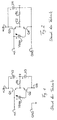
- the known complementary amplifier of Fig. 1 includes in series an NPN transistor Q1 and a pnp transistor Q2 between two voltage terminals + Ub and -Ub, which are fed by two series-connected voltage sources V2, V3.
- the connection node of these voltage sources is at the ground potential GND connected and connected to a terminal of the load RL.
- the other connection of this load RL is located at the connection node of the two transistors Q1, Q2.
- For the Closed-circuit current setting of the two transistors Q1, Q2 provides an adjustable Bias source Vbias between the two bases of these transistors.
- Vbias can be the quiescent current of the two Set transistors to be e.g. each working in AB amplification mode.
- the unbalanced input voltage is via an input + in the base of the npn transistor fed.
- the complementary amplifier is remote with respect to the mass Non-inverting load connection. Capacitors for potential separation are shown in FIG. 1 not shown. In any case, they are necessary if the input signal has a DC voltage is superimposed and the input voltage swing is not very large to the base-emitter voltage of transistor Q1.
- the known complementary amplifier according to Fig. 2 requires in contrast to Fig. 1 only a voltage source V4 for the two series-connected complementary transistors Q3, Q4 of an npn and a pnp transistor between a positive Supply terminal + Ub and the ground terminal GND lie.
- the voltage source V4 is GND with its one connection to ground and feeds the other one Supply connection + Ub.
- the quiescent current setting for the two transistors takes place as in Fig. 1 via an adjustable bias source Vbias, between the two Basic connections is. Since the common emitter terminal in this complementary circuit Also approximately no longer lies on the ground potential GND, there is in the Idle state a voltage difference between the common emitter terminal and the ground GND, which corresponds to about half the supply voltage V4.
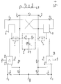
- Fig. 3 shows that described in the already mentioned U.S. Patent US 4,229,706 Audio balanced amplifiers with symmetrical construction, which are in the two signal paths DC-coupled and whose two NPN output stage transistors Q1, Q2 each of a floating power supply V1, V2 are powered.
- the galvanic isolation from the ground reference potential GND is at the floating power supply usually by means of its own power transformer and a bridge rectifier circuit reached.
- the load RL is connected between the two emitters, the also the base points for the cross-connected floating supply voltages V1, V2 form.
- the balanced input signal is sent through the inputs + in and -in, the positive input being + in with the noninverting input connected in bipolar operating amplifier U1 is connected.
- the negative input -in is with the non-inverting input one to the first Operational amplifier U1 identical second operational amplifier U2 connected.
- the Output of the first or second operational amplifier is direct, ie without coupling capacitor, is connected to the base of the first and second output transistors Q1, Q2, respectively.
- the power supply of the two operational amplifiers via two in Series connected voltage sources V3, V4, whose point of connection to the ground potential GND is connected and whose mass-remote poles the positive and negative supply voltage + V, -V for the two operational amplifiers U1, U2 form.
- the quiescent current adjustment of the two output transistors Q1, Q2 takes place via in each case a resistor R4 or R5 between the emitter and the negative Supply voltage -V.
- the corresponding base current supplies the output of the associated operational amplifier U1 or U2.
- the current determined by the resistor R4 or R5 must be identical to that of the Operational amplifier U1 or U2 supplied base current, since this current only with the voltage sources V3, V4 is linked and no other current path available stands. So it is not regulated the emitter quiescent current, but the base current.
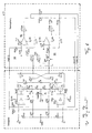
- Fig. 4 shows schematically the circuit diagram of a first embodiment of a balanced push-pull amplifier according to the invention.
- the two signal paths are symmetrically constructed and each contain a preamplifier block N1B and N2B and a power amplifier M1 and M2, respectively.
- the power amplifiers M1, M2 are each connected to one floating power supply V1, V2 connected, with the load circuits via a load RL, which is between the bases of the two power amplifiers M1, M2 is connected, are crossed over.
- the two bases of the power amplifier At the same time set the connection points or terminals RL1, RL2 for the externally connected load RL and form the signal output.
- the power supply of the preamplifier blocks N1B, N2B contains at least two series-connected voltage sources V3, V4, their connection point to ground GND is.
- the resulting supply voltages + Ub and -Ub feed the supply terminals of the preamplifier blocks, which in the embodiment of FIG. 4 each from an input side amplifier N1, N2 with high open-loop gain consist.
- the positive pole of the output stage of the amplifiers N1, N2 is positive Supply voltage + Ub or with another positive and also supplied ground-based voltage source.
- the negative pole of the output stage of the Amplifier N1, N2 is connected via a potential difference generator 4, 5 with the associated Load connection RL1, RL2 connected. About this potential difference generator 4, 5 flows an impressed current.
- the amplifier N1, N2 Due to the high idling gain in conjunction with a high-impedance non-inverting and high-impedance inverting input, with negligible offset voltage and negligible offset current and with a low-impedance output, the amplifier N1, N2 have a behavior like a more or less ideal op amp.
- the first power amplifier M1 is of a floating first Voltage source V1 and the second power amplifier M2 is a floating second voltage source V2 fed.
- the first power amplifier M1 is over its first supply terminal with a pole of the first voltage source V1 and over its second supply terminal, which also serves as a power amplifier output, with the first output RL1 and the load RL with the other pole of the first Voltage source V1 connected.
- the second power amplifier M2 is over its first Supply terminal with a pole of the second voltage source V2 and via its second supply terminal, which also serves as a power amplifier output, with the second output RL2 and via the load RL to the other pole of the second Voltage source V2 connected,
- the required operating point-determining control voltage is in the associated Potential difference generators 4, 5 by one of a quiescent current setting Ix determined with an adjustable current source I1 predetermined current, over the Potential difference generator 4, 5 generates the desired potential offset.
- the with the negative supply connection -Ub connected quiescent current setting device Ix contains an adjustable current source I1, whose current by means of the two with the Output terminals RL1, RL2 connected resistors R2, R3 in half on the two Potential difference generator 4, 5 is divided, so that the operating point setting for the two power amplifiers M1, M2 takes place symmetrically.
- this adjustment process can be done in different ways, For example, purely manually as in the embodiment of Fig. 4 via an adjustable Current source I1, an adjustable voltage source Vbias (see Fig. 8) or via a Potentiometer that controls the current source I1. It is also useful temperature-sensitive control, which has a temperature sensor that determines the temperature detected at least one power component, the adjustable current or Voltage source I1 or Vbias influenced so that the quiescent current of Power components of the power amplifier M1, M2 remains constant or one having predetermined temperature profile.
- the two amplifiers N1 and N2 have one inverting and one non-inverting one Input and correspond due to their high idle gain each one Operational amplifier.
- the load connection RL1 or RL2 which by a Feedback network is regulated to the ground potential GND.
- the Feedback network is through the series-connected resistors R6 and R7 or R8 and R9 formed between the load terminal RL1 and ground GND and the Load connection RL2 and ground GND are.
- the common connection point of the Resistors R6, R7 and R8, R9 is connected to the inverting input of the amplifier N1 or N2 connected.
- the non-inverting input of the first amplifier N1 is with the positive signal input + in and the non-inverting input of the second Amplifier N2 is connected to the negative signal input -in the push-pull amplifier connected.
- R6, R7 and R8, R9 is the output of the amplifier N1 or N2 regulated so that via the potential difference generator 4, 5 and the voltage divider R6, R7 and R8, R9 the potential at the non-inverting Input of the amplifier N1 or N2 identical to the potential at the positive or negative Signal input + in or -in is.
- This regulation over the feedback network is regardless of the size of the quiescent current setting for the power components of Power amplifier M1, M2, which is predetermined by the adjustable current source I1.
- the resulting level offset at the potential difference generator 4 and 5 is determined by the Amplifier N1 or N2 regulated.
- the resistors R10 and R11 from the positive and negative signal input to ground GND have no meaning for the feedback. They are only for determination the GND potential for the respective noninverting inputs of N1 and N2 and the line adaptation, since the signal inputs to the noninverting Inputs of amplifiers N1 and N2 are usually high impedance. Later will be one Embodiment shown in which the signal inputs to the inverting inputs the amplifiers N1 and N2 are connected. By the to these inputs connected feedback network, these inputs are then essential low impedance, so that a line adjustment may be omitted if necessary.
- the upper amplifier half essentially of the modules N1B and M1 consisting amplifies the one half-wave of the balanced input signal and the lower amplifier half, consisting of the modules N2B and M2, amplifies the another half wave.
- the power amplifiers M1, M2 can be practically implemented in a variety of ways: as individual power devices such as e.g. Power MOSFETs, IGBTs or bipolar Power transistors, but also advantageous combinations of the same or various amplifier components with or without local negative feedback.
- individual power devices such as e.g. Power MOSFETs, IGBTs or bipolar Power transistors, but also advantageous combinations of the same or various amplifier components with or without local negative feedback.
- the output stage of the preamplifier blocks N1B and N2B exemplified as triode Xtr1 or Xtr2 executed.
- the preamplifier blocks N1B and N2B each consist of the combination of a input side amplifier N1, N2 with high open-loop gain and one to the Amplifier N1, N2 connected tube Xtr1, Xtr2, whose control grid with the associated amplifier output is connected.
- the anode of the tube Xtr1, Xtr2 is with the positive supply voltage + Ub or with another positive and also mass-related voltage source connected.
- the cathode of the tube Xtr1, Xtr2 is over a potential difference generator 4, 5, which in the simplest case a resistor R4, R5 contains and over which an impressed current flows, with the associated load connection RL1, RL2 connected.
- tubes Xtr1, Xtr2 shown as triodes in the embodiment of FIG Of course, tetrodes, pentodes, hexodes and heptodes with the state of Technology corresponding wiring of the additional grid can be used.
- Fig. 5 As power amplifier M1, M2, two n-channel MOSFETs are shown in Fig. 5, whose respective gate electrode to the cathode of the preceding tube Xtr1, Xtr2 connected.
- the respective source electrode is connected to the associated load connection RL1, RL2 and the respective drain electrode with the positive potential of floating voltage source V1, V2 connected.
- the operating point-determining gate-source control voltage is in the associated potential difference generators 4, 5 by one of a quiescent current setting device Ix with an adjustable current source I1 predetermined current determined by the resistors R4, R5 the desired Potential offset generated.
- the one connected to the negative supply terminal -Ub Quiescent current adjuster Ix contains an adjustable current source I1 whose current by means of the two resistors connected to the output terminals RL1, RL2 R2, R3 is split in half on the two resistors R4, R5, so that the Operating point setting for the two MOSFETs M1, M2 takes place symmetrically.
- Fig. 5 is schematically such a control arrangement as "Biasregelung" B1, which complements the push-pull amplifier of Fig. 4. Same thing Circuit and functional units in all figures of the drawing with the same Reference signs are provided, unnecessary repetitive descriptions of functions.
- the circuit block B1 contains two control circuits B2, B3 whose inputs are connected to the Amplifier outputs RL1, RL2 and their outputs with the feedback networks the two preamplifier blocks N1B and N2B are coupled.
- the input of the first control circuit B2 is equal by two connected in series Resistors R16, R17 are formed, which are connected to the outputs RL1, RL2 and their common connection point avg via a resistor R15 on the inverting input of an operational amplifier U3 is connected.
- a DC voltage V5 is applied at the non-inverting input of U3, a DC voltage V5 is applied.
- the exit of the amplifier U3 is by means of a capacitor C2 to the non-inverting Entrance returned.
- the power supply of the amplifier U3 takes place expediently via the already existing supply potentials + Ub and -Ub or via another supply voltage.
- the input of the second control loop B3 is formed by a subtractor D1, whose Minuendeingang + with the load terminal RL2 and its Subtrahendeingang - is connected to the load terminal RL1.
- the output of the subtracter D1 determines the potential of the node is diff and is connected to the inverting resistor R14 Input of an amplifier U4 connected via a capacitor C1 with his Amplifier output is connected. This output is also via a series circuit from an inverter N4 and a resistor R12 to the circuit node bias 1 and connected via a resistor R13 to the other circuit node bias 2.
- At the non-inverting input of the amplifier U4 is the ground potential GND connected.
- control block bias control B1 The function of the control block bias control B1 according to the invention is to that by means of the first control loop B2, the mean value avg of the potentials at the Outputs RL1, RL2 detected and compared with a predetermined target voltage V5 becomes.
- About the integrator formed by the amplifier U3 is the deviation of Potential avg amplified from the setpoint V5.
- the two directly coupled rule interfaces bias 1 and bias 2 indicate that the Average of the potentials at the output terminals RL1, RL2 to the predetermined Setpoint V5 is adjusted. This will be the magnitude of the absolute potential of the outputs RL1, RL2 defined set.
- ⁇ 2 greater than or equal to 1s makes sense.
- the amplifiers N1 or N2 in the preamplifier blocks realized so that in Hibernation a significant, also driftbelasteter, potential difference between the noninverting and the inverting input of these amplifiers N1, N2 occurs, so can by means of a suitable design of the bias control this disturbing influence on the Working point stability can be minimized.
- the first stage of a tube amplifier could be realized as a cathode base stage.
- the grid corresponds to the non-inverting input of the amplifier N1 or N2 and the cathode corresponds to the inverting input of N1 or N2.
- the operating points of tubes are thermal and aging-related fluctuations subjected. This changes the temperature and the aging of the input tubes, essentially the voltage gain in the amplifiers N1 and N2 cause the current component I (R6) or I (R8), and thus after the first relationship the by I (R4) certain potential of the gate-source path of the power amplifier M1. Accordingly, the potential determined by the current I (R5) has a negative effect on the Gate-source path of the power amplifier M2 off. To this disturbing influence to exclude or at least minimize the target voltage V5 is not fixed set, but as in the embodiment of Fig.
- These Node voltage avgln is connected through a resistor R26 to the noninverting Input of the control amplifier U3 out, the unlike in Fig. 5 not with a Reference voltage V5 is fed, but its reference voltage at this Connection itself generated by a capacitor C3 is connected there.
- bias 1 and bias 2 is thus over the RC element R26 and C3 low-pass filtered and then serves as a target voltage on non-inverting input of the control amplifier U3.
- the corner frequency of the RC element R26, C3 is preferably at least one decade lower than the lowest to be transferred Payload frequency selected.
- this circuit variant shown in Fig. 6 is the fundamental or drift - related potential difference between the inputs of the Amplifier N1 or N2, on the negative feedback network part of the Output voltage is returned, and the output node RL1 or RL2 ideal to Zero regulated or at least so small that with it the error portion of the Closed-circuit current control has no influence.
- FIG. 7 an embodiment of the push-pull amplifier is shown, as Power amplifiers M1, M2 each have tubes Xtr3, Xtr4, which directly drive the load RL.
- the preamp blocks N1B, N2B contain, unlike the previous ones Embodiments of FIG. 5 and FIG. 6 no combination amplifier, but consist solely of the amplifiers N1, N2. These are so realized that they are in the Hibernate a negative DC output voltage from a few volts to a few tens Volts depending on the connected tubes Xtr3, Xtr4 have.
- the adjustable Current source I1 is connected to a positive potential + Ub, so that half their Current through the resistors R2, R3, the level shifters 4, 5 and the internal Output stage from N1, N2 to negative supply voltage -Ub flows.
- This Current flow causes the necessary negative ones at the resistors R4, R5 Grid bias for tubes Xtr3 and Xtr4. It will be back with only one Control value of the quiescent current of both tubes Xtr3, Xtr4 in the floating without fixed Ground reference powered amplifiers M1, M2 defined and synchronous as well set symmetrically.
- the load RL in a special case by means of a transformer to the with Tubular equipped power amplifier M1, M2 can be coupled with the the same structure as in Fig. 7, except that then instead of the direct load coupling a transformer in a known manner to the internal resistance of the tube output stage the low-impedance load stepped down.
- the transformer can save costs be executed as autotransformer, since by the inventive Closed-circuit current setting no DC bias occurs.
- the autotransformer is wound symmetrically, for example in a two-chamber design, so that the same winding resistances result for both winding halves. Due to the lack of DC biasing is also a realization as a toroidal transformer possible.
- the winding will be the same as an integer Split parts, which are then wrapped in pairs bifilar.
- Symmetry principle for example, by simply winding up the respective Windings, still allows a stable operation of the invention Push-pull amplifier, but does not fully exploit its possibilities.
- FIG. 8 Another embodiment of the push-pull amplifier according to the invention shows Fig. 8.
- This circuit is almost identical to the circuit of Fig. 6, except that the Control value for the quiescent current setting not as in Fig. 6 by the adjustable Current source I1, but by an adjustable voltage source Vbias, the Ultimately via the resistors R2, R3 but also generates a current that means these resistors R2, R3 is divided in half and the resistors R4, R5 the desired operating point determining potential offset for the respective gate-source path of the two n-channel MOSFETs in the power amplifier M1, M2 generated.
- the absolute value of the potentials at the load terminals RL1, RL2 defined and adjusted to an approximately equal value. Since the resistors R2 and R3 are equal to each other, are also the flows flowing through them I (R2) and I (R3) equal to each other. These currents flow almost completely across the resistors R4 or R5 and from the cathode to the anode of the triode Xtr1 and Xtr2 to the positive Operating voltage + Ub. Due to the resulting potential offset on the resistors R4 or R5 becomes a defined positive potential difference between the gate-source path the MOSFETs M1 and M2 generated and thus flows logically a defined Quiescent current through these output stage transistors.
- the adjustment process of the voltage source Vbias can again be done in a variety of ways, manually, temperature controlled or by means of an automatic quiescent current control circuit.
- a push-pull amplifier according to the invention can also be realized by the input side amplifiers N1, N2 in the Pre-amplifier blocks N1B, N2B each with their inverting amplifier input on the signal inputs -in and + are connected in the push-pull amplifier.
- the input side amplifiers N1, N2 in the Pre-amplifier blocks N1B, N2B each with their inverting amplifier input on the signal inputs -in and + are connected in the push-pull amplifier.
- in the Input range of the amplifiers N1, N2 are only minor Make circuit changes.
- the resistors R7 and R9 of Feedback networks are now not connected to the ground potential as For example, in the comparable Fig. 5, but to the negative or positive Signal input -in or + in the push-pull amplifier.
- the resistors R10 and R11 on The non-inverting inputs of the amplifiers N1 and N2 are connected to the from the Amplifier opposite ends connected to the ground potential GND. Furthermore, the recirculated lines of the rule interfaces bias 1 and 2 bias no longer as in Fig.5 fed back to the inverting input of the amplifier N1 or N2, but on their non-inverting inputs. The recirculated from the control circuits B2 and B3 Control currents generate the necessary via the resistors R10 and R11 Control voltages for the amplifiers N1, N2.
- FIG. 10 shows a further variant of the quiescent current setting.
- the basic circuit of this push-pull amplifier is roughly comparable to the Circuit of Fig. 5.
- the potential difference generator 4 and 5 contain in addition to the Resistors R4 and R5 are each an optoelectronic device OK1 or OK2 or are coupled with such devices. Via a common current source I1 controlled the light emission of each one LED element, the intensity of which Volume resistance of a photosensitive photo-transistor is dependent.
- This Photo transistor is parallel to the already known from Fig. 5 resistor R4 or R5, which is fed via the likewise known resistor R2 or R3, whose Base point but in contrast to Fig. 5 on the negative fixed potential -Ub.
- the potential difference generators 4 and 5 respectively Thus formed by an assembly, the resistors R4 and R5 each with a Optokopplerrank OK1 or OK2 combined.
- a synchronous setting of the Quiescent current of both branches of the floating voltage supplied power amplifier takes place by the application of both optocouplers with the same control or Control current.
- the current equality is in the embodiment of FIG. 10 thereby forced, that the current of the adjustable current source I1 from the negative Supply connection -Ub through both optocouplers OK1, OK2 until positive Supply connection + Ub is looped through.
- the exemplary embodiment according to FIG. 11 shows an advantageous arrangement of the push-pull amplifier according to the invention when basically only unbalanced input signals are to be processed instead of symmetrical input signals.
- the circuit according to FIG. 5 is suitable.
- the amplifier N1 at the non-inverting input and the amplifier N2 at the inverting input are driven.
- the non-inverting input of the amplifier N1 is connected to the signal input + in and via the resistor R10 to the ground potential GND.
- the inverting input of the amplifier N1 is located at the voltage tap of the voltage divider R6, R7, as in FIG.
Abstract
Description
Die wesentlichen Qualitätskriterien für Leistungsverstärker, insbesondere bei Anwendungen im Audiobereich, sind ein möglichst geringer Klirrfaktor, eine hohe Bandbreite, ein möglichst geringer Innenwiderstand, möglichst geringe transiente Intermodulationsverzerrungen und eine hohe Arbeitspunktstabilität der Leistungsbauelemente.The main quality criteria for power amplifiers, especially at Applications in the audio sector, are as low as possible harmonic distortion, high Bandwidth, the lowest possible internal resistance, the lowest possible transient Intermodulation distortions and a high operating stability of the Power devices.
Leistungsverstärker können mit sehr unterschiedlichen aktiven Bauelementen aufgebaut werden, deren Eigenschaften in der Regel die Struktur des Verstärkers bestimmen: Röhren mit unterschiedlichem Aufbau, z.B. Trioden, Tetroden, Pentoden, oder Halbleiterbauelemente, z.B. Bipolartransistoren, Feldeffekttransistoren, MOSFETs und IGBTs. Röhren haben für den Einsatz als Leistungsverstärker in der Regel einen vergleichsweise hohen Innenwiderstand und müssen deshalb mit Hilfe von speziell aufgebauten Transformatoren, den Übertragern, an die niedrige Impedanz des Lautsprechers angepasst werden. Diese Übertrager begrenzen indessen die erzielbare Bandbreite und sind selbst Quelle erheblicher nichtlinearer Verzerrungen. Die deshalb wünschenswerte direkte Ankopplung der in der Regel niederohmigen Last des Lautsprechers erfordert die Verwendung von aktiven Bauelementen mit möglichst geringem Innenwiderstand bzw. möglichst großer Steilheit. Aus diesem Grund hat sich als Stand der Technik die Verwendung von Halbleiterbauelementen wie Bipolartransistoren, MOSFETs oder in selteneren Fällen auch IGBTs durchgesetzt.Power amplifiers can be built with very different active components whose properties usually determine the structure of the amplifier: Tubes of different construction, e.g. Triodes, tetrodes, pentodes, or Semiconductor devices, e.g. Bipolar transistors, field effect transistors, MOSFETs and IGBTs. Tubes usually have one for use as a power amplifier comparatively high internal resistance and therefore must with the help of special constructed transformers, the transformers, to the low impedance of the Speaker can be adjusted. These transformers, however, limit the achievable Bandwidth and are themselves the source of significant nonlinear distortions. That's why Desirable direct coupling of the usually low-impedance load of Speaker requires the use of active components as possible low internal resistance or steepest possible. That's why As prior art, the use of semiconductor devices such as bipolar transistors, MOSFETs or, more rarely, IGBTs.
Besonders häufig werden Verstärker mit höheren Leistungsanforderungen als komplementäre Gegentaktverstärker realisiert, wobei komplementäre Bipolartransistoren (npn- und pnp-Transistor) oder komplementäre MOSFETs (n-Kanal- und p-Kanal-Transistor) oder komplementäre IGBTs (n-Kanal- und p-Kanal-Typ) mit einer auf Massepotential bezogenen bipolaren oder unipolaren Betriebsspannungsquelle eingesetzt werden.Particularly frequent are amplifiers with higher performance requirements than complementary ones Push-pull amplifier realized, whereby complementary bipolar transistors (npn- and pnp transistor) or complementary MOSFETs (n-channel and p-channel transistors) or complementary IGBTs (n-channel and p-channel type) with a ground potential related bipolar or unipolar operating voltage source can be used.
Das gemeinsame Merkmal des in Fig. 1 und Fig. 2 dargestellten Prinzips eines typischen halbleiterbestückten Gegentaktverstärkers oder einer entsprechenden Gegentaktendstufe ist die Verwendung eines komplementären Transistorpaares. Zur Ruhestromeinstellung über das komplementäre Transistorpaar dient eine einstellbare Vorspannungsquelle, die zwischen den beiden Basisanschlüssen des komplementären Transistorpaares liegt. Die weiteren Schaltungsteile sind dann zueinander unterschiedlich.The common feature of the principle illustrated in FIG. 1 and FIG Semi-conductor push-pull amplifier or a corresponding push-pull output stage is the use of a complementary transistor pair. To quiescent current setting via the complementary transistor pair is an adjustable bias source, the lies between the two base terminals of the complementary transistor pair. The other circuit parts are then different from each other.
In der Grundschaltung von Fig. 1 werden im Leistungsteil mindestens zwei in Reihe geschaltete Spannungsquellen verwendet, deren Verbindungspunkt an Masse gelegt ist, so dass sich bezogen auf das Massepotential eine positive und eine negative Versorgungsspannung ergibt. Das Ansteuersignal ist ein auf Massepotential bezogenes symmetrisches Signal. Die Last, z.B. der Lautsprecher, liegt zwischen dem Verbindungspunkt des komplementären Transistorpaares und dem Masseanschluss.In the basic circuit of Fig. 1, at least two in series in the power section switched voltage sources whose connection point is grounded, so that in relation to the ground potential one positive and one negative Supply voltage results. The drive signal is related to ground potential symmetrical signal. The load, e.g. the speaker, lies between the Connection point of the complementary transistor pair and the ground terminal.
In der Grundschaltung von Fig. 2 wird im Leistungsteil nur eine einzige Spannungsquelle mit einseitigem Masseanschluss verwendet. Das Ansteuersignal ist ein auf Massepotential bezogenes unipolares Signal. Wenn die Last einen Gleichstrompfad aufweist, muss sie kapazitiv von den auf unterschiedlichen Pegeln liegenden Ausgangsklemmen, die durch den Verbindungspunkt des komplementären Transistorpaares und den Masseanschluss gebildet sind, getrennt werden.In the basic circuit of Fig. 2 in the power section only a single voltage source used with single sided ground connection. The drive signal is on Ground potential related unipolar signal. When the load is a DC path it must be capacitive from those at different levels Output terminals through the connection point of the complementary Transistor pair and the ground terminal are formed, to be separated.
Am zuletzt genannten Merkmal ändert sich auch nichts wesentliches durch das Einfügen eines sehr niederohmigen Messwiderstandes zwischen dem Lastwiderstand bzw. dem Lautsprecher und der Masse, wie dies in einigen Publikationen zur Strommessung vorgeschlagen wird.The latter feature also does not change anything essential to the insertion a very low-impedance measuring resistor between the load resistor or the Speakers and the mass, as in some publications for current measurement is proposed.
Komplementäre Gegentaktendstufen mit Röhren gibt es nicht, da Röhren entsprechend dem Elektronenfluss zwischen Kathode und Anode nur einen negativen Strom steuern, so dass ein zur Elektronenröhre komplementäres Verstärkerelement fehlt.Complementary push-pull power amplifiers with tubes do not exist, as tubes do accordingly control the flow of electrons between cathode and anode only a negative current, so that an amplifier element complementary to the electron tube is missing.
Für die Realisierung hochlinearer Leistungsverstärker wäre der Einsatz von Röhren als
Spannungsverstärker jedoch sehr wünschenswert, da in diesem Anwendungsfall Röhren
wegen ihrer quadratischen Strom-Spannungskennline sehr verzerrungsarm betrieben
werden können. Optimal wäre die Kombination von Röhren als Spannungsverstärker mit
hochsteilen Halbleiterbauelementen, wie Bipolartransistoren, MOSFETs oder IGBTs, als
ausgangsseitiger Leistungsverstärker. Von großem Vorteil wäre hierbei eine
Gleichstromkopplung zwischen den einzelnen Verstärkungsstufen, damit die ansonsten
für die Potentialtrennung erforderlichen Kopplungs- oder Überbrückungskondensatoren
oder Übertrager keinen schädlichen Einfluss auf den Frequenzgang oder den Klirrfaktor
haben.
Die bisherigen Entwicklungen konzentrierten sich auf die Optimierung von reinen
Transistorverstärkern einerseits und reinen Röhrenverstärkern andererseits. Daneben
sind auch vereinzelt Verstärker mit hybrider Bauelementebestückung bekannt, die
getrennt nach Röhren- bzw. Transistorverwendung optimierte Vor- und
Leistungsverstärker enthalten, die in der Regel kapazitiv miteinander gekoppelt sind.For the realization of highly linear power amplifiers, however, the use of tubes as a voltage amplifier would be very desirable, since in this application, tubes can be operated very low distortion because of their square current-voltage characteristic. Optimal would be the combination of tubes as a voltage amplifier with hochsteil semiconductor devices, such as bipolar transistors, MOSFETs or IGBTs, as output side power amplifier. Of great advantage here would be a DC coupling between the individual amplification stages, so that the coupling or bypass capacitors or transformers otherwise required for the potential separation have no detrimental effect on the frequency response or harmonic distortion.
The developments so far concentrated on the optimization of pure transistor amplifiers on the one hand and pure tube amplifiers on the other hand. In addition, occasionally amplifiers with hybrid component assembly are known, which contain separately after tube or transistor use optimized pre and power amplifiers, which are usually capacitively coupled together.
Bei den komplementären Gegentaktendstufen gemäß Fig. 1 mit den beiden auf Massepotential bezogenen Spannungsquellen entgegengesetzter Polarität führt die Verwendung von komplementären aktiven Bauelementen im Leistungsteil zwangsläufig zu einer inhärent nichtsymmetrischen Struktur. So sind beide Zweige des im Gegentakt arbeitenden Verstärkers nicht mit den gleichen Bauelementen aufgebaut und damit prinzipiell nur bedingt symmetrisch. Die volle elektronische Symmetrie würde erfordern, dass bis auf den Leitungstyp alle elektronischen Eigenschaften des npn- und pnp-Transistors einander gleich sind. Das ist natürlich nur näherungsweise erreichbar. Die Unterschiede stören das Symmetrieverhalten der Verstärkung in den beiden Signalpfaden und erschweren u.a. die Realisierung weiterer verzerrungsmindernder Schaltungsstrukturen.In the complementary push-pull output stages shown in FIG. 1 with the two on Ground potential related voltage sources of opposite polarity leads the Use of complementary active components in the power unit inevitably to an inherently nonsymmetrical structure. So both branches are in push-pull working amplifier not built with the same components and thus in principle only conditionally symmetrical. Full electronic symmetry would require that all the electronic properties of the npn and pnp transistors except for the line type are equal to each other. Of course this is only approximate. The Differences disturb the symmetry behavior of the gain in the two Signal paths and complicate u.a. the realization of further distortion reducing Circuit structures.
Ein Problem bei der Suche nach einem möglichst symmetrischen komplementären Transistorpaar ist die sehr begrenzte Auswahl an pnp-Bipolartransistoren, p-Kanal-MOSFETs und p-Kanal-IGBTs für hochwertige Leistungsverstärker. Dieses Problem wird durch den Aufbau einer quasikomplementären Leistungsstufe nicht behoben, sondern auf Kosten der Symmetrie nur in die Treiberstufe verlagert. Die in der Realität verwendbaren Paare komplementärer Transistoren sind bei näherer Analyse keineswegs echte Paare. So unterscheiden sich die komplementären Transistoren eines Komplementärpaares zum Beispiel maßgeblich hinsichtlich des Betrages des Stromverstärkungsfaktors bei Bipolartransistoren bzw. der Steilheit bei MOSFETs und IGBTs. Dies ist eine wesentliche Ursache für Nichtlinearitäten im Verstärkerverhalten.A problem in the search for a symmetrical as possible complementary Transistor pair is the very limited range of pnp bipolar transistors, p-channel MOSFETs and p-channel IGBTs for high quality power amplifiers. This problem will not resolved by building a quasicomplementary performance level, but on Costs of symmetry only shifted to the driver stage. The usable in reality Pairs of complementary transistors are by no means real pairs on closer analysis. Thus, the complementary transistors of a complementary pair differ from each other Example relevant to the amount of current amplification factor in bipolar transistors or the slope in MOSFETs and IGBTs. This is an essential one Cause for nonlinearities in the amplifier behavior.
Beispielsweise ist bei gleicher Drain-Source-Spannungsfestigkeit, gleichem zulässigen maximalen Drainstrom sowie gleicher maximal zulässiger Verlustleistung die Chipgröße von p-Kanal-MOSFETs ca. dreimal größer als die Chipfläche des komplementären n-Kanal-MOSFETs. Das führt zwangsläufig zu erheblich unterschiedlichen Kapazitäten, insbesondere der Gate-Source-Kapazität und der Drain-Source-Kapazität. Durch die unterschiedlichen kapazitiven Lasten resultieren Probleme bei der Ansteuerung und ohne weitere Schaltungsmaßnahmen ergeben sich unterschiedliche Flankensteilheiten (= Slew-Rate) für positive und negative Flanken am Verstärkerausgang. Wird ein solcher Verstärker gegengekoppelt, wird die Frequenzkompensation von den erheblich größeren Kapazitäten des negativen Zweiges (p-Kanal MOSFETs bzw. -IGBTs) bestimmt. Das kann die erreichbare Leistungsbandbreite unzulässig stark reduzieren oder zu Instabilitäten führen. Bei Bipolartransistoren sind diese Anpassprobleme (=Matching-Probleme), die für die komplementäre Symmetrie erforderlich sind, ähnlich.For example, with the same drain-source withstand voltage, the same permissible maximum drain current and the same maximum allowable power dissipation the chip size of p-channel MOSFETs about three times larger than the chip area of the complementary n-channel MOSFETs. This inevitably leads to significantly different capacities, in particular the gate-source capacitance and the drain-source capacitance. By the different capacitive loads result in problems with the control and without Further circuit measures result in different edge steepnesses (= Slew rate) for positive and negative edges at the amplifier output. Will one Amplifier negative feedback, the frequency compensation of the considerably larger Capacitance of the negative branch (p-channel MOSFETs or -IGBTs) is determined. The can unduly reduce or increase the achievable power bandwidth Lead instabilities. In bipolar transistors, these matching problems (= matching problems), which are required for the complementary symmetry, similar.
Zusammenfassend ist festzustellen, dass die dem Stand der Technik entsprechenden Gegentaktverstärker in Komplementärtechnik prinzipbedingt keine vollständige Symmetrie erreichen können. Es sind einige Verfahren bekannt, welche die daraus resultierenden Nichtlinearitäten mittels einer Gegenkopplung und/oder einer Vorwärtsfehlerkompensation (= Forward-Error-Correction) zu beheben versuchen. Der dafür notwendige Schaltungsaufwand ist für hochqualitative Leistungsverstärker allerdings sehr hoch. Desweiteren ist die korrekte Arbeitsweise der Fehlerkompensation bei der für Audio-Anwendungen typischen Ansteuerung mit transienten Impulsen kritisch. So ist beispielsweise in der US Patentanmeldung US 5,892,398 ein Leistungsverstärker beschrieben, der vom Ausgangssignal gesteuerte Betriebsspannungen nach dem Bootstrap-Prinzip für die Kompensationsbaugruppe verwendet, deren hochlineare Erzeugung wiederum schwierig ist. Der für Audio-Leistungsverstärker typische Fall der Ansteuerung komplexer, auch kapazitiver Lasten wie Lautsprecher und Frequenzweichen unterschiedlichster Bauart, erfordert eine hohe Stabilität im gegengekoppelten Zustand, die mit herkömmlichen komplementären Gegentaktendstufen auf Grund der unterschiedlichen Hochfrequenzeigenschaften beider Signalpfade nur eingeschränkt erreichbar ist.In summary, it should be noted that the state of the art Push-pull amplifiers in complementary technique inherently not complete Can achieve symmetry. There are some known methods which are the result resulting non-linearities by means of negative feedback and / or forward error compensation (= Forward-Error-Correction) try to fix. The one for it However, the necessary circuitry is very important for high-quality power amplifiers high. Furthermore, the correct operation of the error compensation in the for Audio applications typical control with transient pulses critical. So is For example, in US Patent Application US 5,892,398 a power amplifier described, the output voltages controlled by the output after the Bootstrap principle used for the Kompensationsbaugruppe whose highly linear Generation is difficult. The case of the audio power amplifier typical of Control of complex, even capacitive loads such as loudspeakers and crossovers of the most varied design, requires a high stability in the counter-coupled state, those with conventional complementary push-pull output stages due to the different high-frequency characteristics of both signal paths only limited is reachable.
Übertragerlose Gegentaktleistungsverstärker, die aktive Bauteile nur eines Leitfähigkeitstyps verwenden und die damit streng symmetrisch bezüglich der elektrischen Eigenschaften realisierbar sind, wurden bislang insbesondere mit Röhren auf den Markt gebracht. Sie werden allgemein als OTL-Verstärker bezeichnet (= Output Transformer-Less) und unter dieser Bezeichnung kommerziell angeboten. Röhrenverstärker, die nach diesem Prinzip gebaut sind, weisen folgende grundsätzlichen Nachteile auf: Röhren haben eine zu geringe Steilheit, um die niederohmige Impedanz des Lastwiderstandes bzw. des Lautsprecher direkt anzusteuern. Ohne weitere Schaltungsmaßnahmen resultieren hieraus eine geringe abgebbare Leistung und ein sehr hoher Klirrfaktor.Transformerless push-pull power amplifiers, the active components only one Use conductivity type and thus strictly symmetrical with respect to electrical properties are realized, have been so far especially with tubes brought the market. They are commonly referred to as OTL amplifiers (= output Transformer-Less) and commercially available under this name. Tube amplifiers built according to this principle have the following basic features Disadvantages on: Tubes have a too low slope to the low impedance of the Direct load or the speaker directly to control. Without further Circuit measures result from this a low deliverable performance and a very high harmonic distortion.
Um die Steilheit zu erhöhen, werden viele Röhrensysteme parallel geschaltet. Damit lässt sich bei exzessiv parallel geschalteten Röhren bzw. Röhrensystemen die Steilheit des daraus resultierenden Leistungsbauelementes auf einen gerade ausreichenden Wert erhöhen. Der Klirrfaktor bleibt aber immer noch hoch. Es gibt nun aber erhebliche Probleme mit der Stabilität der Arbeitspunkte der vielen Röhrensysteme. Die thermische Drift des Anodenstromes bei vorgegebener Gittervorspannung und die Änderung der Röhreneigenschaften infolge von Alterung, wie z.b. nachlassende Katodenemissionsfähigkeit, führen im günstigsten Fall zu einem erhöhten Klirrfaktor, im ungünstigsten Fall zum Totalausfall des Gerätes.To increase the steepness, many tube systems are connected in parallel. Leave it In excessively parallel connected tubes or tube systems, the steepness of the resulting power component to a just sufficient value increase. The harmonic distortion is still high. But there are significant ones now Problems with the stability of the working points of many tube systems. The thermal Drift of the anode current at a given grid bias and the change of Tube properties due to aging, such as. declining Katodenemissionsfähigkeit lead in the best case to increased harmonic distortion, in worst case total failure of the device.
Der Arbeitspunkt der Leistungsstufe wird bei diesen Röhrenschaltungen mittels einer festen Gittervorspannung wie beispielsweise im US-Patent 4,719,431 oder durch je einen Katodenwiderstand eingestellt. Die zugehörige Vorstufe bzw. der Spannungsverstärker wird kapazitiv angekoppelt. Beispiele hierfür zeigen die US-Patente US 4,719,431 in Fig.4 und US 6,242,977 B1 in Fig.2. Eine Gleichspannungskopplung ist nach dem Stand der Technik nur indirekt mittels eines hochohmigen Spannungsteilers möglich, der wiederum kapazitiv überbrückt werden muss. Ohne diesen Überbrückungskondensator wäre der Wechselspannungsabfall viel zu groß. Andererseits würde eine direkte Gleichspannungskopplung den ohnehin schon stark driftgefährdeten Arbeitspunkt der Endröhre oder der parallelgeschalteten Endröhren weiter destabilisieren, da sich dann die Drift der Vorröhre multipliziert mit dem DC-Verstärkungsfaktor der Endröhre(n) zusätzlich auswirken würde.The operating point of the power stage is in these tube circuits by means of a fixed grid bias voltage such as in US Patent 4,719,431 or by one each Cathode resistance set. The associated precursor or the voltage amplifier is coupled capacitively. Examples of this are shown in US Pat. No. 4,719,431 in FIG and US 6,242,977 B1 in FIG. A DC coupling is according to the state of Technology only indirectly by means of a high-impedance voltage divider possible, in turn must be bridged capacitively. Without this bypass capacitor would be the AC voltage drop too high. On the other hand, a direct DC coupling would the already drift endangered working point of the tailpipe or the destabilize parallel connected end tubes, since then the drift of the Vorröhre multiplied by the DC gain of the tailpipe (s) would additionally impact.
Die nach dem Stand der Technik in Röhrenschaltungen unausweichliche Verwendung von Koppel- und/oder Überbrückungskondensatoren verschlechtern die erreichbare Linearität erheblich. Wie H. Lemme in der "Elektronik" Heft 10/2003, S. 90 - 94 mit dem Artikel "Kondensatoren als Störenfriede" nachweist, erhöhen insbesondere Kondensatoren mit hoher Gleichspannungsbelastung für hochqualitative Verstärker den Klirrfaktor auf unzulässig hohe Werte.The prior art in tube circuits inevitable use Coupling and / or bypass capacitors worsen the achievable Linearity considerably. As H. Lemme in the "electronics" issue 10/2003, S. 90 - 94 with the Article "capacitors as troublemakers" proves increase in particular High DC load capacitors for high quality amplifiers Distortion factor to impermissibly high values.
Im US-Patent US 4,229,706 ist ein gleichspannungsgekoppelter Gegentaktverstärker in Halbleitertechnik beschrieben, dessen Ausgangsstufen aus zwei identischen npn-Leistungstransistoren bestehen, die von zwei "schwebenden" Spannungsquellen gespeist sind. Die beiden Bipolartransistoren der Ausgangsstufe sind bezüglich ihres Lastausganges kreuzgekoppelt. Die Vorverstärkung erfolgt für jeden Signalpfad über jeweils eine Treiberschaltung mit Differenzeingang. An die beiden nichtinvertierenden Eingänge wird das zu verstärkende Signal als Differenzspannung angelegt. Die beiden invertierenden Eingänge sind über ein Widerstandsnetzwerk mit den beiden Lastanschlüssen und mit einem negativen Pol einer massebezogenen Vorspannungsquelle verbunden. Die Ausgänge der beiden Treiberschaltungen speisen jeweils direkt die Basis des zugehörigen Ausgangstransistors.In US Patent US 4,229,706 is a DC-coupled push-pull amplifier in Semiconductor technology described whose output stages of two identical npn power transistors powered by two "floating" voltage sources are. The two bipolar transistors of the output stage are with respect to their Load output cross-coupled. The pre-amplification takes place for each signal path one driver circuit each with differential input. To the two non-inverting Inputs, the signal to be amplified is applied as a differential voltage. The two inverting inputs are via a resistor network with the two Load connections and with a negative pole of a mass-related Bias source connected. Feed the outputs of the two driver circuits each directly the base of the associated output transistor.
Die in US 4,229,706 beschriebene Anordnung ist zwar weitgehend symmetrisch und gleichspannungsgekoppelt, dies wird jedoch durch folgende Nachteile erkauft:Although the arrangement described in US 4,229,706 is largely symmetrical and DC coupled, but this is due to the following disadvantages:
Die Art der realisierten Ruhestromeinstellung funktioniert ausschließlich mit Bipolartransistoren, da die Höhe des Basisstromes (Stromfluss der Basis-Emitterstrecke) über den Treiber und das Widerstandsnetzwerks gesteuert wird.The type of closed-circuit current setting works exclusively with Bipolar transistors, since the height of the base current (current flow of the base-emitter path) controlled by the driver and the resistor network.
Die ausschließliche Ruhestromeinstellung über die Steuerung des Basisstromes funktioniert in kreuzgekoppelten Verstärkern nur unter Verwendung ideal gleicher bipolarer Leistungstransistoren. In der Realität wird die unvermeidliche Streuung des Stromverstärkungsfaktors absolut und in Abhängigkeit von der Temperatur zu erheblichen Abweichungen zwischen den Ruheströmen der beiden Leistungstransistoren führen. Damit entsteht ein nicht vertretbar hoher Differenzfehlstrom durch den Lastwiderstand des angeschlossenen Lautsprechers.The exclusive closed-circuit current setting via the control of the base current works in cross-coupled amplifiers using only the same ideal bipolar power transistors. In reality, the inevitable dispersion of the Current gain factor absolute and as a function of the temperature too significant deviations between the quiescent currents of the two power transistors to lead. This creates an unacceptably high differential flow through the Load resistance of the connected loudspeaker.
Darüber hinaus ist die ausschließliche Verwendung von Halbleiterbauelementen in der Schaltung nach dem US-Patent 4,229,706 auch deshalb ein Nachteil, da so die wünschenswerte Flexibilität des Designs stark eingeschränkt wird. So ist es beispielsweise äußerst schwierig, mit Röhren einen verzerrungsarmen Spannungsverstärker zu realisieren, der die hohen Basisströme der ausschliesslich einsetzbaren bipolaren Leistungstransistoren treiben kann. Wünschenswert wäre in diesem Fall der Einsatz von MOSFETs oder IGBTs als Leistungsbauelement, da diese Bauelemente spannungsgesteuert sind und damit eine Kombination mit verzerrungsarmen Spannungsverstärkern auf Röhrenbasis möglich wäre. In addition, the exclusive use of semiconductor devices in the Circuit according to the US Patent 4,229,706 also therefore a disadvantage, since so the desirable flexibility of the design is severely limited. That's the way it is For example, extremely difficult, with tubes a low-distortion Voltage amplifier to realize the high base currents of exclusively can drive usable bipolar power transistors. Would be desirable in In this case, the use of MOSFETs or IGBTs as a power device, since these Components are voltage controlled and therefore a combination with low-distortion voltage amplifiers on a tube basis would be possible.
In US 6,242,977 B1 ist in Fig.4 ein Gegentaktverstärker mit MOSFETs nur eines Leitfähigkeitstyps ohne vorausgehenden Spannungsverstärker dargestellt, wobei die beiden MOSFETs über zwei "unechte" schwebende Spannungsquellen gespeist sind. Die beiden unechten schwebenden Spannungsquellen werden dabei mittels einer kapazitiven Entkopplung aus einer einzigen Spannungsquelle gebildet. Auch diese Schaltungsvariante hat für praktisch realisierbare hochqualitative Leistungsverstärker folgende Nachteile:In US Pat. No. 6,242,977 B1, a push-pull amplifier with MOSFETs is only one in FIG Conductor type without previous voltage amplifier shown, the both MOSFETs are fed via two "phony" floating voltage sources. The Both fake floating voltage sources are thereby using a capacitive Decoupling formed from a single voltage source. These too Circuit variant has for practically realizable high quality power amplifier the following disadvantages:
Der Arbeitspunkt der MOSFETs wird mittels einer fixen Gatespannung über einen Spannungsteiler einerseits (vgl. Fig. 4, Knoten 276, Widerstände 308 und 310) und eine Regelspannung (aus der Regleinrichtung 268) andererseits eingestellt. Die temperaturabhängige Änderung des Drainstromes bei konstanter Gate-Source-Spannung führt im ungünstigen Fall zu einer erheblichen Änderung des Absolutwertes des Drainstromes und kann schlimmstenfalls zur thermischen Zerstörung des MOSFETs führen. Die eingestellte DC-Gatespannung muss vom Ausgangspotential des stets vorgeschalteten aber in keinem der in US 6,242,977 B1 dargestellten Ausführungsbeispiele mittels eines Kondensators galvanisch getrennt werden. Damit wird die wünschenswerte Realisierung eines DC-gekoppelten Verstärkers ohne Koppelund/oder Überbrückungskondensatoren nicht möglich.The operating point of the MOSFETs is by means of a fixed gate voltage over a Voltage divider on the one hand (see Fig. 4, node 276, resistors 308 and 310) and a Control voltage (from the controller 268) on the other hand set. The temperature-dependent change of drain current at constant gate-source voltage leads in the worst case to a significant change in the absolute value of Drain current and can at worst cause thermal destruction of the MOSFET to lead. The set DC gate voltage must always be from the output potential of the but not shown in any of the US 6,242,977 B1 Embodiments are electrically isolated by means of a capacitor. This will be the desirable implementation of a DC-coupled amplifier without coupling and / or Bridging capacitors not possible.
Die in Fig. 4 von US 6,242,977 B1 dargestellte Erzeugung der schwimmenden Betriebsspannungen aus einer einzigen Spannungsquelle ist für Leistungsverstärker problematisch, da die dort auftretenden, unter Umständen stark schwankenden, hohen Ströme kleine Entkopplungswiderstände 286, 288, 290 und 292 und in der Folge dann extrem große Kondensatoren 294 und 296 erfordern. Diese Kondensatoren entfallen, wenn für die beiden Leistungsverstärker jeweils eine echte schwebende Spannungsquelle wie beim angegebenen Stand der Technik in Fig. 1 von US 6,242,977 B1 vorgesehen ist.The generation of the floating shown in Fig. 4 of US 6,242,977 B1 Operating voltages from a single voltage source is for power amplifiers problematic, since the occurring there, under certain circumstances strongly fluctuating, high Currents small decoupling resistors 286, 288, 290 and 292 and then in the sequence require extremely large capacitors 294 and 296. These capacitors are eliminated if for the two power amplifiers each a real floating voltage source as provided in the cited prior art in Fig. 1 of US 6,242,977 B1.
Aufgabe der Erfindung ist die Angabe eines verbesserten Gegentaktverstärkers, der einen vollsymmetrischen Aufbau mit Funktionseinheiten gleichen Leitungstyps aufweist, möglichst große Freiheit für den Einsatz von Röhren und/oder Halbleitern und/oder monolithisch integrierten Schaltungen zulässt, einen transformatorlosen Anschluss der Last ermöglicht und auf Kopplungs- sowie Überbrückungskondensatoren und Übertrager verzichtet. The object of the invention is to provide an improved push-pull amplifier, the has a fully symmetrical structure with functional units of the same conductivity type, the greatest possible freedom for the use of tubes and / or semiconductors and / or monolithic integrated circuits allows a transformerless connection of the Load allows and on coupling and bypass capacitors and transformers waived.
Die Lösung der Aufgabe erfolgt nach den Merkmalen des Anspruchs 1. Die Vorteile der
Erfindung bestehen darin, dass durch die vorgeschlagenen Verbesserungen ein
Leistungsverstärker mit sehr hoher Linearität, der vorzugsweise als Audioverstärker der
höchsten Qualitätskategorie dient, realisiert wird. Die Arbeitspunkte sind auf einfache
Weise einstellbar, wobei restliche Unsymmetrien der Funktionseinheiten über zusätzliche
Regeleinrichtungen sicher stabilisierbar sind. Die Regeleinrichtungen können auch so
ausgebildet werden, dass sie Änderungen durch Drift und Temperatur ausgleichen
können. Durch die geforderte Flexibilität lassen sich für die Vorverstärkerblöcke und die
Endverstärker jeweils die zweckmäßigsten Bauelemente verwenden und miteinander
kombinieren. Ob der Leistungsverstärker grundsätzlich mit einem symmetrischen
Differenzsignal um den Massebezugspegel angesteuert wird oder ob dem Differenzsignal
ein Gleichpegel überlagert ist oder ob ein unipolares Ansteuersignal vorliegt, erfordert
allenfalls geringfügige Änderungen in den beiden Signalpfaden oder in den
Regeleinrichtungen.The object is achieved by the features of
Die Erfindung und vorteilhafte Ausgestaltungen und Weiterbildungen werden nun anhand
der Figuren der Zeichnung näher erläutert:
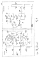
Der bekannte Komplementärverstärker von Fig. 1 enthält in Reihenschaltung einen npn-Transistor Q1 und einen pnp-Transistor Q2 zwischen zwei Spannungsanschlüssen +Ub und -Ub, die von zwei in Reihe geschalteten Spannungsquellen V2, V3 gespeist sind. Der Verbindungsknoten dieser Spannungsquellen ist mit dem Massepotential GND verbunden und mit einem Anschluss der Last RL. Der andere Anschluss dieser Last RL liegt am Verbindungsknoten der beiden Transistoren Q1, Q2. Für die Ruhestromeinstellung der beiden Transistoren Q1, Q2 sorgt eine einstellbare Vorspannungsquelle Vbias zwischen den beiden Basen dieser Transistoren. Durch geeignete Einstellung der Vorspannung Vbias lässt sich der Ruhestrom der beiden Transistoren so einstellen, dass sie z.B. jeweils im AB-Verstärkungsbetrieb arbeiten. Die unsymmetrische Eingangsspannung wird über einen Eingang +in der Basis des npn-Transistors zugeführt. Der Komplementärverstärker ist bezüglich des masseabgewandten Lastanschlusses nichtinvertierend. Kondensatoren zur Potentialtrennung sind in Fig. 1 nicht dargestellt. Sie sind jedenfalls dann erforderlich, wenn dem Eingangssignal eine Gleichspannung überlagert ist und der Eingangsspannungshub nicht sehr groß gegenüber der Basis-Emitterspannung von Transistor Q1 ist.The known complementary amplifier of Fig. 1 includes in series an NPN transistor Q1 and a pnp transistor Q2 between two voltage terminals + Ub and -Ub, which are fed by two series-connected voltage sources V2, V3. The connection node of these voltage sources is at the ground potential GND connected and connected to a terminal of the load RL. The other connection of this load RL is located at the connection node of the two transistors Q1, Q2. For the Closed-circuit current setting of the two transistors Q1, Q2 provides an adjustable Bias source Vbias between the two bases of these transistors. By suitable adjustment of the bias voltage Vbias can be the quiescent current of the two Set transistors to be e.g. each working in AB amplification mode. The unbalanced input voltage is via an input + in the base of the npn transistor fed. The complementary amplifier is remote with respect to the mass Non-inverting load connection. Capacitors for potential separation are shown in FIG. 1 not shown. In any case, they are necessary if the input signal has a DC voltage is superimposed and the input voltage swing is not very large to the base-emitter voltage of transistor Q1.
Der bekannte Komplementärverstärker nach Fig. 2 erfordert im Unterschied zu Fig. 1 nur eine Spannungsquelle V4 für die beiden in Reihe geschalteten Komplementärtransistoren Q3, Q4 aus einem npn- und einem pnp-Transistor, die zwischen einem positiven Versorgungsanschluss +Ub und dem Masseanschluss GND liegen. Die Spannungsquelle V4 liegt mit ihrem einen Anschluß an Masse GND und speist mit dem anderen den Versorgungsanschluss +Ub. Die Ruhestromeinstellung für die beiden Transistoren erfolgt wie in Fig. 1 über eine einstellbare Vorspannungsquelle Vbias, die zwischen den beiden Basisanschlüssen liegt. Da der gemeinsame Emitteranschluss bei dieser Komplementärschaltung auch näherungsweise nicht mehr auf dem Massepotential GND liegt, gibt es im Ruhezustand eine Spannungsdifferenz zwischen dem gemeinsamen Emitteranschluss und der Masse GND, die etwa der halben Versorgungsspannung V4 entspricht. Die zwischen diesen beiden Knoten anzuschließende Last RL muss, falls sie einen Gleichstrompfad aufweist, daher von dieser Gleichspannung durch einen Koppelkondensator C2 getrennt werden. Zusätzlich zu diesem Koppelkondensator C2 muss der Signaleingang +in ebenfalls durch einen Kondensator spannungsmäßig von der Signalquelle getrennt werden, da der Signaleingang +in etwa ebenfalls die halbe Versorgungsspannung V4 aufweist und damit in der Regel sich sehr vom Ruhepotential der Signalquelle unterscheidet.The known complementary amplifier according to Fig. 2 requires in contrast to Fig. 1 only a voltage source V4 for the two series-connected complementary transistors Q3, Q4 of an npn and a pnp transistor between a positive Supply terminal + Ub and the ground terminal GND lie. The voltage source V4 is GND with its one connection to ground and feeds the other one Supply connection + Ub. The quiescent current setting for the two transistors takes place as in Fig. 1 via an adjustable bias source Vbias, between the two Basic connections is. Since the common emitter terminal in this complementary circuit Also approximately no longer lies on the ground potential GND, there is in the Idle state a voltage difference between the common emitter terminal and the ground GND, which corresponds to about half the supply voltage V4. The must be connected between these two nodes load RL, if they have a Direct current path, therefore, from this DC voltage through a coupling capacitor C2 are separated. In addition to this coupling capacitor C2, the Signal input + in also by a capacitor voltage from the Signal source are disconnected, since the signal input + in about half Supply voltage V4 and thus usually very much from the rest potential the signal source is different.
Fig. 3 zeigt den im bereits erwähnten US-Patent US 4,229,706 beschriebenen Audiogegentaktverstärker mit symmetrischem Aufbau, der in den beiden Signalpfaden DC-gekoppelt ist und dessen beide npn-Endstufentransistoren Q1, Q2 jeweils von einer schwimmenden Spannungsversorgung V1, V2 gespeist sind. Die galvanische Trennung von dem Massebezugspotential GND wird bei der schwimmenden Spannungsversorgung in der Regel mittels eines eigenen Netztransformators und einer Brückengleichrichterschaltung erreicht. Die Last RL ist zwischen den beiden Emittern angeschlossen, die auch die Fußpunkte für die über Kreuz angeschlossenen schwimmenden Versorgungsspannungen V1, V2 bilden. Das symmetrische Eingangssignal wird über die Eingänge +in und -in zugeführt, wobei der positive Eingang +in mit dem nichtinvertierenden Eingang eines in Bipolartechnik ausgeführten Operationsverstärkers U1 verbunden ist. Der negative Eingang -in ist mit dem nichtinvertierenden Eingang eines zum ersten Operationsverstärker U1 identischen zweiten Operationsverstärker U2 verbunden. Der Ausgang des ersten bzw. zweiten Operationsverstärkers ist direkt, also ohne Koppelkondensator, mit der Basis des ersten bzw. zweiten Ausgangstransistors Q1, Q2 verbunden. Die Spannungsversorgung der beiden Operationsverstärker erfolgt über zwei in Reihe geschaltete Spannungsquellen V3, V4, deren Verknüpfungspunkt an das Massepotential GND angeschlossen ist und deren masseabgewandte Pole die positive und negative Versorgungsspannung +V, -V für die beiden Operationsverstärker U1, U2 bilden.Fig. 3 shows that described in the already mentioned U.S. Patent US 4,229,706 Audio balanced amplifiers with symmetrical construction, which are in the two signal paths DC-coupled and whose two NPN output stage transistors Q1, Q2 each of a floating power supply V1, V2 are powered. The galvanic isolation from the ground reference potential GND is at the floating power supply usually by means of its own power transformer and a bridge rectifier circuit reached. The load RL is connected between the two emitters, the also the base points for the cross-connected floating supply voltages V1, V2 form. The balanced input signal is sent through the inputs + in and -in, the positive input being + in with the noninverting input connected in bipolar operating amplifier U1 is connected. Of the negative input -in is with the non-inverting input one to the first Operational amplifier U1 identical second operational amplifier U2 connected. Of the Output of the first or second operational amplifier is direct, ie without coupling capacitor, is connected to the base of the first and second output transistors Q1, Q2, respectively. The power supply of the two operational amplifiers via two in Series connected voltage sources V3, V4, whose point of connection to the ground potential GND is connected and whose mass-remote poles the positive and negative supply voltage + V, -V for the two operational amplifiers U1, U2 form.
Die Ruhestromeinstellung der beiden Ausgangstransistoren Q1, Q2 erfolgt über jeweils einen Widerstand R4 bzw. R5 zwischen dem Emitter und der negativen Versorgungsspannung -V. Den zugehörigen Basisstrom liefert der Ausgang des zugehörigen Operationsverstärkers U1 bzw. U2. Hier zeigt sich nun ein Problem, denn der durch den Widerstand R4 bzw. R5 bestimmte Strom muss identisch mit dem vom Operationsverstärker U1 bzw. U2 gelieferten Basisstrom sein, da dieser Strom nur mit den Spannungsquellen V3, V4 verknüpft ist und kein anderen Strompfad zur Verfügung steht. Es wird also nicht der Emitterruhestrom geregelt, sondern der Basisstrom. Der resultierende Emitterruhestrom, der im wesentlichen von der schwebenden Spannungsversorgung V1 bzw. V2 gespeist wird und über die Last RL zurückfließt, ist direkt vom Stromverstärkungsfaktor des jeweiligen Ausgangstransistors Q1 bzw. Q2 abhängig und streut damit, was eigentlich unerwünscht ist. Die Stromregelung, genau genommen die Regelung des Basisstromes, erfolgt durch Abgriff des jeweiligen Emitterpotentials und Rückführung über einen relativ hochohmigen Widerstand R2 bzw. R3 auf den invertierenden Eingang des ersten bzw. zweiten Operationsverstärkers U1, U2. Damit beide Emitter, die ja auch die Anschlusspunkte für die Last RL bilden, möglichst auf gleichem Potential liegen, sind diese beiden Schaltungsknoten ebenfalls über einen relativ hochohmigen Widerstand R6 miteinander verbunden und somit wird auch die Differenz der beiden Potentiale als eine Art Offsetspannung auf die invertierenden Eingänge der Operationsverstärker U1, U2 zurückgeführt. Damit im Ansteuerungsfall der relativ kleine Ruhestrom nicht die Aussteuerung der Ausgangstransistoren Q1, Q2 behindert, vergrößert sich der jeweilige Emitterstrom durch eine Widerstands-Diodenstrecke R7, D1 bzw. R8, D2, die dem jeweiligen Emitter einen niederohmigeren Strompfad nach Masse GND zur Verfügung stellt, wenn die Diode leitend wird. Es wird noch erwähnt, das durch die in Fig. 3 dargestellte Basisstromrückführung in die Operationsverstärker U1, U2 nur stromgesteuerte Endstufen, also Bipolartransistoren, angesteuert werden können, nicht jedoch spannungsgesteuerte Bauelemente.The quiescent current adjustment of the two output transistors Q1, Q2 takes place via in each case a resistor R4 or R5 between the emitter and the negative Supply voltage -V. The corresponding base current supplies the output of the associated operational amplifier U1 or U2. Here is a problem, because the current determined by the resistor R4 or R5 must be identical to that of the Operational amplifier U1 or U2 supplied base current, since this current only with the voltage sources V3, V4 is linked and no other current path available stands. So it is not regulated the emitter quiescent current, but the base current. Of the resulting emitter rest current, which is essentially from the floating Voltage supply V1 and V2 is fed and flows back across the load RL is directly from the current amplification factor of the respective output transistor Q1 or Q2 dependent and scatters with what is actually undesirable. The current regulation, exactly taken the regulation of the base current, takes place by tap of the respective Emitter potential and feedback via a relatively high resistance R2 and R3 to the inverting input of the first and second operational amplifier U1, U2. So that both emitters, which also form the connection points for the load RL, if possible at the same potential, these two circuit nodes are also connected via a relatively high resistance R6 and thus becomes also the difference of the two potentials as a kind of offset voltage on the inverting inputs of the operational amplifier U1, U2 returned. So in the Actuation case, the relatively small quiescent current is not the modulation of the Output transistors Q1, Q2 obstructed, increases the respective emitter current through a resistor diode path R7, D1 and R8, D2, the respective emitter a lower resistance current path to GND ground provides when the diode becomes conductive. It is mentioned, that by the in Fig. 3 shown Base current feedback in the operational amplifiers U1, U2 only current-controlled Power amplifiers, so bipolar transistors, can be controlled, but not voltage controlled components.
Fig. 4 zeigt schematisch das Schaltbild eines ersten Ausführungsbeispiels eines symmetrischen Gegentaktverstärkers nach der Erfindung. Die beiden Signalpfade sind symmetrisch aufgebaut und enthalten jeweils einen Vorverstärkerblock N1B bzw. N2B und einen Endverstärker M1 bzw. M2. Die Endverstärker M1, M2 sind jeweils an eine schwimmende Spannungsversorgung V1, V2 angeschlossen, wobei die Laststromkreise über eine Last RL, die zwischen den Fußpunkten der beiden Endverstärker M1, M2 angeschlossen ist, überkreuz geschlossen sind. Die beiden Fußpunkte der Endverstärker stellen auch gleichzeitig die Anschlusspunkte oder Anschlussklemmen RL1, RL2 für die extern anzuschließende Last RL dar und bilden den Signalausgang.Fig. 4 shows schematically the circuit diagram of a first embodiment of a balanced push-pull amplifier according to the invention. The two signal paths are symmetrically constructed and each contain a preamplifier block N1B and N2B and a power amplifier M1 and M2, respectively. The power amplifiers M1, M2 are each connected to one floating power supply V1, V2 connected, with the load circuits via a load RL, which is between the bases of the two power amplifiers M1, M2 is connected, are crossed over. The two bases of the power amplifier At the same time set the connection points or terminals RL1, RL2 for the externally connected load RL and form the signal output.
Die Spannungsversorgungseinrichtung der Vorverstärkerblöcke N1B, N2B enthält
mindestens zwei in Serie geschaltete Spannungsquellen V3, V4, deren Verbindungspunkt
an Masse GND liegt. Die resultierenden Versorgungsspannungen +Ub und -Ub speisen
die Versorgungsanschlüsse der Vorverstärkerblöcke, die im Ausführungsbeispiel von Fig.
4 jeweils aus einem eingangsseitigen Verstärker N1, N2 mit hoher Leerlaufverstärkung
bestehen. Der positive Pol der Ausgangsstufe der Verstärker N1, N2 ist mit der positiven
Versorgungsspannung +Ub oder mit einer anderen positiven und ebenfalls
massebezogenen Spannungsquelle gespeist. Der negative Pol der Ausgangsstufe der
Verstärker N1, N2 ist über einen Potentialdifferenzerzeuger 4, 5 mit dem zugehörigen
Lastanschluss RL1, RL2 verbunden. Über diesen Potentialdifferenzerzeuger 4, 5 fließt
ein eingeprägter Strom. Durch die hohe Leerlaufverstärkung in Verbindung mit einem
hochohmigen nichtinvertierenden und hochohmigen invertierenden Eingang, mit
vernachlässigbarer Offsetspannung und vernachlässigbarem Offsetstrom und mit einem
niederohmigen Ausgang haben die Verstärker N1, N2 ein Verhalten wie ein mehr oder
weniger idealer Operationsverstärker.The power supply of the preamplifier blocks N1B, N2B contains
at least two series-connected voltage sources V3, V4, their connection point
to ground GND is. The resulting supply voltages + Ub and -Ub feed
the supply terminals of the preamplifier blocks, which in the embodiment of FIG.
4 each from an input side amplifier N1, N2 with high open-loop gain
consist. The positive pole of the output stage of the amplifiers N1, N2 is positive
Supply voltage + Ub or with another positive and also
supplied ground-based voltage source. The negative pole of the output stage of the
Amplifier N1, N2 is connected via a
Als Endverstärker M1, M2 sind in Fig. 4 zwei Dreipole dargestellt, deren jeweilige Eingangselektrode an den Ausgang des vorausgehenden Verstärkers N1, N2 angeschlossen ist. Der erste Endverstärker M1 ist von einer schwimmenden ersten Spannungsquelle V1 und der zweite Endverstärker M2 ist von einer schwimmenden zweiten Spannungsquelle V2 gespeist. Der erste Endverstärker M1 ist über seinen ersten Versorgungsanschluss mit einem Pol der ersten Spannungsquelle V1 und über seinen zweiten Versorgungsanschluss, der auch als Endverstärkerausgang dient, mit dem ersten Ausgang RL1 und über die Last RL mit dem anderen Pol der ersten Spannungsquelle V1 verbunden. Der zweite Endverstärker M2 ist über seinen ersten Versorgungsanschluss mit einem Pol der zweiten Spannungsquelle V2 und über seinen zweiten Versorgungsanschluss, der auch als Endverstärkerausgang dient, mit dem zweiten Ausgang RL2 und über die Last RL mit dem anderen Pol der zweiten Spannungsquelle V2 verbunden,As a power amplifier M1, M2 two three-pole are shown in Fig. 4, the respective Input electrode to the output of the preceding amplifier N1, N2 connected. The first power amplifier M1 is of a floating first Voltage source V1 and the second power amplifier M2 is a floating second voltage source V2 fed. The first power amplifier M1 is over its first supply terminal with a pole of the first voltage source V1 and over its second supply terminal, which also serves as a power amplifier output, with the first output RL1 and the load RL with the other pole of the first Voltage source V1 connected. The second power amplifier M2 is over its first Supply terminal with a pole of the second voltage source V2 and via its second supply terminal, which also serves as a power amplifier output, with the second output RL2 and via the load RL to the other pole of the second Voltage source V2 connected,
Die erforderliche arbeitspunktbestimmende Steuerspannung wird in den zugehörigen
Potentialdifferenzerzeugern 4, 5 durch einen von einer Ruhestromeinstelleinrichtung Ix
mit einer einstellbaren Stromquelle I1 vorgegebenen Strom bestimmt, der über die
Potentialdifferenzerzeuger 4, 5 den gewünschten Potentialversatz erzeugt. Die mit dem
negativen Versorgungsanschluss -Ub verbundene Ruhestromeinstelleinrichtung Ix
enthält eine einstellbare Stromquelle I1, deren Strom mittels der beiden mit den
Ausgangsanschlüssen RL1, RL2 verbundenen Widerstände R2, R3 hälftig auf die beiden
Potentialdifferenzerzeuger 4, 5 aufgeteilt wird, so dass die Arbeitspunkteinstellung für die
beiden Endverstärker M1, M2 symmetrisch erfolgt.The required operating point-determining control voltage is in the associated
Dieser Einstellvorgang kann selbstverständlich auf verschiedene Weisen erfolgen, beispielsweise rein manuell wie im Ausführungsbeispiel von Fig. 4 über eine einstellbare Stromquelle I1, eine einstellbare Spannungsquelle Vbias (siehe Fig. 8) oder über ein Potentiometer, das die Stromquelle I1 steuert. Zweckmäßig ist auch eine temperaturbeeinflusste Steuerung, die über einen Temperaturfühler, der die Temperatur mindestens eines Leistungsbauelementes erfasst, die einstellbare Strom- oder Spannungsquelle I1 bzw. Vbias so beeinflusst, dass der Ruhestrom der Leistungsbauelemente der Endverstärker M1, M2 konstant bleibt oder einen vorgegebenen Temperaturverlauf aufweist. Noch weitergehend ist eine vollständige automatische Regelung dergestalt, dass der aktuelle Ruhestromwert der Leistungsbauelemente der Endverstärker M1, M2 gemessen und mit einem vorgegebenen Sollwert verglichen wird und auftretende Abweichungen vom Sollwert durch automatisches Nachstellen der Ruhestromeinstelleinrichtung Ix weggeregelt werden. Selbstverständlich sind auch Kombinationen dieser beschriebenen Regelungsmaßnahmen unter Schutz gestellt.Of course, this adjustment process can be done in different ways, For example, purely manually as in the embodiment of Fig. 4 via an adjustable Current source I1, an adjustable voltage source Vbias (see Fig. 8) or via a Potentiometer that controls the current source I1. It is also useful temperature-sensitive control, which has a temperature sensor that determines the temperature detected at least one power component, the adjustable current or Voltage source I1 or Vbias influenced so that the quiescent current of Power components of the power amplifier M1, M2 remains constant or one having predetermined temperature profile. Going further is a complete one automatic regulation such that the current quiescent current value of Power components of the power amplifiers M1, M2 measured and with a predetermined setpoint is compared and occurring deviations from the setpoint adjusted by automatic adjustment of the quiescent current setting Ix become. Of course, combinations of these are described Regulatory measures under protection.
Die beiden Verstärker N1 und N2 haben einen invertierenden und einen nichtinvertierenden
Eingang und entsprechen wegen ihrer hohen Leerlaufverstärkung jeweils einem
Operationsverstärker. Als Ausgang des resultierenden Operationsverstärkers sieht man
dabei am zweckmäßigsten den Lastanschluss RL1 bzw. RL2 an, der durch ein
Rückkopplungsnetzwerk auf das Massepotential GND geregelt wird. Das
Rückkopplungsnetzwerk wird durch die seriengeschaltete Widerstände R6 und R7 bzw.
R8 und R9 gebildet, die zwischen dem Lastanschluss RL1 und Masse GND bzw. dem
Lastanschluss RL2 und Masse GND liegen. Der gemeinsame Verbindungspunkt der
Widerstände R6, R7 bzw. R8, R9 ist mit dem invertierenden Eingang des Verstärkers N1
bzw. N2 verbunden. Der nichtinvertierende Eingang des ersten Verstärkers N1 ist mit
dem positiven Signaleingang +in und der nichtinvertierende Eingang des zweiten
Verstärkers N2 ist mit dem negativen Signaleingang -in des Gegentaktverstärkers
verbunden. Durch das Rückkopplungsnetzwerk R6, R7 bzw. R8, R9 wird der Ausgang
des Verstärkers N1 bzw. N2 so geregelt, dass über den Potentialdifferenzerzeuger 4, 5
und den Spannungsteiler R6, R7 bzw. R8, R9 das Potential am nichtinvertierenden
Eingang des Verstärkers N1 bzw. N2 identisch zum Potential am positiven bzw. negativen
Signaleingang +in bzw. -in ist. Diese Regelung über das Rückkopplungsnetzwerk ist
unabhängig von der Größe der Ruhestromeinstellung für die Leistungsbauelemente der
Endverstärker M1, M2, die durch die einstellbare Stromquelle I1 vorgegeben ist. Der
resultierende Pegelversatz am Potentialdifferenzerzeuger 4 bzw. 5 wird durch den
Verstärker N1 bzw. N2 ausgeregelt.The two amplifiers N1 and N2 have one inverting and one non-inverting one
Input and correspond due to their high idle gain each one
Operational amplifier. As an output of the resulting operational amplifier you can see
most conveniently the load connection RL1 or RL2, which by a
Feedback network is regulated to the ground potential GND. The
Feedback network is through the series-connected resistors R6 and R7 or
R8 and R9 formed between the load terminal RL1 and ground GND and the
Load connection RL2 and ground GND are. The common connection point of the
Resistors R6, R7 and R8, R9 is connected to the inverting input of the amplifier N1
or N2 connected. The non-inverting input of the first amplifier N1 is with
the positive signal input + in and the non-inverting input of the second
Amplifier N2 is connected to the negative signal input -in the push-pull amplifier
connected. Through the feedback network R6, R7 and R8, R9 is the output
of the amplifier N1 or N2 regulated so that via the
Die Widerstände R10 und R11 vom positiven bzw. negativen Signaleingang nach Masse GND haben für die Rückkopplung keine Bedeutung. Sie dienen lediglich der Festlegung des GND-Potentiales für die jeweiligen nichtinvertierenden Eingänge von N1 und N2 sowie der Leitungsanpassung, da die Signaleingänge an den nichtinvertierenden Eingängen der Verstärker N1 und N2 in der Regel hochohmig sind. Später wird ein Ausführungsbeispiel gezeigt, bei dem die Signaleingänge an die invertierenden Eingänge der Verstärker N1 und N2 angeschlossen sind. Durch das an diese Eingänge angeschlossene Rückkopplungsnetzwerk sind diese Eingänge dann wesentlich niederohmiger, so das eine Leitungsanpassung gegebenenfalls entfallen kann. The resistors R10 and R11 from the positive and negative signal input to ground GND have no meaning for the feedback. They are only for determination the GND potential for the respective noninverting inputs of N1 and N2 and the line adaptation, since the signal inputs to the noninverting Inputs of amplifiers N1 and N2 are usually high impedance. Later will be one Embodiment shown in which the signal inputs to the inverting inputs the amplifiers N1 and N2 are connected. By the to these inputs connected feedback network, these inputs are then essential low impedance, so that a line adjustment may be omitted if necessary.
Um einen erfindungsgemäß vollsymmetrischen Verstärker für ein symmetrisches Eingangssignal zu realisieren, müssen die entsprechenden Widerstände in den beiden Signalzweigen selbstverständlich gleich sein. Es gilt R6 = R8 und R7 = R9. Das Verhältnis der Widerstände R6/R7 bzw. R8/R9 bestimmt die Gesamtverstärkung des Gegentaktverstärkers.To a fully symmetrical according to the invention amplifier for a symmetric To realize input signal, the corresponding resistors must be in the two Of course, signal branches will be the same. R6 = R8 and R7 = R9. The Ratio of resistors R6 / R7 or R8 / R9 determines the overall gain of Push-pull amplifier.
Die obere Verstärkerhälfte, im wesentlichen aus den Baugruppen N1B und M1 bestehend, verstärkt die eine Halbwelle des symmetrischen Eingangssignals und die untere Verstärkerhälfte, bestehend aus den Baugruppen N2B und M2, verstärkt die andere Halbwelle.The upper amplifier half, essentially of the modules N1B and M1 consisting amplifies the one half-wave of the balanced input signal and the lower amplifier half, consisting of the modules N2B and M2, amplifies the another half wave.
Die Endverstärker M1, M2 können auf vielfältige Weise praktisch realisiert werden: als einzelne Leistungsbauelemente wie z.B. Leistungs-MOSFETs, IGBTs oder bipolare Leistungstransistoren, aber auch vorteilhaft aus Kombinationen gleichartiger oder verschiedener Verstärkerbauelemente mit oder ohne lokale Gegenkopplung.The power amplifiers M1, M2 can be practically implemented in a variety of ways: as individual power devices such as e.g. Power MOSFETs, IGBTs or bipolar Power transistors, but also advantageous combinations of the same or various amplifier components with or without local negative feedback.
Im Schaltbild von Fig. 5 ist die Ausgangsstufe der Vorverstärkerblöcke N1B und N2B
beispielhaft als Triode Xtr1 bzw. Xtr2 ausgeführt. Im Ausführungsbeispiel von Fig. 5
bestehen die Vorverstärkerblöcke N1B und N2B damit jeweils aus der Kombination eines
eingangsseitigen Verstärkers N1, N2 mit hoher Leerlaufverstärkung und einer an den
Verstärker N1, N2 angeschlossenen Röhre Xtr1, Xtr2, deren Steuergitter mit dem
zugehörigen Verstärkerausgang verbunden ist. Die Anode der Röhre Xtr1, Xtr2 ist mit der
positiven Versorgungsspannung +Ub oder mit einer anderen positiven und ebenfalls
massebezogenen Spannungsquelle verbunden. Die Kathode der Röhre Xtr1, Xtr2 ist über
einen Potentialdifferenzerzeuger 4, 5, der im einfachsten Fall einen Widerstand R4, R5
enthält und über den ein eingeprägter Strom fließt, mit dem zugehörigen Lastanschluss
RL1, RL2 verbunden.In the circuit diagram of Fig. 5, the output stage of the preamplifier blocks N1B and N2B
exemplified as triode Xtr1 or Xtr2 executed. In the embodiment of FIG. 5
Thus, the preamplifier blocks N1B and N2B each consist of the combination of a
input side amplifier N1, N2 with high open-loop gain and one to the
Amplifier N1, N2 connected tube Xtr1, Xtr2, whose control grid with the
associated amplifier output is connected. The anode of the tube Xtr1, Xtr2 is with the
positive supply voltage + Ub or with another positive and also
mass-related voltage source connected. The cathode of the tube Xtr1, Xtr2 is over
a
Für die im Ausführungsbeispiel Fig. 5 als Trioden dargestellten Röhren Xtr1, Xtr2 können selbstverständlich auch Tetroden, Pentoden, Hexoden und Heptoden mit dem Stand der Technik entsprechender Beschaltung der zusätzlichen Gitter eingesetzt werden.For the tubes Xtr1, Xtr2 shown as triodes in the embodiment of FIG Of course, tetrodes, pentodes, hexodes and heptodes with the state of Technology corresponding wiring of the additional grid can be used.
Als Endverstärker M1, M2 sind in Fig. 5 zwei n-Kanal-MOSFETs dargestellt, deren
jeweilige Gateelektrode an die Kathode der vorausgehenden Röhre Xtr1, Xtr2
angeschlossen ist. Die jeweilige Sourceelektrode ist mit dem zugehörigen Lastanschluss
RL1, RL2 und die jeweilige Drainelektrode mit dem positiven Potential der
schwimmenden Spannungsquelle V1, V2 verbunden. Die arbeitspunktbestimmende Gate-Source-Steuerspannung
wird in den zugehörigen Potentialdifferenzerzeugern 4, 5 durch
einen von einer Ruhestromeinstelleinrichtung Ix mit einer einstellbaren Stromquelle I1
vorgegebenen Strom bestimmt, der über die Widerstände R4, R5 den gewünschten
Potentialversatz erzeugt. Die mit dem negativen Versorgungsanschluss -Ub verbundene
Ruhestromeinstelleinrichtung Ix enthält eine einstellbare Stromquelle I1, deren Strom
mittels der beiden mit den Ausgangsanschlüssen RL1, RL2 verbundenen Widerstände
R2, R3 hälftig auf die beiden Widerstände R4, R5 aufgeteilt wird, so dass die
Arbeitspunkteinstellung für die beiden MOSFETs M1, M2 symmetrisch erfolgt.As power amplifier M1, M2, two n-channel MOSFETs are shown in Fig. 5, whose
respective gate electrode to the cathode of the preceding tube Xtr1, Xtr2
connected. The respective source electrode is connected to the associated load connection
RL1, RL2 and the respective drain electrode with the positive potential of
floating voltage source V1, V2 connected. The operating point-determining gate-source control voltage
is in the associated
Zur Vereinfachung der Funktionsbeschreibung wurde entsprechend dem Ausführungsbeispiel
von Fig. 4 zunächst davon ausgegangen, dass die Verstärker N1 und N2 ein
Verhalten wie ein idealer Operationsverstärker haben. Die Ausführungsbeispiele ab Fig. 5
gehen davon aus, dass die aktiven Bauelemente in den beiden Signalzweigen von den
idealen Eigenschaften abweichen und auch bezüglich der Symmetriebedingung mehr
oder weniger zueinander unterschiedlich sind. Mittels ergänzender Regelkreise nach
Weiterbildungen der Erfindung lassen sich aber derartige Unzulänglichkeiten für die
Gesamtfunktion des Gegentaktverstärkers beseitigen.To simplify the functional description was according to the
Im Schaltbild von Fig. 5 ist schematisch eine derartige Regelungsanordnung als "Biasregelung" B1 dargestellt, die den Gegentaktverstärker von Fig. 4 ergänzt. Da gleiche Schaltungs- und Funktionseinheiten in allen Figuren der Zeichnung mit gleichen Bezugszeichen versehen sind, erübrigen sich wiederholende Funktionsbeschreibungen. Der Schaltungsblock B1 enthält zwei Regelkreise B2, B3, deren Eingänge mit den Verstärkerausgängen RL1, RL2 und deren Ausgänge mit den Rückführungsnetzwerken der beiden Vorverstärkerblöcke N1B bzw. N2B verkoppelt sind.In the diagram of Fig. 5 is schematically such a control arrangement as "Biasregelung" B1, which complements the push-pull amplifier of Fig. 4. Same thing Circuit and functional units in all figures of the drawing with the same Reference signs are provided, unnecessary repetitive descriptions of functions. The circuit block B1 contains two control circuits B2, B3 whose inputs are connected to the Amplifier outputs RL1, RL2 and their outputs with the feedback networks the two preamplifier blocks N1B and N2B are coupled.
Der Eingang des ersten Regelkreises B2 wird durch zwei in Serie geschaltete gleichgroße
Widerstände R16, R17 gebildet, die an die Ausgänge RL1, RL2 angeschlossen sind und
deren gemeinsamer Verbindungspunkt avg über einen Widerstand R15 auf den
invertierenden Eingang eines Operationsverstärkers U3 geschaltet ist. Am
nichtinvertierenden Eingang von U3 ist eine Gleichspannung V5 angelegt. Der Ausgang
des Verstärkers U3 ist mittels eines Kondensators C2 auf den nichtinvertierenden
Eingang zurückgeführt. Die Spannungsversorgung des Verstärkers U3 erfolgt
zweckmäßigerweise über die bereits vorhandenen Versorgungspotentiale +Ub und -Ub
oder über eine andere Versorgungsspannung. Ein am Ausgang von U3 angeschlossener
Inverter N3 invertiert das Ausgangsignal und führt es über einen Widerstand R18 auf den
gemeinsamen Verbindungspunkt der Widerstände R8, R9 und damit invertierenden
Eingang des Verstärkers N2 zurück. Für die weitere Betrachtung wird dieser
Schaltungsknoten, der eine wichtige Schnittstelle für die Regelung und in Fig. 5 auch als
Leitung dargestellt ist, mit "bias 1" bezeichnet. Eine zweite Rückführung des
Ausgangssignals von Verstärker U3 erfolgt über einen Widerstand R19 auf den
gemeinsamen Verbindungspunkt der Widerstände R6, R7 und damit invertierenden
Eingang des Verstärkers N1. Für die weitere Betrachtung wird dieser Schaltungsknoten,
der ebenfalls eine wichtige Schnittstelle für die Regelung und in Fig. 5 auch als Leitung
dargestellt ist, mit "bias 2" bezeichnet.The input of the first control circuit B2 is equal by two connected in series
Resistors R16, R17 are formed, which are connected to the outputs RL1, RL2 and
their common connection point avg via a resistor R15 on the
inverting input of an operational amplifier U3 is connected. At the
non-inverting input of U3, a DC voltage V5 is applied. The exit
of the amplifier U3 is by means of a capacitor C2 to the non-inverting
Entrance returned. The power supply of the amplifier U3 takes place
expediently via the already existing supply potentials + Ub and -Ub
or via another supply voltage. One connected to the output of U3
Inverter N3 inverts the output signal and leads it via a resistor R18 to the
common connection point of the resistors R8, R9 and thus inverting
Input of amplifier N2 back. For further consideration, this is
Circuit node, which is an important interface for the control and in Fig. 5 also as
Line is shown, labeled "
Der Eingang des zweiten Regelkreises B3 wird durch einen Subtrahierer D1 gebildet,
dessen Minuendeingang + mit dem Lastanschluss RL2 und dessen Subtrahendeingang -
mit dem Lastanschluss RL1 verbunden ist. Der Ausgang des Subtrahierers D1 bestimmt
das Potential des Knotens diff und ist über einen Widerstand R14 mit dem invertierenden
Eingang eines Verstärkers U4 verbunden, der über einen Kondensator C1 mit seinem
Verstärkerausgang verbunden ist. Dieser Ausgang ist ferner über eine Serienschaltung
aus einem Inverter N4 und einem Widerstand R12 mit dem Schaltungsknoten bias 1 und
über einen Widerstand R13 mit dem anderen Schaltungsknoten bias 2 verbunden. Am
nichtinvertierenden Eingang des Verstärkers U4 ist das Massepotential GND
angeschlossen.The input of the second control loop B3 is formed by a subtractor D1,
whose Minuendeingang + with the load terminal RL2 and its Subtrahendeingang -
is connected to the load terminal RL1. The output of the subtracter D1 determines
the potential of the node is diff and is connected to the inverting resistor R14
Input of an amplifier U4 connected via a capacitor C1 with his
Amplifier output is connected. This output is also via a series circuit
from an inverter N4 and a resistor R12 to the
Die erfindungsgemäße Funktion des Regelungsblockes Biasregelung B1 besteht darin, dass mittels der ersten Regelungsschleife B2 der Mittelwert avg der Potentiale an den Ausgängen RL1, RL2 erfasst und mit einer vorgegebenen Sollspannung V5 verglichen wird. Über den vom Verstärker U3 gebildeten Integrator wird die Abweichung des Potentials avg vom Sollwert V5 verstärkt. Mittels des Invertierers N3 und der Widerstände R18 und R19 wirkt diese verstärkte Abweichung vom Sollwert V5 in gleicher Weise so auf die beiden direkt gekoppelten Regelschnittstellen bias 1 und bias 2 ein, dass der Mittelwert der Potentiale an den Ausgangsanschlüssen RL1, RL2 auf den vorgegebenen Sollwert V5 eingeregelt wird. Damit wird der Betrag des Absolutpotentials der Ausgänge RL1, RL2 definiert eingestellt.The function of the control block bias control B1 according to the invention is to that by means of the first control loop B2, the mean value avg of the potentials at the Outputs RL1, RL2 detected and compared with a predetermined target voltage V5 becomes. About the integrator formed by the amplifier U3 is the deviation of Potential avg amplified from the setpoint V5. By means of the inverter N3 and the resistors R18 and R19 act in the same way on this increased deviation from the setpoint V5 the two directly coupled rule interfaces bias 1 and bias 2 indicate that the Average of the potentials at the output terminals RL1, RL2 to the predetermined Setpoint V5 is adjusted. This will be the magnitude of the absolute potential of the outputs RL1, RL2 defined set.
Mittels der zweiten Regelungsschleife B3 wird der zeitliche Mittelwert der vorzeichenbehafteten
Differenz diff der Potentiale an den Ausgängen RL1, RL2 erfasst, dieser Wert
mit einer vorgegebenen Sollspannung verglichen und Abweichungen mittels des aus dem
Verstärker U4 gebildeten Integrators über die beiden Regelschnittstellen bias 1 und bias
2 ausgeregelt. Da die Differenzspannung in der Regel vernachlässigbar klein sein soll,
also im Bereich von 0 V, wird dem Referenzeingang (=nichtinvertierenden Eingang) des
Verstärkers U4 als Referenzspannung das Massepotential GND zugeführt. Da mögliche
Abweichungen sich in der Regelrichtung unterschiedlich auf die beiden Regelschnittstellen
bias 1, bias 2 auswirken müssen, ist in die Rückführung auf die Schnittstelle bias 1
der Inverter N4 eingefügt.By means of the second control loop B3 is the time average of the signed
Difference diff of the potentials detected at the outputs RL1, RL2, this value
compared with a predetermined target voltage and deviations by means of the
Amplifier U4 formed integrator via the two rule interfaces bias 1 and bias
2 adjusted. Since the differential voltage is usually negligible,
ie in the range of 0 V, the reference input (= non-inverting input) of the
Amplifier U4 supplied as reference voltage to the ground potential GND. As possible
Deviations differ in the control direction differently on the two control interfaces
bias 1, bias 2 is in the return to the
Die Zeitkonstante τ2 = R14 * C1 der zweiten Regelschleife B3 wird so gewählt, dass keine Beeinflussung der zu verstärkenden Wechselspannungssignale (=AC-Signale) im vorgesehenen Nutzfrequenzbereich des Gegentaktverstärkers erfolgt. Für den Einsatz als Audioverstärker ist beispielsweise τ2 größer oder gleich 1s sinnvoll.The time constant τ2 = R14 * C1 of the second control loop B3 is selected so that no influence on the AC signals to be amplified (= AC signals) in the provided useful frequency range of the push-pull amplifier takes place. For use as Audio amplifier, for example, τ2 greater than or equal to 1s makes sense.
Die Zeitkonstante τ1 = R15 * C2 der ersten Regelschleife B2 wird so eingestellt, dass ebenfalls ein Wert größer oder gleich 1s erreicht wird, um bei eventuellen Abweichungen vom idealen symmetrischen Verhalten eine Beeinflussung der zu verstärkenden AC-Signale im vorgesehenen Nutzfrequenzbereich zu vermeiden.The time constant τ1 = R15 * C2 of the first control loop B2 is set so that also a value greater than or equal to 1s is reached, in case of deviations from the ideal symmetric behavior influencing the AC signals to be amplified to avoid in the intended use frequency range.
Werden die Verstärker N1 bzw. N2 in den Vorverstärkerblöcken so realisiert, dass im Ruhezustand ein erheblicher, auch driftbelasteter, Potentialunterschied zwischen dem nichtinvertierenden und dem invertierendem Eingang dieser Verstärker N1, N2 auftritt, so kann durch eine geeignete Ausführung der Biasregelung dieser störende Einfluss auf die Arbeitspunktstabilität minimiert werden.If the amplifiers N1 or N2 in the preamplifier blocks realized so that in Hibernation a significant, also driftbelasteter, potential difference between the noninverting and the inverting input of these amplifiers N1, N2 occurs, so can by means of a suitable design of the bias control this disturbing influence on the Working point stability can be minimized.
Ein derartiger Fall ergibt sich beispielsweise, wenn die Verstärker N1, N2 nicht in
Halbleitertechnik sondern in Röhrentechnik ausgeführt sind. Dabei könnte zum Beispiel
die erste Stufe eines Röhrenverstärkers als Kathodenbasisstufe realisiert sein. In diesem
Fall entspricht zum Beispiel das Gitter dem nichtinvertierenden Eingang des Verstärkers
N1 bzw. N2 und die Kathode dem invertierenden Eingang von N1 bzw. N2. Durch den
Kathodenstrom ergibt sich eine Potentialanhebung über den Widerstand R7 bzw. R9.
Würde wie in dem Beispiel von Fig. 5 die Sollspannung V5 = 0V betragen, so würde
durch das dann im Ruhezustand auf 0V eingeregelte Absolutpotential von RL1 bzw. RL2
eine Potentialdifferenz über die Rückkopplungswiderstände R6 und R8 entstehen. Das
führt wiederum zu einer anteiligen Biasstromaufteilung in Abhängigkeit von den
Widerständen R2, R4, R6 bzw. R3, R5, R8 mit:
Die Arbeitspunkte von Röhren sind thermischen und alterungsbedingten Schwankungen unterworfen. Damit ändert sich über die Temperatur und die Alterung der Eingangsröhren, die im wesentlichen die Spannungsverstärkung in den Verstärkern N1 bzw. N2 bewirken, der Stromanteil I(R6) bzw. I(R8), und damit nach der ersten Beziehung das durch I(R4) bestimmte Potential der Gate-Source-Strecke des Endverstärkers M1. Entsprechend negativ wirkt sich das durch den Strom I(R5) bestimmte Potential auf die Gate-Source-Strecke des Endverstärkers M2 aus. Um diesen störenden Einfluss auszuschließen oder zumindest zu minimieren wird die Sollspannung V5 nicht fest eingestellt, sondern wie im Ausführungsbeispiel von Fig. 6 werden die Regelschnittstellen bias 1 und bias 2 über die in Reihe geschalteten gleichgroßen Widerstände R24 und R25 miteinander verknüpft, so dass an dem gemeinsamen Widerstandsabgriff eine neue Knotenspannung avgln für einen dritten Regelkreis B4 zur Verfügung steht. Diese Knotenspannung avgln wird über einen Widerstand R26 auf den nichtinvertierenden Eingang des Regelverstärkers U3 geführt, der anders als in Fig. 5 nicht mit einer Referenzspannung V5 gespeist ist, sondern der seine Referenzspannung an diesem Anschluss selbst erzeugt, indem ein Kondensator C3 dort angeschlossen ist. Der Mittelwert der Potentiale an den Regelschnittstellen bias 1 und bias 2 wird somit über das RC-Glied R26 und C3 tiefpassgefiltert und dient dann als Sollspannung am nichtinvertierenden Eingang des Regelverstärkers U3. Die Eckfrequenz des RC-Gliedes R26, C3 wird bevorzugt mindestens eine Dekade tiefer als die unterste zu übertragende Nutzsignalfrequenz gewählt. Durch diese in Fig. 6 dargestellte Schaltungsvariante wird der grundsätzliche oder driftbedingte Potentialunterschied zwischen den Eingängen der Verstärker N1 bzw. N2, auf die über das Gegenkopplungsnetzwerk ein Teil der Ausgangsspannung zurückgeführt wird, und den Ausgangsknoten RL1 bzw. RL2 ideal zu Null geregelt oder zumindest so klein, dass damit der Fehleranteil der Ruhestromregelung keinen Einfluss mehr hat.The operating points of tubes are thermal and aging-related fluctuations subjected. This changes the temperature and the aging of the input tubes, essentially the voltage gain in the amplifiers N1 and N2 cause the current component I (R6) or I (R8), and thus after the first relationship the by I (R4) certain potential of the gate-source path of the power amplifier M1. Accordingly, the potential determined by the current I (R5) has a negative effect on the Gate-source path of the power amplifier M2 off. To this disturbing influence to exclude or at least minimize the target voltage V5 is not fixed set, but as in the embodiment of Fig. 6, the rule interfaces bias 1 and bias 2 across series connected equal resistances R24 and R25 linked together, so that at the common resistor tap a new Node voltage avgln is available for a third loop B4. These Node voltage avgln is connected through a resistor R26 to the noninverting Input of the control amplifier U3 out, the unlike in Fig. 5 not with a Reference voltage V5 is fed, but its reference voltage at this Connection itself generated by a capacitor C3 is connected there. Of the Mean value of the potentials at the control interfaces bias 1 and bias 2 is thus over the RC element R26 and C3 low-pass filtered and then serves as a target voltage on non-inverting input of the control amplifier U3. The corner frequency of the RC element R26, C3 is preferably at least one decade lower than the lowest to be transferred Payload frequency selected. By this circuit variant shown in Fig. 6 is the fundamental or drift - related potential difference between the inputs of the Amplifier N1 or N2, on the negative feedback network part of the Output voltage is returned, and the output node RL1 or RL2 ideal to Zero regulated or at least so small that with it the error portion of the Closed-circuit current control has no influence.
Wie bereits erwähnt, besteht ein wesentlicher Vorteil des durch die Erfindung vorgeschlagenen Gegentakt-Verstärkerprinzips in der weitgehend freien Wahl der aktiven Bauelemente. Zum Beispiel können als Leistungsbauelemente alle bekannten Bauelementetypen verwendet werden. In den Ausführungsbeispielen von Fig. 5 und Fig. 6 wurden als Endverstärker M1, M2 exemplarisch n-Kanal-MOSFETs gezeigt. Ohne Strukturänderung können in diesen Schaltungen auch andere Leistungsbauelemente verwendet werden, auch solche die nicht selbstleitend sind wie z.B. IGBTs und Bipolartransistoren. Werden selbstleitende Bauelemente, die eine negative Vorspannung erfordern, beispielsweise Röhren und einige JFETs, eingesetzt, kann durch eine geringfügige Änderung der Schaltungsstruktur die erfindungsgemäße Funktionsweise in gleicher Weise gesichert werden. Ein hierzu gehöriges Prinzipschaltbild eines entsprechenden Ausführungsbeispieles zeigt Fig. 7.As already mentioned, there is a significant advantage of the invention proposed push-pull amplifier principle in the largely free choice of active Components. For example, as power devices all known Component types are used. In the exemplary embodiments of FIG. 5 and FIG. 6 have been shown as power amplifiers M1, M2 by way of example n-channel MOSFETs. Without Structural change may also include other power devices in these circuits be used, even those that are not self-conducting such. IGBTs and Bipolar transistors. Be self-conducting components that have a negative bias require, for example, tubes and some JFETs used, can by a slight change in the circuit structure, the inventive operation in be secured in the same way. An associated schematic diagram of a corresponding embodiment, Fig. 7.
In Fig. 7 ist ein Ausführungsbeispiel des Gegentaktverstärkers dargestellt, der als
Endverstärker M1, M2 jeweils Röhren Xtr3, Xtr4 aufweist, die direkt die Last RL treiben.
Die Vorverstärkerblöcke N1B, N2B enthalten im Gegensatz zu den vorausgehenden
Ausführungsbeispielen nach Fig. 5 und Fig. 6 keine Kombinationsverstärker, sondern
bestehen allein aus den Verstärkern N1, N2. Diese sind so realisiert, dass sie im
Ruhezustand eine negative Ausgangsgleichspannung von einigen Volt bis einigen zehn
Volt je nach den angeschlossenen Röhren Xtr3, Xtr4 aufweisen. Die einstellbare
Stromquelle I1 ist hierzu an ein positives Potential +Ub geschaltet, so dass deren hälftiger
Strom über die Widerstände R2, R3, die Pegelumsetzer 4, 5 und die interne
Ausgangsstufe von N1, N2 zur negativen Versorgungsspannung -Ub fließt. Dieser
Stromfluss verursacht an den Widerständen R4, R5 die erforderliche negative
Gittervorspannung für die Röhren Xtr3 bzw. Xtr4. Es wird damit wieder mit nur einer
Stellgröße der Ruhestrom beider Röhren Xtr3, Xtr4 in den schwimmenden ohne festen
Massebezug betriebenen Endverstärkern M1, M2 definiert und synchron sowie
symmetrisch eingestellt. Wie schon weiter oben beschrieben, kann der Einstellvorgang
von 11 und damit der Ruhestrom der Röhren Xtr3, Xtr4 auf vielfältige Weise manuell,
temperaturgesteuert oder mittels eines automatischen Ruhestromregelkreises ausgeführt
werden. In der beispielhaften Darstellung von Fig. 7 wurden Trioden verwendet. Für Xtr3,
Xtr4 können aber alle bekannten Röhrentypen wie z.B. auch Tetroden und Pentoden
eingesetzt werden.In Fig. 7, an embodiment of the push-pull amplifier is shown, as
Power amplifiers M1, M2 each have tubes Xtr3, Xtr4, which directly drive the load RL.
The preamp blocks N1B, N2B contain, unlike the previous ones
Embodiments of FIG. 5 and FIG. 6 no combination amplifier, but
consist solely of the amplifiers N1, N2. These are so realized that they are in the
Hibernate a negative DC output voltage from a few volts to a few tens
Volts depending on the connected tubes Xtr3, Xtr4 have. The adjustable
Current source I1 is connected to a positive potential + Ub, so that half their
Current through the resistors R2, R3, the
Muss die Last RL in einem speziellen Bedarfsfall mittels eines Übertragers an die mit Röhren ausgestattete Leistungsendstufe M1, M2 angekoppelt werden, kann dies mit der gleichen Struktur wie in Fig. 7 erfolgen, nur dass dann statt der direkten Lastankopplung ein Übertrager in bekannter Art und Weise den Innenwiderstand der Röhrenendstufe an die niederohmige Last heruntertransformiert. Der Übertrager kann dabei kostensparend als Spartransformator ausgeführt werden, da durch die erfindungsgemäße Ruhestromeinstellung keine Gleichstromvormagnetisierung auftritt. Zweckmäßigerweise wird der Spartransformator symmetrisch gewickelt, beispielsweise in einem Zweikammeraufbau, so dass sich gleiche Wicklungswiderstände für beide Wicklungshälften ergeben. Dank der fehlenden Gleichstromvormagnetisierung ist auch eine Realisierung als Ringkerntransformator möglich. Die Wicklung wird in diesem Fall auf ganzzahlige gleiche Teile aufgeteilt, die dann paarweise bifilar gewickelt werden. Eine Abweichung vom Symmetrieprinzip, beispielsweise durch einfaches Aufeinanderwickeln der jeweiligen Wicklungen, ermöglicht immer noch eine stabile Arbeitsweise des erfindungsgemäßen Gegentaktverstärkers, schöpft dessen Möglichkeiten aber nicht voll aus.Must the load RL in a special case by means of a transformer to the with Tubular equipped power amplifier M1, M2 can be coupled with the the same structure as in Fig. 7, except that then instead of the direct load coupling a transformer in a known manner to the internal resistance of the tube output stage the low-impedance load stepped down. The transformer can save costs be executed as autotransformer, since by the inventive Closed-circuit current setting no DC bias occurs. Conveniently, the autotransformer is wound symmetrically, for example in a two-chamber design, so that the same winding resistances result for both winding halves. Due to the lack of DC biasing is also a realization as a toroidal transformer possible. In this case, the winding will be the same as an integer Split parts, which are then wrapped in pairs bifilar. A deviation from Symmetry principle, for example, by simply winding up the respective Windings, still allows a stable operation of the invention Push-pull amplifier, but does not fully exploit its possibilities.
Ein weiteres Ausführungsbeispiel des erfindungsgemäßen Gegentaktverstärkers zeigt Fig. 8. Diese Schaltung ist nahezu identisch zur Schaltung von Fig. 6, nur dass die Stellgröße für die Ruhestromeinstellung nicht wie in Fig. 6 durch die einstellbare Stromquelle I1 erfolgt, sondern durch eine einstellbare Spannungsquelle Vbias, die letztendlich über die Widerstände R2, R3 aber ebenfalls einen Strom erzeugt, der mittels dieser Widerstände R2, R3 hälftig aufgeteilt wird und über die Widerstände R4, R5 den gewünschten arbeitspunktbestimmenden Potentialversatz für die jeweilige Gate-Source-Strecke der beiden n-Kanal-MOSFETs im Endverstärker M1, M2 erzeugt.Another embodiment of the push-pull amplifier according to the invention shows Fig. 8. This circuit is almost identical to the circuit of Fig. 6, except that the Control value for the quiescent current setting not as in Fig. 6 by the adjustable Current source I1, but by an adjustable voltage source Vbias, the Ultimately via the resistors R2, R3 but also generates a current that means these resistors R2, R3 is divided in half and the resistors R4, R5 the desired operating point determining potential offset for the respective gate-source path of the two n-channel MOSFETs in the power amplifier M1, M2 generated.
Erfindungsgemäß ist der Absolutwert der Potentiale an den Lastanschlüssen RL1, RL2 definiert und auf einen annähernd gleichen Wert eingeregelt. Da die Widerstände R2 und R3 einander gleich sind, sind auch die durch sie hindurchfließenden Ströme I(R2) und I(R3) einander gleich. Diese Ströme fließen annähernd vollständig über die Widerstände R4 bzw. R5 und von der Kathode zur Anode der Triode Xtr1 bzw. Xtr2 zur positiven Betriebsspannung +Ub. Durch den resultierenden Potentialversatz an den Widerständen R4 bzw. R5 wird ein definierter positiver Potentialunterschied zwischen der Gate-Source-Strecke der MOSFETs M1 bzw. M2 erzeugt und damit fließt folgerichtig ein definierter Ruhestrom durch diese Endstufentransistoren. Der Einstellvorgang der Spannungsquelle Vbias kann wieder auf vielfältige Weise erfolgen, manuell, temperaturgesteuert oder mittels eines automatischen Ruhestromregelkreises.According to the invention, the absolute value of the potentials at the load terminals RL1, RL2 defined and adjusted to an approximately equal value. Since the resistors R2 and R3 are equal to each other, are also the flows flowing through them I (R2) and I (R3) equal to each other. These currents flow almost completely across the resistors R4 or R5 and from the cathode to the anode of the triode Xtr1 and Xtr2 to the positive Operating voltage + Ub. Due to the resulting potential offset on the resistors R4 or R5 becomes a defined positive potential difference between the gate-source path the MOSFETs M1 and M2 generated and thus flows logically a defined Quiescent current through these output stage transistors. The adjustment process of the voltage source Vbias can again be done in a variety of ways, manually, temperature controlled or by means of an automatic quiescent current control circuit.
Entsprechend dem Ausführungsbeispiel von Fig. 9 ist ein erfindungsgemäßer Gegentaktverstärker auch dadurch realisierbar, dass die eingangsseitigen Verstärker N1, N2 in den Vorverstärkerblöcken N1B, N2B jeweils mit ihrem invertierenden Verstärkereingang an die Signaleingänge -in bzw. +in des Gegentaktverstärkers angeschlossen sind. Im Eingangsbereich der Verstärker N1, N2 sind dabei nur geringfügige Schaltungsänderungen vorzunehmen. Die Widerstände R7 bzw. R9 der Rückkopplungsnetzwerke sind nun nicht an das Massepotential angeschlossen wie beispielsweise in der vergleichbaren Fig. 5, sondern an den negativen bzw. positiven Signaleingang -in bzw. +in des Gegentaktverstärkers. Die Widerstände R10 bzw. R11 an den nichtinvertierenden Eingängen der Verstärker N1 bzw. N2 sind an den vom Verstärker abgewandten Enden mit dem Massepotential GND verbunden. Ferner sind die rückgeführten Leitungen der Regelschnittstellen bias 1 bzw. bias 2 nicht mehr wie in Fig.5 auf den invertierenden Eingang der Verstärker N1 bzw. N2 zurückgeführt, sondern auf deren nichtinvertierende Eingänge. Die von den Regelkreisen B2 und B3 rückgeführten Regelströme erzeugen über die Widerstände R10 bzw. R11 die erforderlichen Regelspannungen für die Verstärker N1, N2.According to the embodiment of FIG. 9 is a push-pull amplifier according to the invention can also be realized by the input side amplifiers N1, N2 in the Pre-amplifier blocks N1B, N2B each with their inverting amplifier input on the signal inputs -in and + are connected in the push-pull amplifier. in the Input range of the amplifiers N1, N2 are only minor Make circuit changes. The resistors R7 and R9 of Feedback networks are now not connected to the ground potential as For example, in the comparable Fig. 5, but to the negative or positive Signal input -in or + in the push-pull amplifier. The resistors R10 and R11 on The non-inverting inputs of the amplifiers N1 and N2 are connected to the from the Amplifier opposite ends connected to the ground potential GND. Furthermore, the recirculated lines of the rule interfaces bias 1 and 2 bias no longer as in Fig.5 fed back to the inverting input of the amplifier N1 or N2, but on their non-inverting inputs. The recirculated from the control circuits B2 and B3 Control currents generate the necessary via the resistors R10 and R11 Control voltages for the amplifiers N1, N2.
Das Ausführungsbeispiel nach Fig. 10 zeigt eine weitere Variante der Ruhestromeinstellung.
Die Grundschaltung dieses Gegentaktverstärkers ist etwa vergleichbar mit der
Schaltung von Fig. 5. Die Potentialdifferenzerzeuger 4 und 5 enthalten neben den
Widerständen R4 und R5 jeweils ein optoelektronisches Bauelement OK1 bzw. OK2 oder
sind mit derartigen Bauelementen gekoppelt. Über eine gemeinsame Stromquelle I1 wird
die Lichtemission jeweils eines LED-Elements gesteuert, von dessen Intensität der
Durchgangswiderstand eines lichtempfindlichen Photo-Transistors abhängig ist. Dieser
Photo-Transistor liegt parallel zu dem bereits von Fig. 5 bekannten Widerstand R4 bzw.
R5, der über den ebenfalls bekannten Widerstand R2 bzw. R3 gespeist ist, dessen
Fußpunkt aber im Gegensatz zu Fig. 5 auf dem negativen Festpotential -Ub liegt. Die
Steuerung des Potentialversatzes im Widerstand R4 bzw. R5 und damit des
Ruhestromes im Endverstärker M1 bzw. M2 (hier jeweils ein n-Kanal-MOSFET) folgt nun
durch die Parallelschaltung der gesteuerten Photo-Transistorstrecke, über die ein mehr
oder weniger großer Anteil des vom Widerstand R2 bzw. R3 eingeprägten Stromes fließt.The embodiment of FIG. 10 shows a further variant of the quiescent current setting.
The basic circuit of this push-pull amplifier is roughly comparable to the
Circuit of Fig. 5. The
Bei dem Ausführungsbeispiel von Fig. 10 werden die Potentialdifferenzerzeuger 4 bzw. 5
somit durch eine Baugruppe gebildet, die die Widerstände R4 bzw. R5 jeweils mit einer
Optokopplerstrecke OK1 bzw. OK2 in sich kombiniert. Eine synchrone Einstellung des
Ruhestromes beider Zweige des schwimmend spannungsversorgten Endverstärkers
erfolgt durch die Beaufschlagung beider Optokoppler mit dem gleichen Steuer- oder
Regelstrom. Die Stromgleichheit ist im Ausführungsbeispiel nach Fig. 10 dadurch
erzwungen, dass der Strom der einstellbaren Stromquelle I1 vom negativen
Versorgungsanschluss -Ub durch beide Optokoppler OK1, OK2 bis zum positiven
Versorgungsanschluss +Ub hindurchgeschleift ist. In the embodiment of Fig. 10, the
Das Ausführungsbeispiel nach Fig. 11 zeigt schließlich eine vorteilhafte Anordnung des
Gegentaktverstärkers nach der Erfindung, wenn statt symmetrischer Eingangssignale
grundsätzlich nur unsymmetrische Eingangssignale verarbeitet werden sollen. Zum
Vergleich eignet sich die Schaltung nach Fig. 5. Damit beide Signalzweige gleichzeitig,
also bei jeder Halbwelle, arbeiten können, wird der Verstärker N1 am nichtinvertierenden
Eingang und der Verstärker N2 am invertierenden Eingang angesteuert. Hierzu ist der
nichtinvertierende Eingang des Verstärkers N1 mit dem Signaleingang +in und über den
Widerstand R10 mit dem Massepotential GND verbunden. Der invertierende Eingang des
Verstärkers N1 liegt wie in Fig. 4 am Spannungsabgriff des Spannungsteilers R6, R7,
wobei jedoch das abgewandte Ende des Widerstandes R7 nicht wie in Fig. 4 auf Masse
liegt, sondern mit dem invertierenden Eingang des Verstärkers N2 im zweiten
Signalzweig verbunden ist. Am invertierenden Eingang des Verstärkers N2 fehlt der aus
Fig. 4 bekannte Widerstand R9, der zusammen mit dem Widerstand R8 den dortigen
Spannungsteiler für die Rückführung vom Ausgang RL2 bildet. In Fig. 11 übernimmt
diese Funktion der bereits genannte Widerstand R7, indem er beide invertierenden
Eingänge der beiden Verstärker N1 und N2 miteinander koppelt. Der nichtinvertierende
Eingang des Verstärkers N2 ist im Gegensatz zu Fig. 4 schließlich über den Widerstand
R11 mit der Masse GND verbunden. Damit in beiden Signalzweigen die Verstärkung
einander gleich ist, müssen die Widerstände folgender Beziehung folgen:
Diese Bestimmungsgleichung ergibt sich aus der Tatsache, dass der obere Zweig insgesamt als nichtinvertierender Verstärker und der untere Zweig als invertierender Verstärker arbeitet. Die oben angegebenen Widerstände sind daher nicht mehr streng gleichartig, insbesondere bei relativ kleinen Verstärkungen. Bei größeren Verstärkungen ist der Unterschied im reinen Widerstandsverhältnis R6 / R7 bzw. R8 / R7 gering.This equation of determination results from the fact that the upper branch in total as a noninverting amplifier and the lower branch as inverting Amplifier works. The above-mentioned resistances are therefore no longer strict similar, especially with relatively small reinforcements. For larger reinforcements the difference in the pure resistance ratio R6 / R7 or R8 / R7 is low.
Claims (10)
Applications Claiming Priority (2)
| Application Number | Priority Date | Filing Date | Title |
|---|---|---|---|
| DE10360347A DE10360347A1 (en) | 2003-12-22 | 2003-12-22 | Balanced push-pull amplifier |
| DE10360347 | 2003-12-22 |
Publications (2)
| Publication Number | Publication Date |
|---|---|
| EP1548934A1 true EP1548934A1 (en) | 2005-06-29 |
| EP1548934B1 EP1548934B1 (en) | 2008-09-03 |
Family
ID=34530345
Family Applications (1)
| Application Number | Title | Priority Date | Filing Date |
|---|---|---|---|
| EP04030390A Not-in-force EP1548934B1 (en) | 2003-12-22 | 2004-12-22 | Fully differential push-pull amplifier |
Country Status (3)
| Country | Link |
|---|---|
| EP (1) | EP1548934B1 (en) |
| AT (1) | ATE407478T1 (en) |
| DE (2) | DE10360347A1 (en) |
Families Citing this family (2)
| Publication number | Priority date | Publication date | Assignee | Title |
|---|---|---|---|---|
| DE102008025347B4 (en) * | 2007-12-22 | 2015-07-09 | Klaus Zametzky | Electronic amplifier |
| US10320343B1 (en) | 2018-03-08 | 2019-06-11 | Real Analog, Llc | Amplifier output stage using toroidal transformer |
Citations (5)
| Publication number | Priority date | Publication date | Assignee | Title |
|---|---|---|---|---|
| US4229706A (en) * | 1979-01-05 | 1980-10-21 | Bongiorno James W | Audio amplifier |
| FR2547470A1 (en) * | 1983-06-08 | 1984-12-14 | Scherer Rene | Bias current regulator for amplifiers with complementary symmetry and output stages using this regulator |
| US4531100A (en) * | 1981-11-10 | 1985-07-23 | Adkin Francis W | Amplifier suitable for low supply voltage operation |
| WO2000011779A1 (en) * | 1998-08-19 | 2000-03-02 | Ryszard Parosa | Circuit for precise sensing and regulation of quiescent dc current in transistor power amplifiers |
| US6242977B1 (en) * | 1999-05-26 | 2001-06-05 | Atma-Sphere Music Systems, Inc. | Amplifier and preamplifier circuit |
Family Cites Families (2)
| Publication number | Priority date | Publication date | Assignee | Title |
|---|---|---|---|---|
| US4719431A (en) * | 1986-04-21 | 1988-01-12 | Karsten Ralph R | Audio power amplifier |
| JPH10506506A (en) * | 1994-07-13 | 1998-06-23 | ビー・エイチ・シー コンサルティング ピー・ティー・ワイ リミテッド | Improved amplifier |
-
2003
- 2003-12-22 DE DE10360347A patent/DE10360347A1/en not_active Withdrawn
-
2004
- 2004-12-22 DE DE502004007977T patent/DE502004007977D1/en active Active
- 2004-12-22 AT AT04030390T patent/ATE407478T1/en active
- 2004-12-22 EP EP04030390A patent/EP1548934B1/en not_active Not-in-force
Patent Citations (5)
| Publication number | Priority date | Publication date | Assignee | Title |
|---|---|---|---|---|
| US4229706A (en) * | 1979-01-05 | 1980-10-21 | Bongiorno James W | Audio amplifier |
| US4531100A (en) * | 1981-11-10 | 1985-07-23 | Adkin Francis W | Amplifier suitable for low supply voltage operation |
| FR2547470A1 (en) * | 1983-06-08 | 1984-12-14 | Scherer Rene | Bias current regulator for amplifiers with complementary symmetry and output stages using this regulator |
| WO2000011779A1 (en) * | 1998-08-19 | 2000-03-02 | Ryszard Parosa | Circuit for precise sensing and regulation of quiescent dc current in transistor power amplifiers |
| US6242977B1 (en) * | 1999-05-26 | 2001-06-05 | Atma-Sphere Music Systems, Inc. | Amplifier and preamplifier circuit |
Also Published As
| Publication number | Publication date |
|---|---|
| ATE407478T1 (en) | 2008-09-15 |
| DE502004007977D1 (en) | 2008-10-16 |
| EP1548934B1 (en) | 2008-09-03 |
| DE10360347A1 (en) | 2005-07-21 |
Similar Documents
| Publication | Publication Date | Title |
|---|---|---|
| DE112012000470B4 (en) | Apparatus and method for Miller compensation in multi-stage amplifiers | |
| US10177717B2 (en) | Active linearization for broadband amplifiers | |
| WO1992019040A1 (en) | Transducer circuit | |
| DE3043952A1 (en) | PUSHBACK AB AMPLIFIER | |
| DE3011933C2 (en) | Power amplifier | |
| US7961049B2 (en) | Amplifier with compensated gate bias | |
| DE2438883C3 (en) | Amplifier arrangement stabilized by feedback | |
| DE3011835A1 (en) | POWER AMPLIFIER | |
| DE102013109957B4 (en) | Circuit for preventing load-induced non-linearity in operational amplifiers | |
| DE4122057A1 (en) | FEEDBACK CONTROL TO REDUCE SIGNAL DISTORTION CAUSED BY A DIFFERENTIAL AMPLIFIER LEVEL | |
| DE10351593B4 (en) | Integrated preamplifier circuit for detecting a signal current from a photodiode | |
| DE10128570B4 (en) | Improved slew rate in amplifier circuits | |
| EP1101279B1 (en) | Amplifier output stage | |
| EP1548934B1 (en) | Fully differential push-pull amplifier | |
| DE102006034560B4 (en) | Amplifier stage, operational amplifier and method for signal amplification | |
| JP3081210B2 (en) | Linear gain amplifier | |
| DE102011054423A1 (en) | ACOUSTIC PSEUDO TRIODE CHARACTERISTIC GAINING DEVICE AND ACOUSTIC PSEUDO TRIODE CHARACTERISTICS PUSH-PULL AMPLIFICATION DEVICE | |
| DE19962811B4 (en) | Push-pull amplifier circuit | |
| DE102008025347B4 (en) | Electronic amplifier | |
| DE102014003232B4 (en) | Highly efficient ultra-linear A-class output stage | |
| DE3007715A1 (en) | AMPLIFIER CIRCUIT WITH A TOTAL CONTROLLABLE VOLTAGE AMPLIFIER | |
| EP3631978A1 (en) | Transimpedance amplifier circuit | |
| DE3305482C2 (en) | Push-pull B amplifier with single-ended output | |
| DE102004022991B3 (en) | Sample differential amplifier and sample amplifier | |
| DE10054971B4 (en) | Buffer circuit and holding circuit |
Legal Events
| Date | Code | Title | Description |
|---|---|---|---|
| PUAI | Public reference made under article 153(3) epc to a published international application that has entered the european phase |
Free format text: ORIGINAL CODE: 0009012 |
|
| AK | Designated contracting states |
Kind code of ref document: A1 Designated state(s): AT BE BG CH CY CZ DE DK EE ES FI FR GB GR HU IE IS IT LI LT LU MC NL PL PT RO SE SI SK TR |
|
| AX | Request for extension of the european patent |
Extension state: AL BA HR LV MK YU |
|
| 17P | Request for examination filed |
Effective date: 20051223 |
|
| AKX | Designation fees paid |
Designated state(s): AT BE BG CH CY CZ DE DK EE ES FI FR GB GR HU IE IS IT LI LT LU MC NL PL PT RO SE SI SK TR |
|
| 17Q | First examination report despatched |
Effective date: 20061211 |
|
| GRAP | Despatch of communication of intention to grant a patent |
Free format text: ORIGINAL CODE: EPIDOSNIGR1 |
|
| GRAS | Grant fee paid |
Free format text: ORIGINAL CODE: EPIDOSNIGR3 |
|
| GRAA | (expected) grant |
Free format text: ORIGINAL CODE: 0009210 |
|
| AK | Designated contracting states |
Kind code of ref document: B1 Designated state(s): AT BE BG CH CY CZ DE DK EE ES FI FR GB GR HU IE IS IT LI LT LU MC NL PL PT RO SE SI SK TR |
|
| REG | Reference to a national code |
Ref country code: GB Ref legal event code: FG4D Free format text: NOT ENGLISH |
|
| REG | Reference to a national code |
Ref country code: CH Ref legal event code: EP |
|
| REG | Reference to a national code |
Ref country code: IE Ref legal event code: FG4D Free format text: LANGUAGE OF EP DOCUMENT: GERMAN |
|
| REF | Corresponds to: |
Ref document number: 502004007977 Country of ref document: DE Date of ref document: 20081016 Kind code of ref document: P |
|
| PG25 | Lapsed in a contracting state [announced via postgrant information from national office to epo] |
Ref country code: LT Free format text: LAPSE BECAUSE OF FAILURE TO SUBMIT A TRANSLATION OF THE DESCRIPTION OR TO PAY THE FEE WITHIN THE PRESCRIBED TIME-LIMIT Effective date: 20080903 Ref country code: NL Free format text: LAPSE BECAUSE OF FAILURE TO SUBMIT A TRANSLATION OF THE DESCRIPTION OR TO PAY THE FEE WITHIN THE PRESCRIBED TIME-LIMIT Effective date: 20080903 Ref country code: ES Free format text: LAPSE BECAUSE OF FAILURE TO SUBMIT A TRANSLATION OF THE DESCRIPTION OR TO PAY THE FEE WITHIN THE PRESCRIBED TIME-LIMIT Effective date: 20081214 |
|
| PG25 | Lapsed in a contracting state [announced via postgrant information from national office to epo] |
Ref country code: FI Free format text: LAPSE BECAUSE OF FAILURE TO SUBMIT A TRANSLATION OF THE DESCRIPTION OR TO PAY THE FEE WITHIN THE PRESCRIBED TIME-LIMIT Effective date: 20080903 Ref country code: SI Free format text: LAPSE BECAUSE OF FAILURE TO SUBMIT A TRANSLATION OF THE DESCRIPTION OR TO PAY THE FEE WITHIN THE PRESCRIBED TIME-LIMIT Effective date: 20080903 |
|
| NLV1 | Nl: lapsed or annulled due to failure to fulfill the requirements of art. 29p and 29m of the patents act | ||
| REG | Reference to a national code |
Ref country code: IE Ref legal event code: FD4D |
|
| PG25 | Lapsed in a contracting state [announced via postgrant information from national office to epo] |
Ref country code: BG Free format text: LAPSE BECAUSE OF FAILURE TO SUBMIT A TRANSLATION OF THE DESCRIPTION OR TO PAY THE FEE WITHIN THE PRESCRIBED TIME-LIMIT Effective date: 20081203 Ref country code: IE Free format text: LAPSE BECAUSE OF FAILURE TO SUBMIT A TRANSLATION OF THE DESCRIPTION OR TO PAY THE FEE WITHIN THE PRESCRIBED TIME-LIMIT Effective date: 20080903 |
|
| PG25 | Lapsed in a contracting state [announced via postgrant information from national office to epo] |
Ref country code: RO Free format text: LAPSE BECAUSE OF FAILURE TO SUBMIT A TRANSLATION OF THE DESCRIPTION OR TO PAY THE FEE WITHIN THE PRESCRIBED TIME-LIMIT Effective date: 20080903 Ref country code: SK Free format text: LAPSE BECAUSE OF FAILURE TO SUBMIT A TRANSLATION OF THE DESCRIPTION OR TO PAY THE FEE WITHIN THE PRESCRIBED TIME-LIMIT Effective date: 20080903 Ref country code: CZ Free format text: LAPSE BECAUSE OF FAILURE TO SUBMIT A TRANSLATION OF THE DESCRIPTION OR TO PAY THE FEE WITHIN THE PRESCRIBED TIME-LIMIT Effective date: 20080903 Ref country code: IS Free format text: LAPSE BECAUSE OF FAILURE TO SUBMIT A TRANSLATION OF THE DESCRIPTION OR TO PAY THE FEE WITHIN THE PRESCRIBED TIME-LIMIT Effective date: 20090103 Ref country code: PT Free format text: LAPSE BECAUSE OF FAILURE TO SUBMIT A TRANSLATION OF THE DESCRIPTION OR TO PAY THE FEE WITHIN THE PRESCRIBED TIME-LIMIT Effective date: 20090203 |
|
| BERE | Be: lapsed |
Owner name: BLOHBAUM, FRANK Effective date: 20081231 |
|
| PLBE | No opposition filed within time limit |
Free format text: ORIGINAL CODE: 0009261 |
|
| STAA | Information on the status of an ep patent application or granted ep patent |
Free format text: STATUS: NO OPPOSITION FILED WITHIN TIME LIMIT |
|
| PG25 | Lapsed in a contracting state [announced via postgrant information from national office to epo] |
Ref country code: MC Free format text: LAPSE BECAUSE OF NON-PAYMENT OF DUE FEES Effective date: 20081231 Ref country code: EE Free format text: LAPSE BECAUSE OF FAILURE TO SUBMIT A TRANSLATION OF THE DESCRIPTION OR TO PAY THE FEE WITHIN THE PRESCRIBED TIME-LIMIT Effective date: 20080903 Ref country code: DK Free format text: LAPSE BECAUSE OF FAILURE TO SUBMIT A TRANSLATION OF THE DESCRIPTION OR TO PAY THE FEE WITHIN THE PRESCRIBED TIME-LIMIT Effective date: 20080903 |
|
| 26N | No opposition filed |
Effective date: 20090604 |
|
| PG25 | Lapsed in a contracting state [announced via postgrant information from national office to epo] |
Ref country code: IT Free format text: LAPSE BECAUSE OF FAILURE TO SUBMIT A TRANSLATION OF THE DESCRIPTION OR TO PAY THE FEE WITHIN THE PRESCRIBED TIME-LIMIT Effective date: 20080903 |
|
| PG25 | Lapsed in a contracting state [announced via postgrant information from national office to epo] |
Ref country code: BE Free format text: LAPSE BECAUSE OF NON-PAYMENT OF DUE FEES Effective date: 20081231 |
|
| PG25 | Lapsed in a contracting state [announced via postgrant information from national office to epo] |
Ref country code: SE Free format text: LAPSE BECAUSE OF FAILURE TO SUBMIT A TRANSLATION OF THE DESCRIPTION OR TO PAY THE FEE WITHIN THE PRESCRIBED TIME-LIMIT Effective date: 20081203 |
|
| PGFP | Annual fee paid to national office [announced via postgrant information from national office to epo] |
Ref country code: FR Payment date: 20100107 Year of fee payment: 6 |
|
| PG25 | Lapsed in a contracting state [announced via postgrant information from national office to epo] |
Ref country code: PL Free format text: LAPSE BECAUSE OF FAILURE TO SUBMIT A TRANSLATION OF THE DESCRIPTION OR TO PAY THE FEE WITHIN THE PRESCRIBED TIME-LIMIT Effective date: 20080903 |
|
| PG25 | Lapsed in a contracting state [announced via postgrant information from national office to epo] |
Ref country code: LU Free format text: LAPSE BECAUSE OF NON-PAYMENT OF DUE FEES Effective date: 20081222 Ref country code: HU Free format text: LAPSE BECAUSE OF FAILURE TO SUBMIT A TRANSLATION OF THE DESCRIPTION OR TO PAY THE FEE WITHIN THE PRESCRIBED TIME-LIMIT Effective date: 20090304 Ref country code: CY Free format text: LAPSE BECAUSE OF FAILURE TO SUBMIT A TRANSLATION OF THE DESCRIPTION OR TO PAY THE FEE WITHIN THE PRESCRIBED TIME-LIMIT Effective date: 20080903 |
|
| PG25 | Lapsed in a contracting state [announced via postgrant information from national office to epo] |
Ref country code: TR Free format text: LAPSE BECAUSE OF FAILURE TO SUBMIT A TRANSLATION OF THE DESCRIPTION OR TO PAY THE FEE WITHIN THE PRESCRIBED TIME-LIMIT Effective date: 20080903 |
|
| PG25 | Lapsed in a contracting state [announced via postgrant information from national office to epo] |
Ref country code: GR Free format text: LAPSE BECAUSE OF FAILURE TO SUBMIT A TRANSLATION OF THE DESCRIPTION OR TO PAY THE FEE WITHIN THE PRESCRIBED TIME-LIMIT Effective date: 20081204 |
|
| PGFP | Annual fee paid to national office [announced via postgrant information from national office to epo] |
Ref country code: CH Payment date: 20110315 Year of fee payment: 7 |
|
| PGFP | Annual fee paid to national office [announced via postgrant information from national office to epo] |
Ref country code: GB Payment date: 20110114 Year of fee payment: 7 |
|
| REG | Reference to a national code |
Ref country code: FR Ref legal event code: ST Effective date: 20110831 |
|
| PG25 | Lapsed in a contracting state [announced via postgrant information from national office to epo] |
Ref country code: FR Free format text: LAPSE BECAUSE OF NON-PAYMENT OF DUE FEES Effective date: 20110103 |
|
| REG | Reference to a national code |
Ref country code: CH Ref legal event code: PL |
|
| GBPC | Gb: european patent ceased through non-payment of renewal fee |
Effective date: 20111222 |
|
| PG25 | Lapsed in a contracting state [announced via postgrant information from national office to epo] |
Ref country code: GB Free format text: LAPSE BECAUSE OF NON-PAYMENT OF DUE FEES Effective date: 20111222 Ref country code: CH Free format text: LAPSE BECAUSE OF NON-PAYMENT OF DUE FEES Effective date: 20111231 Ref country code: LI Free format text: LAPSE BECAUSE OF NON-PAYMENT OF DUE FEES Effective date: 20111231 |
|
| PGFP | Annual fee paid to national office [announced via postgrant information from national office to epo] |
Ref country code: AT Payment date: 20121228 Year of fee payment: 9 |
|
| PGFP | Annual fee paid to national office [announced via postgrant information from national office to epo] |
Ref country code: DE Payment date: 20131230 Year of fee payment: 10 |
|
| REG | Reference to a national code |
Ref country code: AT Ref legal event code: MM01 Ref document number: 407478 Country of ref document: AT Kind code of ref document: T Effective date: 20131222 |
|
| PG25 | Lapsed in a contracting state [announced via postgrant information from national office to epo] |
Ref country code: AT Free format text: LAPSE BECAUSE OF NON-PAYMENT OF DUE FEES Effective date: 20131222 |
|
| REG | Reference to a national code |
Ref country code: DE Ref legal event code: R119 Ref document number: 502004007977 Country of ref document: DE |
|
| PG25 | Lapsed in a contracting state [announced via postgrant information from national office to epo] |
Ref country code: DE Free format text: LAPSE BECAUSE OF NON-PAYMENT OF DUE FEES Effective date: 20150701 |