EP0932929B1 - Active rectifier circuit - Google Patents
Active rectifier circuit Download PDFInfo
- Publication number
- EP0932929B1 EP0932929B1 EP97944921A EP97944921A EP0932929B1 EP 0932929 B1 EP0932929 B1 EP 0932929B1 EP 97944921 A EP97944921 A EP 97944921A EP 97944921 A EP97944921 A EP 97944921A EP 0932929 B1 EP0932929 B1 EP 0932929B1
- Authority
- EP
- European Patent Office
- Prior art keywords
- power source
- switching transistor
- transistors
- mosfet
- winding
- Prior art date
- Legal status (The legal status is an assumption and is not a legal conclusion. Google has not performed a legal analysis and makes no representation as to the accuracy of the status listed.)
- Expired - Lifetime
Links
Images


Classifications
-
- H—ELECTRICITY
- H02—GENERATION; CONVERSION OR DISTRIBUTION OF ELECTRIC POWER
- H02M—APPARATUS FOR CONVERSION BETWEEN AC AND AC, BETWEEN AC AND DC, OR BETWEEN DC AND DC, AND FOR USE WITH MAINS OR SIMILAR POWER SUPPLY SYSTEMS; CONVERSION OF DC OR AC INPUT POWER INTO SURGE OUTPUT POWER; CONTROL OR REGULATION THEREOF
- H02M3/00—Conversion of dc power input into dc power output
- H02M3/22—Conversion of dc power input into dc power output with intermediate conversion into ac
- H02M3/24—Conversion of dc power input into dc power output with intermediate conversion into ac by static converters
- H02M3/28—Conversion of dc power input into dc power output with intermediate conversion into ac by static converters using discharge tubes with control electrode or semiconductor devices with control electrode to produce the intermediate ac
- H02M3/325—Conversion of dc power input into dc power output with intermediate conversion into ac by static converters using discharge tubes with control electrode or semiconductor devices with control electrode to produce the intermediate ac using devices of a triode or a transistor type requiring continuous application of a control signal
- H02M3/335—Conversion of dc power input into dc power output with intermediate conversion into ac by static converters using discharge tubes with control electrode or semiconductor devices with control electrode to produce the intermediate ac using devices of a triode or a transistor type requiring continuous application of a control signal using semiconductor devices only
- H02M3/33569—Conversion of dc power input into dc power output with intermediate conversion into ac by static converters using discharge tubes with control electrode or semiconductor devices with control electrode to produce the intermediate ac using devices of a triode or a transistor type requiring continuous application of a control signal using semiconductor devices only having several active switching elements
- H02M3/33576—Conversion of dc power input into dc power output with intermediate conversion into ac by static converters using discharge tubes with control electrode or semiconductor devices with control electrode to produce the intermediate ac using devices of a triode or a transistor type requiring continuous application of a control signal using semiconductor devices only having several active switching elements having at least one active switching element at the secondary side of an isolation transformer
- H02M3/33592—Conversion of dc power input into dc power output with intermediate conversion into ac by static converters using discharge tubes with control electrode or semiconductor devices with control electrode to produce the intermediate ac using devices of a triode or a transistor type requiring continuous application of a control signal using semiconductor devices only having several active switching elements having at least one active switching element at the secondary side of an isolation transformer having a synchronous rectifier circuit or a synchronous freewheeling circuit at the secondary side of an isolation transformer
-
- Y—GENERAL TAGGING OF NEW TECHNOLOGICAL DEVELOPMENTS; GENERAL TAGGING OF CROSS-SECTIONAL TECHNOLOGIES SPANNING OVER SEVERAL SECTIONS OF THE IPC; TECHNICAL SUBJECTS COVERED BY FORMER USPC CROSS-REFERENCE ART COLLECTIONS [XRACs] AND DIGESTS
- Y02—TECHNOLOGIES OR APPLICATIONS FOR MITIGATION OR ADAPTATION AGAINST CLIMATE CHANGE
- Y02B—CLIMATE CHANGE MITIGATION TECHNOLOGIES RELATED TO BUILDINGS, e.g. HOUSING, HOUSE APPLIANCES OR RELATED END-USER APPLICATIONS
- Y02B70/00—Technologies for an efficient end-user side electric power management and consumption
- Y02B70/10—Technologies improving the efficiency by using switched-mode power supplies [SMPS], i.e. efficient power electronics conversion e.g. power factor correction or reduction of losses in power supplies or efficient standby modes
Definitions
- the invention relates to power sources, according to the preambe of claim 1.
- the invention relates more particularly to rectifier circuits realised with MOSFET-transistors.
- Figure 1 illustrates a synchronous rectifier circuit according to the prior art.
- the voltage to be rectified is produced with the secondary windings T1N2 and T1N3 of a mains transformer T1, and with the windings T1N4 and T1N5 the control voltages for the gates of the MOSFET-transistors.
- T1N4 effective on the gate of the transistor M1 and the voltage of the winding T1N2 turn to positive
- M1 begins to conduct.
- Current flows first via the internal diode of the transistor M1, until the control voltage has risen above the gate threshold voltage, whereupon the transistor channel begins to conduct.
- the voltage loss created in the diode during this period causes power loss, and as a result the transistor is heated.
- Said period also is relatively long, because the mains voltage frequency is low, and hence the rate of voltage rise on the switching transistor gates is low.
- the circuit of figure 1 functions as such with low power areas, but with power sources having a higher power than 200 W, the MOSFET:s used in such circuits are heated too much.
- the losses created in MOSFET-transistors can be reduced by speeding up the control rate, i.e. the rising speed of gate voltage.
- the maximum rating of the MOSFET power transistors is a voltage of the order of 20 V between gate and source.
- control signal would be a square wave generated for instance by a digital oscillator.
- the losses of a MOSFET remains very small, because then the gate voltage rises so rapidly above the gate threshold voltage, that there is no time for power losses to be created.
- a separate control circuit is very troublesome to realise, because the transistor sources are in an alternating potential, and this square-wave-formed control voltage should be created exactly between the source and the gate.
- Patent US 5179512 and article Fisher et al “Performance of low loss synchronous rectifiers in a series-parallel resonant DC-DC converter” in Proceedings of the annual applied power electronics conference and exposition (APEC), Baltimore, Mar. 13 - 17, 1989, no. 1989, 13 March 1989, Institute of electrical and electronics engineers, pages 240 - 246 show different types of structures using sense windings in the main transformer. These structures correspond to the basic structure illustrated in figure 1.
- Document DE 34 22 777 A shows a power supply structure using control transformers to optimise the functioning of the circuitry.
- the power source comprising a mains transformer, said main transformer including a first and second secondary winding, and the power source further comprising two switching transistors for rectifying the current of said secondary windings according to the invention is characterised in that the power source further comprises
- T x signifies a transformer or toroid x
- T x N y where x and y are small integrals, signifies the winding y of said transformer or toroid x .
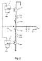
- Figure 2 illustrates a preferred embodiment according to the invention.
- the sources of both MOSFET-transistors are coupled to ground potential, so that there can be realised a simple gate control circuit resulting in rapid control.
- the operation of the preferred embodiment illustrated in figure 2 is based on the fact that by means of small transformers T3 and T4, there is formed a control signal of the current generated by the main transformer onto the gate control circuit 1.
- the current passing through the winding T1N2 renders the MOSFET M1 to conductive mode, by means of the windings T3N1 and T3N3 of the toroid T3, and simultaneously it renders the MOSFET M2 to non-conductive mode by means of the windings T4N1 and T4N3 of the toroid T4.
- the current passing through the winding T1N3 renders the transistor M2 to conductive mode by means of the windings T4N2 and T4N3 of the toroid T4, and the transistor M1 to non-conductive mode by means of the windings T3N2 and T3N3 of the toroid T3.
- the employed transformers T3 and T4 can advantageously comprise a small toroid, through which the wire coming out of the secondary winding of the mains transformer is taken, so that there is only one turn in the primary winding of the transformer T3, T4.
- control signal is not obtained with separate control transformers T3, T4, but the control signal is obtained from the third and fourth secondary windings of the mains transformer, as is illustrated in figure 3. Now the windings T1N4 and T1N5 of the mains transformer are coupled to the control circuits 1 of the MOSFET-transistors.
- FIG 4 An advantageous arrangement of the gate control circuit 1 is illustrated in figure 4.
- This type of control circuit can advantageously be used together with the preferred embodiment illustrated in figure 2.
- the control circuit is realised with two complementary bipolar transistors V1 and V2, which are connected as emitter followers. When the point-marked end of the winding T3N3/T4N3 is more positive than the emitter-connected end of the transistors V1 and V2, the transistor V1 is rendered to conductive mode, so that to the outlet of the control circuit and to the gate of the MOSFET M1, M2, there begins to flow current, whereupon the MOSFET M1, M2 is switched to conductive mode.
- the transistor V2 When the emitter-connected end of the transistors V1 and V2 of the winding T3N3/T4N3 is the more positive, the transistor V2 is rendered to conductive mode, in which case the gate charge of the MOSFET M1, M2 begins to be discharged. At the same moment, the thyristor coupling formed by the transistors V3 and V4 is triggered to conductive mode, thus remarkably speeding up the discharge of the gate charge of the MOSFET and its switching to non-conductive mode.
- the diodes D1 - D7 serve as saturation prevention diodes of the transistors V1 and V2.
- V1 When V1 is switched to conductive mode, its collector is in a higher potential - for the magnitude of two diode threshold voltages - than its base when V1 is not saturated.
- V1 When the voltage effective in relation to the transistor V1 changes polarity, V1 is rapidly rendered to non-conductive mode.
- Saturation prevention diodes reduce the transistor storage time, which forms the longest delay when switching a transistor from conductive mode to non-conductive mode.
- Figure 5 illustrates a third preferred embodiment of the invention.
- the negative outlet voltage whereof can be obtained by means of a circuit illustrated in figure 2; however, the polarity of the voltages is opposite to said figure 2, and instead of n -type MOSFET-transistors, there are used p -type MOSFET-transistors.
Applications Claiming Priority (3)
| Application Number | Priority Date | Filing Date | Title |
|---|---|---|---|
| FI964184 | 1996-10-18 | ||
| FI964184A FI114056B (fi) | 1996-10-18 | 1996-10-18 | Teholähde |
| PCT/FI1997/000632 WO1998018198A1 (en) | 1996-10-18 | 1997-10-17 | Active rectifier circuit |
Publications (2)
| Publication Number | Publication Date |
|---|---|
| EP0932929A1 EP0932929A1 (en) | 1999-08-04 |
| EP0932929B1 true EP0932929B1 (en) | 2002-08-14 |
Family
ID=8546900
Family Applications (1)
| Application Number | Title | Priority Date | Filing Date |
|---|---|---|---|
| EP97944921A Expired - Lifetime EP0932929B1 (en) | 1996-10-18 | 1997-10-17 | Active rectifier circuit |
Country Status (10)
| Country | Link |
|---|---|
| EP (1) | EP0932929B1 (pt-PT) |
| AT (1) | ATE222424T1 (pt-PT) |
| DE (1) | DE69714753T2 (pt-PT) |
| DK (1) | DK0932929T3 (pt-PT) |
| ES (1) | ES2181032T3 (pt-PT) |
| FI (1) | FI114056B (pt-PT) |
| NO (1) | NO991848L (pt-PT) |
| PL (1) | PL184963B1 (pt-PT) |
| RU (1) | RU2190293C2 (pt-PT) |
| WO (1) | WO1998018198A1 (pt-PT) |
Cited By (2)
| Publication number | Priority date | Publication date | Assignee | Title |
|---|---|---|---|---|
| US8023290B2 (en) | 1997-01-24 | 2011-09-20 | Synqor, Inc. | High efficiency power converter |
| US10199950B1 (en) | 2013-07-02 | 2019-02-05 | Vlt, Inc. | Power distribution architecture with series-connected bus converter |
Families Citing this family (2)
| Publication number | Priority date | Publication date | Assignee | Title |
|---|---|---|---|---|
| WO2001055142A1 (en) * | 2000-01-28 | 2001-08-02 | Syngenta Limited | Isothiazole derivatives and their use as pesticides |
| GB2370431A (en) * | 2000-12-19 | 2002-06-26 | Brian Victor Olliver | A dc-ac-dc power converter |
Family Cites Families (2)
| Publication number | Priority date | Publication date | Assignee | Title |
|---|---|---|---|---|
| DE3422777A1 (de) * | 1984-06-20 | 1986-01-02 | ANT Nachrichtentechnik GmbH, 7150 Backnang | Mit einer induktivitaet beschaltetes gesteuertes gleichrichterelement, sowie dessen verwendung |
| US5179512A (en) * | 1991-09-18 | 1993-01-12 | General Electric Company | Gate drive for synchronous rectifiers in resonant converters |
-
1996
- 1996-10-18 FI FI964184A patent/FI114056B/fi active
-
1997
- 1997-10-17 AT AT97944921T patent/ATE222424T1/de not_active IP Right Cessation
- 1997-10-17 RU RU99109589/09A patent/RU2190293C2/ru not_active IP Right Cessation
- 1997-10-17 PL PL97332824A patent/PL184963B1/pl not_active IP Right Cessation
- 1997-10-17 DK DK97944921T patent/DK0932929T3/da active
- 1997-10-17 EP EP97944921A patent/EP0932929B1/en not_active Expired - Lifetime
- 1997-10-17 DE DE69714753T patent/DE69714753T2/de not_active Expired - Lifetime
- 1997-10-17 ES ES97944921T patent/ES2181032T3/es not_active Expired - Lifetime
- 1997-10-17 WO PCT/FI1997/000632 patent/WO1998018198A1/en active IP Right Grant
-
1999
- 1999-04-16 NO NO991848A patent/NO991848L/no not_active Application Discontinuation
Cited By (7)
| Publication number | Priority date | Publication date | Assignee | Title |
|---|---|---|---|---|
| US8023290B2 (en) | 1997-01-24 | 2011-09-20 | Synqor, Inc. | High efficiency power converter |
| US8493751B2 (en) | 1997-01-24 | 2013-07-23 | Synqor, Inc. | High efficiency power converter |
| US9143042B2 (en) | 1997-01-24 | 2015-09-22 | Synqor, Inc. | High efficiency power converter |
| US10199950B1 (en) | 2013-07-02 | 2019-02-05 | Vlt, Inc. | Power distribution architecture with series-connected bus converter |
| US10594223B1 (en) | 2013-07-02 | 2020-03-17 | Vlt, Inc. | Power distribution architecture with series-connected bus converter |
| US11075583B1 (en) | 2013-07-02 | 2021-07-27 | Vicor Corporation | Power distribution architecture with series-connected bus converter |
| US11705820B2 (en) | 2013-07-02 | 2023-07-18 | Vicor Corporation | Power distribution architecture with series-connected bus converter |
Also Published As
| Publication number | Publication date |
|---|---|
| RU2190293C2 (ru) | 2002-09-27 |
| FI114056B (fi) | 2004-07-30 |
| DE69714753T2 (de) | 2003-04-30 |
| FI964184A (fi) | 1998-04-19 |
| WO1998018198A1 (en) | 1998-04-30 |
| DE69714753D1 (de) | 2002-09-19 |
| PL184963B1 (pl) | 2003-01-31 |
| DK0932929T3 (da) | 2002-12-16 |
| PL332824A1 (en) | 1999-10-11 |
| ES2181032T3 (es) | 2003-02-16 |
| FI964184A0 (fi) | 1996-10-18 |
| ATE222424T1 (de) | 2002-08-15 |
| NO991848D0 (no) | 1999-04-16 |
| NO316852B1 (no) | 1999-04-16 |
| EP0932929A1 (en) | 1999-08-04 |
| NO991848L (no) | 1999-04-16 |
Similar Documents
| Publication | Publication Date | Title |
|---|---|---|
| KR100852550B1 (ko) | 자기-구동 동기식 정류를 위한 방법 및 회로 | |
| US6256214B1 (en) | General self-driven synchronous rectification scheme for synchronous rectifiers having a floating gate | |
| US5471376A (en) | Low-loss active voltage-clamp circuit for single-ended forward PWM converter | |
| US9293999B1 (en) | Automatic enhanced self-driven synchronous rectification for power converters | |
| US5303138A (en) | Low loss synchronous rectifier for application to clamped-mode power converters | |
| US7564704B2 (en) | Method of forming a power supply controller and structure therefor | |
| US20140126247A1 (en) | Snubber circuit for dc-dc voltage converter | |
| US11742758B2 (en) | Boost converter and control method | |
| KR20060055415A (ko) | 영전압-영전류 스위칭을 이용한 3 레벨 직류-직류 컨버터 | |
| US6477064B1 (en) | High efficiency DC-DC power converter with turn-off snubber | |
| US5920473A (en) | Dc-to-Dc power converter with integrated magnetic power transformer | |
| US6856520B2 (en) | Double sided IGBT phase leg architecture and clocking method for reduced turn on loss | |
| Toba et al. | Auxiliary resonant commutated pole inverter using two internal voltage-points of DC source | |
| EP0932929B1 (en) | Active rectifier circuit | |
| Voss et al. | Adapted auxiliary-resonant commutated pole in the dual-active bridge | |
| EP0942520A2 (en) | DC to DC power converter | |
| Kayser et al. | Hybrid Switch with SiC MOSFET and fast IGBT for High Power Applications | |
| JP3321203B2 (ja) | 絶縁型スイッチング回路、シールド機能を持つ絶縁型スイッチング回路および絶縁型スイッチング回路 | |
| JPH07337022A (ja) | 補助共振転流回路を用いた電力変換装置 | |
| Ziemba et al. | Efficient IGBT switching | |
| JP4717621B2 (ja) | 電源回路 | |
| CN113824320A (zh) | 具有被动式无损失缓冲器的升压转换装置 | |
| JPH0223112Y2 (pt-PT) | ||
| JPH0683043B2 (ja) | スイツチング回路 | |
| Patni et al. | Optimised power stages for high frequency 380/440 VAC medium power switch mode supplies |
Legal Events
| Date | Code | Title | Description |
|---|---|---|---|
| PUAI | Public reference made under article 153(3) epc to a published international application that has entered the european phase |
Free format text: ORIGINAL CODE: 0009012 |
|
| 17P | Request for examination filed |
Effective date: 19990423 |
|
| AK | Designated contracting states |
Kind code of ref document: A1 Designated state(s): AT BE CH DE DK ES FR GB IT LI NL SE |
|
| 17Q | First examination report despatched |
Effective date: 20000127 |
|
| GRAG | Despatch of communication of intention to grant |
Free format text: ORIGINAL CODE: EPIDOS AGRA |
|
| RAP1 | Party data changed (applicant data changed or rights of an application transferred) |
Owner name: OY LEXEL FINLAND AB |
|
| GRAG | Despatch of communication of intention to grant |
Free format text: ORIGINAL CODE: EPIDOS AGRA |
|
| GRAG | Despatch of communication of intention to grant |
Free format text: ORIGINAL CODE: EPIDOS AGRA |
|
| GRAH | Despatch of communication of intention to grant a patent |
Free format text: ORIGINAL CODE: EPIDOS IGRA |
|
| GRAH | Despatch of communication of intention to grant a patent |
Free format text: ORIGINAL CODE: EPIDOS IGRA |
|
| GRAA | (expected) grant |
Free format text: ORIGINAL CODE: 0009210 |
|
| AK | Designated contracting states |
Kind code of ref document: B1 Designated state(s): AT BE CH DE DK ES FR GB IT LI NL SE |
|
| REF | Corresponds to: |
Ref document number: 222424 Country of ref document: AT Date of ref document: 20020815 Kind code of ref document: T |
|
| REG | Reference to a national code |
Ref country code: GB Ref legal event code: FG4D |
|
| REG | Reference to a national code |
Ref country code: CH Ref legal event code: EP |
|
| REG | Reference to a national code |
Ref country code: CH Ref legal event code: NV Representative=s name: E. BLUM & CO. PATENTANWAELTE |
|
| REF | Corresponds to: |
Ref document number: 69714753 Country of ref document: DE Date of ref document: 20020919 |
|
| REG | Reference to a national code |
Ref country code: DK Ref legal event code: T3 |
|
| ET | Fr: translation filed | ||
| REG | Reference to a national code |
Ref country code: ES Ref legal event code: FG2A Ref document number: 2181032 Country of ref document: ES Kind code of ref document: T3 |
|
| PLBE | No opposition filed within time limit |
Free format text: ORIGINAL CODE: 0009261 |
|
| STAA | Information on the status of an ep patent application or granted ep patent |
Free format text: STATUS: NO OPPOSITION FILED WITHIN TIME LIMIT |
|
| 26N | No opposition filed |
Effective date: 20030515 |
|
| REG | Reference to a national code |
Ref country code: CH Ref legal event code: PFA Owner name: OY LEXEL FINLAND AB Free format text: OY LEXEL FINLAND AB#OLARINLUOMA 14#02200 ESPOO (FI) -TRANSFER TO- OY LEXEL FINLAND AB#OLARINLUOMA 14#02200 ESPOO (FI) |
|
| PGFP | Annual fee paid to national office [announced via postgrant information from national office to epo] |
Ref country code: SE Payment date: 20091026 Year of fee payment: 13 Ref country code: ES Payment date: 20091022 Year of fee payment: 13 Ref country code: DK Payment date: 20091027 Year of fee payment: 13 Ref country code: DE Payment date: 20091027 Year of fee payment: 13 Ref country code: CH Payment date: 20091014 Year of fee payment: 13 Ref country code: AT Payment date: 20091027 Year of fee payment: 13 |
|
| PGFP | Annual fee paid to national office [announced via postgrant information from national office to epo] |
Ref country code: NL Payment date: 20091029 Year of fee payment: 13 |
|
| PGFP | Annual fee paid to national office [announced via postgrant information from national office to epo] |
Ref country code: IT Payment date: 20091022 Year of fee payment: 13 Ref country code: GB Payment date: 20091027 Year of fee payment: 13 Ref country code: FR Payment date: 20091110 Year of fee payment: 13 |
|
| PGFP | Annual fee paid to national office [announced via postgrant information from national office to epo] |
Ref country code: BE Payment date: 20091023 Year of fee payment: 13 |
|
| BERE | Be: lapsed |
Owner name: OY *LEXEL FINLAND A.B. Effective date: 20101031 |
|
| REG | Reference to a national code |
Ref country code: NL Ref legal event code: V1 Effective date: 20110501 |
|
| REG | Reference to a national code |
Ref country code: DK Ref legal event code: EBP |
|
| REG | Reference to a national code |
Ref country code: CH Ref legal event code: PL |
|
| GBPC | Gb: european patent ceased through non-payment of renewal fee |
Effective date: 20101017 |
|
| PG25 | Lapsed in a contracting state [announced via postgrant information from national office to epo] |
Ref country code: CH Free format text: LAPSE BECAUSE OF NON-PAYMENT OF DUE FEES Effective date: 20101031 Ref country code: FR Free format text: LAPSE BECAUSE OF NON-PAYMENT OF DUE FEES Effective date: 20101102 Ref country code: LI Free format text: LAPSE BECAUSE OF NON-PAYMENT OF DUE FEES Effective date: 20101031 |
|
| REG | Reference to a national code |
Ref country code: FR Ref legal event code: ST Effective date: 20110630 |
|
| PG25 | Lapsed in a contracting state [announced via postgrant information from national office to epo] |
Ref country code: BE Free format text: LAPSE BECAUSE OF NON-PAYMENT OF DUE FEES Effective date: 20101031 Ref country code: AT Free format text: LAPSE BECAUSE OF NON-PAYMENT OF DUE FEES Effective date: 20101017 Ref country code: NL Free format text: LAPSE BECAUSE OF NON-PAYMENT OF DUE FEES Effective date: 20110501 Ref country code: GB Free format text: LAPSE BECAUSE OF NON-PAYMENT OF DUE FEES Effective date: 20101017 |
|
| PG25 | Lapsed in a contracting state [announced via postgrant information from national office to epo] |
Ref country code: SE Free format text: LAPSE BECAUSE OF NON-PAYMENT OF DUE FEES Effective date: 20101018 |
|
| REG | Reference to a national code |
Ref country code: DE Ref legal event code: R119 Ref document number: 69714753 Country of ref document: DE Effective date: 20110502 |
|
| PG25 | Lapsed in a contracting state [announced via postgrant information from national office to epo] |
Ref country code: DK Free format text: LAPSE BECAUSE OF NON-PAYMENT OF DUE FEES Effective date: 20101031 |
|
| REG | Reference to a national code |
Ref country code: ES Ref legal event code: FD2A Effective date: 20111121 |
|
| PG25 | Lapsed in a contracting state [announced via postgrant information from national office to epo] |
Ref country code: IT Free format text: LAPSE BECAUSE OF NON-PAYMENT OF DUE FEES Effective date: 20101017 |
|
| PG25 | Lapsed in a contracting state [announced via postgrant information from national office to epo] |
Ref country code: ES Free format text: LAPSE BECAUSE OF NON-PAYMENT OF DUE FEES Effective date: 20101018 |
|
| PG25 | Lapsed in a contracting state [announced via postgrant information from national office to epo] |
Ref country code: DE Free format text: LAPSE BECAUSE OF NON-PAYMENT OF DUE FEES Effective date: 20110502 |