EP0177108A1 - Opto-electronic focussing-error detection system - Google Patents
Opto-electronic focussing-error detection system Download PDFInfo
- Publication number
- EP0177108A1 EP0177108A1 EP85201588A EP85201588A EP0177108A1 EP 0177108 A1 EP0177108 A1 EP 0177108A1 EP 85201588 A EP85201588 A EP 85201588A EP 85201588 A EP85201588 A EP 85201588A EP 0177108 A1 EP0177108 A1 EP 0177108A1
- Authority
- EP
- European Patent Office
- Prior art keywords
- detection system
- focussing
- plane
- radiation
- detectors
- Prior art date
- Legal status (The legal status is an assumption and is not a legal conclusion. Google has not performed a legal analysis and makes no representation as to the accuracy of the status listed.)
- Granted
Links
Images

Classifications
-
- G—PHYSICS
- G02—OPTICS
- G02B—OPTICAL ELEMENTS, SYSTEMS OR APPARATUS
- G02B27/00—Optical systems or apparatus not provided for by any of the groups G02B1/00 - G02B26/00, G02B30/00
- G02B27/10—Beam splitting or combining systems
-
- G—PHYSICS
- G11—INFORMATION STORAGE
- G11B—INFORMATION STORAGE BASED ON RELATIVE MOVEMENT BETWEEN RECORD CARRIER AND TRANSDUCER
- G11B7/00—Recording or reproducing by optical means, e.g. recording using a thermal beam of optical radiation by modifying optical properties or the physical structure, reproducing using an optical beam at lower power by sensing optical properties; Record carriers therefor
- G11B7/12—Heads, e.g. forming of the optical beam spot or modulation of the optical beam
- G11B7/135—Means for guiding the beam from the source to the record carrier or from the record carrier to the detector
- G11B7/1381—Non-lens elements for altering the properties of the beam, e.g. knife edges, slits, filters or stops
-
- G—PHYSICS
- G02—OPTICS
- G02B—OPTICAL ELEMENTS, SYSTEMS OR APPARATUS
- G02B27/00—Optical systems or apparatus not provided for by any of the groups G02B1/00 - G02B26/00, G02B30/00
- G02B27/10—Beam splitting or combining systems
- G02B27/14—Beam splitting or combining systems operating by reflection only
- G02B27/143—Beam splitting or combining systems operating by reflection only using macroscopically faceted or segmented reflective surfaces
-
- G—PHYSICS
- G02—OPTICS
- G02B—OPTICAL ELEMENTS, SYSTEMS OR APPARATUS
- G02B27/00—Optical systems or apparatus not provided for by any of the groups G02B1/00 - G02B26/00, G02B30/00
- G02B27/10—Beam splitting or combining systems
- G02B27/14—Beam splitting or combining systems operating by reflection only
- G02B27/144—Beam splitting or combining systems operating by reflection only using partially transparent surfaces without spectral selectivity
-
- G—PHYSICS
- G11—INFORMATION STORAGE
- G11B—INFORMATION STORAGE BASED ON RELATIVE MOVEMENT BETWEEN RECORD CARRIER AND TRANSDUCER
- G11B7/00—Recording or reproducing by optical means, e.g. recording using a thermal beam of optical radiation by modifying optical properties or the physical structure, reproducing using an optical beam at lower power by sensing optical properties; Record carriers therefor
- G11B7/08—Disposition or mounting of heads or light sources relatively to record carriers
- G11B7/09—Disposition or mounting of heads or light sources relatively to record carriers with provision for moving the light beam or focus plane for the purpose of maintaining alignment of the light beam relative to the record carrier during transducing operation, e.g. to compensate for surface irregularities of the latter or for track following
- G11B7/0908—Disposition or mounting of heads or light sources relatively to record carriers with provision for moving the light beam or focus plane for the purpose of maintaining alignment of the light beam relative to the record carrier during transducing operation, e.g. to compensate for surface irregularities of the latter or for track following for focusing only
- G11B7/0916—Foucault or knife-edge methods
Definitions
- the invention relates to an opto-electronic focussing-error detection system for detecting, in an optical imaging system, a deviation between a radiation-reflecting surface and a focussing plane of an objective system, in particular for an apparatus for reading a record carrier having an optical radiation-reflecting information structure or an apparatus for optically recording information in a record carrier,
- focussing-error detection system comprises a beam-splitting element, arranged in the path of a radiation beam which has been reflected by the reflecting surface, and a radiation-sensitive detection system, arranged behind the beam-splitting element and comprising a plurality of detectors arranged in two groups of which a first group is associated with a first sub-beam and a second group with a second sub-beam of two sub-beams formed by the beam-splitting element, the outputs of the detectors being connected to the inputs of an electronic circuit which derives a focussing-error signal from the detector signals.
- Such a system is known, inter alia from Netherlands Patent Application no. 81 04588 (PHN 10.173) which has been laid open to public inspection.
- the system described therein comprises a radiation source in the form of a semiconductor diode laser.
- An objective system focusses the read beam emitted by this laser onto an information structure on a disc-shaped record carrier.
- the read beam which has been reflected by the information structure traverses the objective system a second time and subsequently passes through a beam-dividing prism arranged between the radiation source and the objective system. This prism divides the modulated read beam from the radiation path of the beam which has been emitted by the source, so that the modulated beam can be received by a
- radiation-sensitive detection system which supplies an electric signal in conformity with the modulation of the latter beam.
- a roof prism may be arranged on the exit surface of the beam dividing prism. This roof prism splits the beam into two sub beams which are incident on two separate detectors of the radiation-sensitive detection system.
- This system comprises, for example, four radiation-sensitive detectors arranged along a line transverse to the refractive edge of the roof prism. Subtracting the sum of the signals from the two inner detectors from the sum of the signals from the two outer detectors yields a signal which is proportional to the focussing error.
- the beam-splitting element which should be arranged in the radiation path between the beam-dividing element and the detection system, may comprise a wedge-shaped element having the same shape as the roof prism.
- This wedge-shaped element may be made of a cheap plastics and can be manufactured cheaply using the customary moulding techniques.
- such an element is sensitive to environmental influences such as temperature.
- a temperature variation causes the refractive index and the shape of this element to change so that the sub-beams and hence the radiation spots formedby these sub-beams in the plane of the radiation-sensitive detection system are shifted relative to the associated detectors.
- this shift would be in the same direction as the shift caused by focussing errors.
- the shift of the radiation spots caused by the temperature variation is then interpreted as a focussing error, the focussing servo-system responding to it and producing incorrect focussing.
- the present invention aims at providing a focussing-error detection system comprising a beam-splitting element which subsstantially eliminates environmental influences on the focussing-error signal.
- the system is characterized in that the beam-splitting element is a compound wedge comprising two wedge sections having a common surface and each having an upper surface situated opposite said base surface, which upper surfaces are inclined relative to each other in the plane of the interface between the two wedge sections, the plane of said interface extending substantially perpendicularly to the base surface and to the upper surfaces and containing the optical axis of the imaging system, and in that the two groups of detectors are situated on opposite sides of a plane containing the optical axis and extending substantially perpendicularly to the interface.
- the invention may also be employed in a focussing-error detection system in which the beam-splitting element in the form of a roof prism is arranged on the beam-dividing element in the form of, for example, a prism.
- the optical behaviour of such a roof prism will also depend on, for example, the ambient temperature if this prism, is not as in the system in accordance with Netherlands Patent Application no. 81 04588 (PHN 10.173) made of a thin layer of a polymerisable plastics in which changes in the refractive index and shape as a result of temperature changes substantially compensate for each other.
- the beam-splitting element and the beam-dividing element are separated from etach other, the latter may be an element other than a prism.
- a semitransparent mirror as beam-dividing element.
- the mirror For a convergent beam which traverses this mirror the mirror constitutes a plane-parallel plate which may give rise to astigmatism because of its oblique position in the beam.
- the compound wedge is arranged on a surface of a cylindrical lens. This cylindrical lens can correct the astigmatism introduced by the plane-parallel plate.
- the compound wedge and the cylindrical lens are made of the same material and constitute one integrated optical element.
- This element can be manufactured cheaply using the customary moulding techniques.
- the strip separating the detectors of the first group extends at a first small angle and the strip separating the detectors of the second group extends at a second small angle, which is oriented oppositely to the first angle, relative to a line obtained by projecting the interface of the compound wedge onto the plane of the detection system.
- the centres of the radiation spots ean always be positioned symmetrically relative to the associated detectors in the case of correct focussing.
- the read beam is reflected by the information structure and, as the record carrier moves relative to the read beam, the reflected beam is time-modulated in conformity with the information in the record carrier.
- a beam-dividing element for example a semi-transparent mirror 6, is arranged in the radiation path from the radiation source to the collimator lens 4.
- This mirror reflects a part of the radiation emitted by the source 3 to the record carrier and transmits a part of the radiation reflected by the record carrier to a radiation-sensitive detection system 7 which converts the modulated read beam into an electric signal.
- this mirror has a reflection coefficient of the order of 0.3 so that, if losses in the radiation path are ignored about 21% of the radiation emitted by the source is incident on the detection system and only 9% returns to the radiation source.
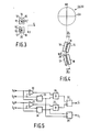
- a compound wedge 8 is arranged in the radiation path, an example of such a wedge being shown in perspective and on an enlarged scale in Fig. 2.
- This wedge comprises two wedge-sections 9 and 10 whose upper surfaces 12 and 13 are inclined oppositely relative to the common base surface 14. Alternatively, one of the upper surfaces may extend parallel to the'base surface 14 whilst the other upper surface is inclined relative to the base surface.
- the plane 11 is the interface of the two wedge sections.
- the optical axis of the imaging system represented by the dash-dot line a in Fig. 1, is situated in the plane of this interface.
- the compound wedge splits the beam b returning from the record into two sub-beams b 1 and b 2 which are deviated in opposite directions as a result of the opposite inclinations of the two wedge sections.
- the sub-beam b2 is focussed in point F 2 which is situated, for example, before the plane of drawing in Fig. 1, whilst the sub-beam b 1 is focussed in point F 1 which is situated behind the plane of drawing.
- F is the point in which the beam b would be focussed in the absence of the compound wedge.
- the detection system7 is shown slightly below points F 1 and F 2 . In reality, this system is situated in the plane containing points F 1 and F 2 and extending transversely of the optical axis.
- the detection system 7 comprises four detectors arranged in two groups of two, one group being situated, for example, before the plane of drawing in Fig. 1 and the second group behind this plane.
- Fig. 3 is a plan view of the detection system comprising the detectors 15, 16, 17 and 18 in the situation in which the beam b is focussed correctly on the plane of the information structure.
- the radiation spots V 1 . and V 2 formed by the sub-beams b 1 and b respectively are then situated symmetrically relative to the associated detectors 15, 16 and 17, 18, respectively.
- each of the radiation spots will be enlarged asymmetrically so that the centre of its radiation distribution is shifted relative to the associated detectors.
- the centres of the radiation spots of the two groups also move in opposite directions.
- the radiation spot V 1 is shifted towards the detector 15 and the radiation spot b towards the detector 17, as indicated by the broken lines V 1 ' and V 2 ' in Fig. 3.
- the detectors 15 and 17 then receive more radiation than the detectors 16 and 18. If the beam b is focussed in a point situated below the plane of the information structure, the situation is reversed and the detectors 16 and 18 receive more radiation than the detectors 15 and 17.
- This information signal is given by:
- the above focussing error signal S f may be influenced by contamination of the optical elements in the course of time or by defects in the plane of the information structure, referred to as "drop-outs". Moreover, the focussing-error signal may be influenced by tracking errors. Therefore, preferably a normalised focussing-error signal is generated which is not affected by the said events.
- This focussing-error signal is given by: This signal is independent of the total radiation intensity in the plane of the radiation-sensitive detection system and is only a function of the radiation distribution among the individual detectors.
- the signal S f ' can be derived from the detection signals by means of known electronic circuits.
- Fig. 5 shows schematically an example of a signal-processing arrangement. The circuit arrangement comprises two subtractor circuits 30 and 31, four adder circuits 32, 33, 34 and 35, and two divider circuits 3 6 and 37 and requires no further explanation.
- a cylindrical lens is arranged in the radiation path behind the semitransparent mirror 6.
- the semitransparent mirror takes the form of a plane-parallel plate which is traversed by the convergent-beam and which may render it astigmatic because this plate is arranged obliquely in the convergent beam.
- a cylindrical lens is also an astigmatic element.By a suitable choice of the relevant parameters of this lens, such as the radius of curvature of the curved lenssurface. such a lens is capable of eliminating the astigmatism introduced by the mirror.
- the cylindrical lens bears the reference numeral 21. This lens may have a plane surface 22 and a curved surface 23.
- the lens 21 may have two curved surfaces, chosen to provide cylindrical-lens action.
- the axis of the cylindrical lens extends transversely to the local optical axis a and, in the present example in which the cylindrical lens is a negative lens, it extends parallel to the plane of drawing in Fig. 1, thus coinciding with the x-axis in Pigs. 1 and 2. If a positive cylindrical lens were used, the axis of this lens would coincide with the y-axis.
- the cylindrical lens and the compound wedge may be separate elements and may be made of different materials. However, preferably these elements are made of the same material and are combined to form one integrated optical element. In that case the compound wedge need not be arranged on a separate support and, which is more important, the two elements can be manufactured together so that automatically their alignment relative to each other is correct.
- the integrated element may be made of a transparent plastics, such as polymethyl-methacrylate (PMMA) or polycarbonate (PC) and can be manufactured cheaply using known moulding techniques and dies.
- the integrated element (8, 21) may have a circular shape.
- this element is then as shown in the upper part of Fig. 4.
- CA is the cylinder axis and WA the wedge axis, i.e. the line of intersection of the interface 11 of the wedge with the upper surface 22 of the cylindrical lens.
- WA t is the projection of the wedge axis in the plane of the detectors.
- the longitudinal directions of the separating strips 19 and 20 make small angles ⁇ 1 and ⁇ 2 , respectively, of the order of 10° with the line WA'.
- the connecting line between the radiation spots V 1 and V 2 is offset relative to the separating strips 19 and 20, it is not possible to position the radiation spots for correct focussing symmetrically relative to the detectors 15, 16 and 17, 18 respectively during assembly of the focussing-error detection system by shifting the radiation spots and the substrate carrying the detectors relative to each other in two mutually perpendicular directions.
- this interface preferably extends effectively parallel to the track directions, i.e. this interface should extend perpendicularly to the plane of drawing in Fig. 1 or parallel to the y-direction in Fig. 2.
- the detectors 15, 16, 17 and 18 may then be used for generating a tracking signal which provides an indication of the degree of coincidence of the centre of the read spot V with the track centre.
- This tracking signal S is given by
- the invention has been described for a system used in an optical read unit, but the invention may also be used in a write unit or in a combined read/write unit.
- the write unit is of a construction similar to the construction of the read unit described herein.
- the radiation source in the write may be a gas laser, such as a HeNe laser, and a modulator such as an electro-optical or an acousto-optical modulator should be arranged in the path of the write beam.
- a diode laser may be used, in which case the write beam is modulated by varying the electric current in the diode laser, so that no separate modulator is needed.
- the focussing-error detection system described does not utilize any special properties of the optical information structure or surface on which the beam must be focussed. It is merely necessary that this surface is radiation-reflecting. Therefore,the focussing-error detection system may be used in various apparatus in which very accurate focussing is required, for example in microscopes.
Abstract
Description
- The invention relates to an opto-electronic focussing-error detection system for detecting, in an optical imaging system, a deviation between a radiation-reflecting surface and a focussing plane of an objective system, in particular for an apparatus for reading a record carrier having an optical radiation-reflecting information structure or an apparatus for optically recording information in a record carrier, which focussing-error detection system comprises a beam-splitting element, arranged in the path of a radiation beam which has been reflected by the reflecting surface, and a radiation-sensitive detection system, arranged behind the beam-splitting element and comprising a plurality of detectors arranged in two groups of which a first group is associated with a first sub-beam and a second group with a second sub-beam of two sub-beams formed by the beam-splitting element, the outputs of the detectors being connected to the inputs of an electronic circuit which derives a focussing-error signal from the detector signals.
- Such a system is known, inter alia from Netherlands Patent Application no. 81 04588 (PHN 10.173) which has been laid open to public inspection. The system described therein comprises a radiation source in the form of a semiconductor diode laser. An objective system focusses the read beam emitted by this laser onto an information structure on a disc-shaped record carrier. The read beam which has been reflected by the information structure traverses the objective system a second time and subsequently passes through a beam-dividing prism arranged between the radiation source and the objective system. This prism divides the modulated read beam from the radiation path of the beam which has been emitted by the source, so that the modulated beam can be received by a
- radiation-sensitive detection system which supplies an electric signal in conformity with the modulation of the latter beam.
- In optical systems which are used for imaging very minute information details and which have a large numerical aperture the depth of focus is small. For imaging systems of this type, which are employed, for example, in microscopes, or in apparatus for reading an optical record carrier with very small details, or in apparatus for recording information in a record carrier, it is essential that a deviation between the actual and the desired plane of focussing can be detected to enable the focussing to be corrected accordingly. For this purpose, as described in the afore-mentioned Netherlands Patent Application no. 81 04588, a roof prism may be arranged on the exit surface of the beam dividing prism. This roof prism splits the beam into two sub beams which are incident on two separate detectors of the radiation-sensitive detection system. This system comprises, for example, four radiation-sensitive detectors arranged along a line transverse to the refractive edge of the roof prism. Subtracting the sum of the signals from the two inner detectors from the sum of the signals from the two outer detectors yields a signal which is proportional to the focussing error.
- In practice it may be desirable to separate the beam-splitting element from the beam-dividing element, for example if for reasons of cost an element other than the prism is to be used for beam-dividing. This other element may be, for example, a semitransparent mirror. The beam-splitting element, which should be arranged in the radiation path between the beam-dividing element and the detection system, may comprise a wedge-shaped element having the same shape as the roof prism. This wedge-shaped element may be made of a cheap plastics and can be manufactured cheaply using the customary moulding techniques. However, such an element is sensitive to environmental influences such as temperature. A temperature variation causes the refractive index and the shape of this element to change so that the sub-beams and hence the radiation spots formedby these sub-beams in the plane of the radiation-sensitive detection system are shifted relative to the associated detectors. In the case of the beam-splitting element and detector arrangement described in Netherlands Patent Application no. 81 04588 this shift would be in the same direction as the shift caused by focussing errors. The shift of the radiation spots caused by the temperature variation is then interpreted as a focussing error, the focussing servo-system responding to it and producing incorrect focussing.
- The present invention aims at providing a focussing-error detection system comprising a beam-splitting element which subsstantially eliminates environmental influences on the focussing-error signal. According to the invention the system is characterized in that the beam-splitting element is a compound wedge comprising two wedge sections having a common surface and each having an upper surface situated opposite said base surface, which upper surfaces are inclined relative to each other in the plane of the interface between the two wedge sections, the plane of said interface extending substantially perpendicularly to the base surface and to the upper surfaces and containing the optical axis of the imaging system, and in that the two groups of detectors are situated on opposite sides of a plane containing the optical axis and extending substantially perpendicularly to the interface.
- In this focussing-error detection system a variation of, for example, the ambient temperature gives rise to a shift of a radiation spot in the longitudinal direction of a strip separating the detectors in one group. This shift hardly affects the difference between the output signals of the detectors of a group and consequently does not give rise to an erroneous focussing-error signal.
- The invention may also be employed in a focussing-error detection system in which the beam-splitting element in the form of a roof prism is arranged on the beam-dividing element in the form of, for example, a prism. The optical behaviour of such a roof prism will also depend on, for example, the ambient temperature if this prism, is not as in the system in accordance with Netherlands Patent Application no. 81 04588 (PHN 10.173) made of a thin layer of a polymerisable plastics in which changes in the refractive index and shape as a result of temperature changes substantially compensate for each other.
- As already stated, if the beam-splitting element and the beam-dividing element are separated from etach other, the latter may be an element other than a prism. For reasons of cost it is preferred to-use a semitransparent mirror as beam-dividing element. For a convergent beam which traverses this mirror the mirror constitutes a plane-parallel plate which may give rise to astigmatism because of its oblique position in the beam. In order to mitigate this problem a preferred embodiment of the invention is characterized further in that the compound wedge is arranged on a surface of a cylindrical lens. This cylindrical lens can correct the astigmatism introduced by the plane-parallel plate.
- Preferably, the compound wedge and the cylindrical lens are made of the same material and constitute one integrated optical element. This element can be manufactured cheaply using the customary moulding techniques.
- Preferably, the strip separating the detectors of the first group extends at a first small angle and the strip separating the detectors of the second group extends at a second small angle, which is oriented oppositely to the first angle, relative to a line obtained by projecting the interface of the compound wedge onto the plane of the detection system. Thus, by moving the radiation-sensitive detection system relative to the sub-beams in two mutually perpendicular directions, the centres of the radiation spots ean always be positioned symmetrically relative to the associated detectors in the case of correct focussing.
- Embodiments of the invention, used in an apparatus for reading an optical record carrier, will now be described in more detail, by way of example with reference to the accompanying drawings. In the drawings:
- Fig. 1 shows schematically a read apparatus equipped with a focussing-error detection system in accordance with the invention,
- Fig. 2 is a perspective view of an example of the beam-splitting element used iv said apparatus,
- Fig. 3 is a plan view of the radiation-sensitive detection system employed in the apparatus,
- Fig. 4 is a plan view of the beam-splitting element, showing the arrangement of the detectors relative to the interface of the wedge, and
- Fig. 5 shows a circuit arrangement for processing the detector signals into a focussing-error signal.
- Fig. 1 shows a small part of a disc-shaped record carrier 1 in radial cross-section. The radiation-reflecting information structure is situated on the upper side of the record carrier and comprises a multitude of information areas, not shown, arranged along information tracks 2. The information structure is scanned by a read beam b produced by a radiation source 3, for example, a semiconductor-diode laser. A
collimator lens 4 converts the diverging beam into a parallel beam of such a cross-section that the pupil of anobjective system 5 is filled correctly. This objective system forms a radiation spot V of minimal dimensions on the information structure. - The read beam is reflected by the information structure and, as the record carrier moves relative to the read beam, the reflected beam is time-modulated in conformity with the information in the record carrier. In order to separate the modulated beam from the beam emitted by the radiation source a beam-dividing element, for example a
semi-transparent mirror 6, is arranged in the radiation path from the radiation source to thecollimator lens 4. This mirror reflects a part of the radiation emitted by the source 3 to the record carrier and transmits a part of the radiation reflected by the record carrier to a radiation-sensitive detection system 7 which converts the modulated read beam into an electric signal. Preferably, this mirror has a reflection coefficient of the order of 0.3 so that, if losses in the radiation path are ignored about 21% of the radiation emitted by the source is incident on the detection system and only 9% returns to the radiation source. - In order to generate a focussing-error signal which provides an indication of the magnitude and the direction of a deviation between the plane of focussing of the objective system and the plane of the information structure, a
compound wedge 8 is arranged in the radiation path, an example of such a wedge being shown in perspective and on an enlarged scale in Fig. 2. This wedge comprises two wedge-sections upper surfaces plane 11 is the interface of the two wedge sections. The optical axis of the imaging system, represented by the dash-dot line a in Fig. 1, is situated in the plane of this interface. - The compound wedge splits the beam b returning from the record into two sub-beams b1 and b2 which are deviated in opposite directions as a result of the opposite inclinations of the two wedge sections. The sub-beam b2 is focussed in point F2 which is situated, for example, before the plane of drawing in Fig. 1, whilst the sub-beam b1 is focussed in point F1 which is situated behind the plane of drawing. F is the point in which the beam b would be focussed in the absence of the compound wedge. For the sake of clarity the detection system7 is shown slightly below points F1 and F2. In reality, this system is situated in the plane containing points F1 and F2 and extending transversely of the optical axis.
- The detection system 7 comprises four detectors arranged in two groups of two, one group being situated, for example, before the plane of drawing in Fig. 1 and the second group behind this plane. Fig. 3 is a plan view of the detection system comprising the
detectors detectors - When the beam b is focussed at a point situated above the plane of the information structure the radiation spot V1 is shifted towards the
detector 15 and the radiation spot b towards thedetector 17, as indicated by the broken lines V1' and V2' in Fig. 3. Thedetectors detectors detectors detectors - If the output signals of the
detectors -


- If the detectors are not positioned correctly the above focussing error signal Sf may be influenced by contamination of the optical elements in the course of time or by defects in the plane of the information structure, referred to as "drop-outs". Moreover, the focussing-error signal may be influenced by tracking errors. Therefore, preferably a normalised focussing-error signal is generated which is not affected by the said events. This focussing-error signal is given by:

subtractor circuits adder circuits divider circuits - Preferably, a cylindrical lens is arranged in the radiation path behind the
semitransparent mirror 6. The semitransparent mirror takes the form of a plane-parallel plate which is traversed by the convergent-beam and which may render it astigmatic because this plate is arranged obliquely in the convergent beam. A cylindrical lens is also an astigmatic element.By a suitable choice of the relevant parameters of this lens, such as the radius of curvature of the curved lenssurface. such a lens is capable of eliminating the astigmatism introduced by the mirror. In Figs. 1 and 2 the cylindrical lens bears thereference numeral 21. This lens may have aplane surface 22 and acurved surface 23. Alternatively, thelens 21 may have two curved surfaces, chosen to provide cylindrical-lens action. The axis of the cylindrical lens extends transversely to the local optical axis a and, in the present example in which the cylindrical lens is a negative lens, it extends parallel to the plane of drawing in Fig. 1, thus coinciding with the x-axis in Pigs. 1 and 2. If a positive cylindrical lens were used, the axis of this lens would coincide with the y-axis. - The cylindrical lens and the compound wedge may be separate elements and may be made of different materials. However, preferably these elements are made of the same material and are combined to form one integrated optical element. In that case the compound wedge need not be arranged on a separate support and, which is more important, the two elements can be manufactured together so that automatically their alignment relative to each other is correct. The integrated element may be made of a transparent plastics, such as polymethyl-methacrylate (PMMA) or polycarbonate (PC) and can be manufactured cheaply using known moulding techniques and dies.
- The optical behaviour of elements made of such plastics is temperature-dependent, but because in the present arrangement the change in refractive index of the material as a result of a temperature variation gives rise to a displacement of the radiation spots V1 and V2 in the longitudinal direction of the separating strips 19 and 20, i.e. in the y-direction in Fig. 2, these changes will not affect the focussing-error signal.
- Instead of the rectangular shape shown in Fig. 2 the integrated element (8, 21) may have a circular shape. In plan view this element is then as shown in the upper part of Fig. 4. In this Figure CA is the cylinder axis and WA the wedge axis, i.e. the line of intersection of the
interface 11 of the wedge with theupper surface 22 of the cylindrical lens. The lower part of Fig. 4 shows how the detectors are preferably oriented relative to the wedge axis. WAt is the projection of the wedge axis in the plane of the detectors. The longitudinal directions of the separating strips 19 and 20 make small angles β1 and β2, respectively, of the order of 10° with the line WA'. If the connecting line between the radiation spots V1 and V2 is offset relative to the separating strips 19 and 20, it is not possible to position the radiation spots for correct focussing symmetrically relative to thedetectors - For the actual focussing-error detection the orientation of the
wedge interface 11 is irrelevant. It is important only that the plane of this interface contained the optical axis a. When the focussing-error detection system is employed in an apparatus for reading an optical record carrier, this interface preferably extends effectively parallel to the track directions, i.e. this interface should extend perpendicularly to the plane of drawing in Fig. 1 or parallel to the y-direction in Fig. 2. Thedetectors 
- The invention has been described for a system used in an optical read unit, but the invention may also be used in a write unit or in a combined read/write unit. The write unit is of a construction similar to the construction of the read unit described herein. For recording information, for example by melting pits into a metal layer, more power is required than for reading and, moreover, the write beam should be time-modulated in conformity with the information to be recorded. The radiation source in the write may be a gas laser, such as a HeNe laser, and a modulator such as an electro-optical or an acousto-optical modulator should be arranged in the path of the write beam. Alternatively, a diode laser may be used, in which case the write beam is modulated by varying the electric current in the diode laser, so that no separate modulator is needed.
- The focussing-error detection system described does not utilize any special properties of the optical information structure or surface on which the beam must be focussed. It is merely necessary that this surface is radiation-reflecting. Therefore,the focussing-error detection system may be used in various apparatus in which very accurate focussing is required, for example in microscopes.
Claims (5)
Applications Claiming Priority (2)
| Application Number | Priority Date | Filing Date | Title |
|---|---|---|---|
| NL8403034 | 1984-10-05 | ||
| NL8403034A NL8403034A (en) | 1984-10-05 | 1984-10-05 | OPTO-ELECTRONIC FOCUS ERROR DETECTION SYSTEM. |
Publications (2)
| Publication Number | Publication Date |
|---|---|
| EP0177108A1 true EP0177108A1 (en) | 1986-04-09 |
| EP0177108B1 EP0177108B1 (en) | 1989-04-19 |
Family
ID=19844567
Family Applications (1)
| Application Number | Title | Priority Date | Filing Date |
|---|---|---|---|
| EP85201588A Expired EP0177108B1 (en) | 1984-10-05 | 1985-10-02 | Opto-electronic focussing-error detection system |
Country Status (11)
| Country | Link |
|---|---|
| US (1) | US4712205A (en) |
| EP (1) | EP0177108B1 (en) |
| JP (1) | JPS61105737A (en) |
| KR (1) | KR920010949B1 (en) |
| AU (1) | AU571741B2 (en) |
| CA (1) | CA1330495C (en) |
| DE (1) | DE3569621D1 (en) |
| ES (1) | ES8609746A1 (en) |
| HK (1) | HK83991A (en) |
| NL (1) | NL8403034A (en) |
| SG (1) | SG89690G (en) |
Cited By (12)
| Publication number | Priority date | Publication date | Assignee | Title |
|---|---|---|---|---|
| EP0236137A2 (en) * | 1986-03-05 | 1987-09-09 | Chelsea Instruments Limited | Novel beam splitter and spectrometer containing the beam splitter |
| EP0316866A2 (en) * | 1987-11-17 | 1989-05-24 | Kabushiki Kaisha Toshiba | Apparatus for detecting a focusing state of optical system |
| EP0317536A2 (en) * | 1987-11-13 | 1989-05-24 | International Business Machines Corporation | Employing the principles of separability for detecting light beams |
| EP0390116A2 (en) * | 1989-03-31 | 1990-10-03 | Kabushiki Kaisha Toshiba | Optical information processing system |
| EP0454854A1 (en) * | 1989-10-14 | 1991-11-06 | Copal Company Limited | Optical pickup apparatus comprising a focus adjusting apparatus |
| US5326677A (en) * | 1993-02-19 | 1994-07-05 | Eastman Kodak Company | Optical retrieval apparatus using a tellurium (IV) leuco dye |
| US5353272A (en) * | 1992-12-29 | 1994-10-04 | Eastman Kodak Company | Apparatus and method for a modified half-aperture focus/tracking/data sensor system |
| US5360970A (en) * | 1992-12-29 | 1994-11-01 | Eastman Kodak Company | Apparatus and method for a single return path signal sensor system |
| US5406541A (en) * | 1992-12-29 | 1995-04-11 | Eastman Kodak Company | Apparatus and method for a dual half-aperture focus sensor system |
| US5491675A (en) * | 1994-06-14 | 1996-02-13 | Eastman Kodak Company | Single return path orthogonally-arranged optical focus and tracking sensor system |
| US7808617B2 (en) | 2007-09-17 | 2010-10-05 | Quality Vision International, Inc. | Dual resolution, dual range sensor system and method |
| US9663740B2 (en) | 2004-04-06 | 2017-05-30 | Akzo Nobel N.V. | Polymeric imides as pour point depressant additives for oil compositions |
Families Citing this family (18)
| Publication number | Priority date | Publication date | Assignee | Title |
|---|---|---|---|---|
| NL8702245A (en) * | 1987-09-21 | 1989-04-17 | Philips Nv | DEVICE FOR SCANNING A RADIATION-REFLECTING INFORMATION SHEET WITH OPTICAL RADIATION. |
| US5161139A (en) * | 1989-01-06 | 1992-11-03 | Kabushiki Kaisha Toshiba | Focusing error detecting apparatus |
| US4987292A (en) * | 1989-06-12 | 1991-01-22 | Digital Equipment Corporation | Method and apparatus for detecting focus and tracking errors |
| US5182444A (en) * | 1989-06-12 | 1993-01-26 | Digital Equipment Corporation | Split lens displaced long from each other along plane of cut |
| JP2591302B2 (en) * | 1990-09-26 | 1997-03-19 | 松下電器産業株式会社 | Focus error detection device |
| JPH04364231A (en) * | 1991-01-07 | 1992-12-16 | Toshiba Corp | Optical head device |
| JPH0554409A (en) * | 1991-08-27 | 1993-03-05 | Nikon Corp | Focus detecting optical system |
| US5241523A (en) * | 1991-12-05 | 1993-08-31 | Eastman Kodak Company | Polarization-based auto-focus apparatus |
| US5446710A (en) * | 1992-11-06 | 1995-08-29 | International Business Machines Corporation | Focus error detection using an equal path length lateral shearing interferometer |
| US5607739A (en) * | 1995-03-07 | 1997-03-04 | Eastman Kodak Company | Temperature sensor and method for optical disk |
| JP2874663B2 (en) * | 1996-09-06 | 1999-03-24 | 日本電気株式会社 | Optical head focus error detection method |
| US5761162A (en) * | 1996-10-31 | 1998-06-02 | Eastman Kodak Company | Multi-element prism for optical heads |
| US5793719A (en) * | 1996-10-31 | 1998-08-11 | Eastman Kodak Company | Multi-element prism for optical heads |
| JP3708320B2 (en) * | 1998-02-04 | 2005-10-19 | 富士通株式会社 | Optical information detector |
| US6483650B1 (en) * | 1998-08-04 | 2002-11-19 | Sony Corporation | Integrated optical element, optical pickup, and optical disk device |
| KR100301572B1 (en) * | 1999-04-28 | 2001-09-26 | 김영수 | an optoelectronic switch |
| US7480219B2 (en) * | 2000-11-21 | 2009-01-20 | Lg Electronics Inc. | Method and apparatus for calculating a variation per track of a focus error to control the tilt of a disk |
| US9664909B1 (en) | 2012-07-11 | 2017-05-30 | Kla-Tencor Corporation | Monolithic optical beam splitter with focusing lens |
Citations (5)
| Publication number | Priority date | Publication date | Assignee | Title |
|---|---|---|---|---|
| US3971002A (en) * | 1973-06-29 | 1976-07-20 | Thomson-Brandt | Device for the optical read-out of a diffractive track belonging to a data carrier in the form of a disc or tape |
| FR2313716A1 (en) * | 1975-06-03 | 1976-12-31 | Thomson Brandt | OPTICAL READING SYSTEM BY REFLECTION OF AN INFORMATION MEDIA |
| DE2846696A1 (en) * | 1977-10-27 | 1979-05-03 | Asahi Optical Co Ltd | DEVICE FOR FOCUSING DETECTION |
| US4296316A (en) * | 1978-12-25 | 1981-10-20 | Tokyo Shibaura Denki Kabushiki Kaisha | Optical focusing device |
| GB2120493A (en) * | 1982-05-19 | 1983-11-30 | Philips Nv | Opto-electronic focusing-error detection device |
Family Cites Families (8)
| Publication number | Priority date | Publication date | Assignee | Title |
|---|---|---|---|---|
| JPS5148335A (en) * | 1974-10-23 | 1976-04-26 | Miranda Kamera Kk | Sotsukyobu osonaeta shotenban |
| US4357533A (en) * | 1980-07-14 | 1982-11-02 | Discovision Associates | Focus detector for an optical disc playback system |
| JPS57108811A (en) * | 1980-12-26 | 1982-07-07 | Hitachi Ltd | Optical focus position detector |
| NL8103305A (en) * | 1981-07-10 | 1983-02-01 | Philips Nv | OPTO-ELECTRONIC DEVICE FOR RECORDING AND / OR READING REGISTRATION TRACKS WITH A RADIANT BEAM. |
| NL8104589A (en) * | 1981-10-08 | 1983-05-02 | Philips Nv | OPTICAL PROBE. |
| NL8104588A (en) * | 1981-10-08 | 1983-05-02 | Philips Nv | BUNDLE SEPARATION, METHOD FOR MANUFACTURING THIS PRISM AND OPTICAL READING AND / OR WRITING PROVIDED WITH THIS PRISM. |
| AU554186B2 (en) * | 1981-10-26 | 1986-08-14 | Sony Corporation | Apparatus for detecting distance to an object |
| JPS59147306A (en) * | 1983-02-10 | 1984-08-23 | Sony Corp | Focus error detector |
-
1984
- 1984-10-05 NL NL8403034A patent/NL8403034A/en not_active Application Discontinuation
- 1984-12-17 US US06/682,226 patent/US4712205A/en not_active Expired - Fee Related
-
1985
- 1985-10-02 DE DE8585201588T patent/DE3569621D1/en not_active Expired
- 1985-10-02 ES ES547514A patent/ES8609746A1/en not_active Expired
- 1985-10-02 EP EP85201588A patent/EP0177108B1/en not_active Expired
- 1985-10-03 CA CA000492137A patent/CA1330495C/en not_active Expired - Fee Related
- 1985-10-03 AU AU48247/85A patent/AU571741B2/en not_active Ceased
- 1985-10-03 JP JP60219275A patent/JPS61105737A/en active Pending
- 1985-10-04 KR KR1019850007301A patent/KR920010949B1/en not_active IP Right Cessation
-
1990
- 1990-10-31 SG SG896/90A patent/SG89690G/en unknown
-
1991
- 1991-10-24 HK HK839/91A patent/HK83991A/en unknown
Patent Citations (5)
| Publication number | Priority date | Publication date | Assignee | Title |
|---|---|---|---|---|
| US3971002A (en) * | 1973-06-29 | 1976-07-20 | Thomson-Brandt | Device for the optical read-out of a diffractive track belonging to a data carrier in the form of a disc or tape |
| FR2313716A1 (en) * | 1975-06-03 | 1976-12-31 | Thomson Brandt | OPTICAL READING SYSTEM BY REFLECTION OF AN INFORMATION MEDIA |
| DE2846696A1 (en) * | 1977-10-27 | 1979-05-03 | Asahi Optical Co Ltd | DEVICE FOR FOCUSING DETECTION |
| US4296316A (en) * | 1978-12-25 | 1981-10-20 | Tokyo Shibaura Denki Kabushiki Kaisha | Optical focusing device |
| GB2120493A (en) * | 1982-05-19 | 1983-11-30 | Philips Nv | Opto-electronic focusing-error detection device |
Cited By (18)
| Publication number | Priority date | Publication date | Assignee | Title |
|---|---|---|---|---|
| EP0236137A3 (en) * | 1986-03-05 | 1989-01-04 | Chelsea Instruments Limited | Novel beam splitter and spectrometer containing the beam splitter |
| EP0236137A2 (en) * | 1986-03-05 | 1987-09-09 | Chelsea Instruments Limited | Novel beam splitter and spectrometer containing the beam splitter |
| EP0317536A2 (en) * | 1987-11-13 | 1989-05-24 | International Business Machines Corporation | Employing the principles of separability for detecting light beams |
| EP0317536A3 (en) * | 1987-11-13 | 1990-11-07 | International Business Machines Corporation | Employing the principles of separability for detecting light beams |
| EP0316866A2 (en) * | 1987-11-17 | 1989-05-24 | Kabushiki Kaisha Toshiba | Apparatus for detecting a focusing state of optical system |
| EP0316866A3 (en) * | 1987-11-17 | 1990-09-12 | Kabushiki Kaisha Toshiba | Apparatus for detecting a focusing state of optical system |
| US5153864A (en) * | 1989-03-31 | 1992-10-06 | Kabushiki Kaisha Toshiba | Focusing detection optical path for an optical information processing system |
| EP0390116A2 (en) * | 1989-03-31 | 1990-10-03 | Kabushiki Kaisha Toshiba | Optical information processing system |
| EP0390116A3 (en) * | 1989-03-31 | 1991-06-05 | Kabushiki Kaisha Toshiba | Optical information processing system |
| EP0454854A1 (en) * | 1989-10-14 | 1991-11-06 | Copal Company Limited | Optical pickup apparatus comprising a focus adjusting apparatus |
| EP0454854A4 (en) * | 1989-10-14 | 1992-06-03 | Copal Company Limited | Device for adjusting focal point of an optical pickup device |
| US5353272A (en) * | 1992-12-29 | 1994-10-04 | Eastman Kodak Company | Apparatus and method for a modified half-aperture focus/tracking/data sensor system |
| US5360970A (en) * | 1992-12-29 | 1994-11-01 | Eastman Kodak Company | Apparatus and method for a single return path signal sensor system |
| US5406541A (en) * | 1992-12-29 | 1995-04-11 | Eastman Kodak Company | Apparatus and method for a dual half-aperture focus sensor system |
| US5326677A (en) * | 1993-02-19 | 1994-07-05 | Eastman Kodak Company | Optical retrieval apparatus using a tellurium (IV) leuco dye |
| US5491675A (en) * | 1994-06-14 | 1996-02-13 | Eastman Kodak Company | Single return path orthogonally-arranged optical focus and tracking sensor system |
| US9663740B2 (en) | 2004-04-06 | 2017-05-30 | Akzo Nobel N.V. | Polymeric imides as pour point depressant additives for oil compositions |
| US7808617B2 (en) | 2007-09-17 | 2010-10-05 | Quality Vision International, Inc. | Dual resolution, dual range sensor system and method |
Also Published As
| Publication number | Publication date |
|---|---|
| KR920010949B1 (en) | 1992-12-24 |
| ES8609746A1 (en) | 1986-07-16 |
| CA1330495C (en) | 1994-07-05 |
| JPS61105737A (en) | 1986-05-23 |
| US4712205A (en) | 1987-12-08 |
| AU4824785A (en) | 1986-04-10 |
| ES547514A0 (en) | 1986-07-16 |
| AU571741B2 (en) | 1988-04-21 |
| KR860003526A (en) | 1986-05-26 |
| DE3569621D1 (en) | 1989-05-24 |
| SG89690G (en) | 1990-12-21 |
| NL8403034A (en) | 1986-05-01 |
| HK83991A (en) | 1991-11-01 |
| EP0177108B1 (en) | 1989-04-19 |
Similar Documents
| Publication | Publication Date | Title |
|---|---|---|
| EP0177108B1 (en) | Opto-electronic focussing-error detection system | |
| EP0219908B1 (en) | Apparatus for optically scanning an information plane | |
| US4533826A (en) | Opto-electronic focusing-error detection device | |
| US4850673A (en) | Optical scanning apparatus which detects scanning spot focus error | |
| EP0219170B1 (en) | Apparatus for reading and/or recording a trackwise arranged optical information structure | |
| US4800547A (en) | Optical record carrier scanning apparatus with scanning beam focus error detection | |
| US3992574A (en) | Opto-electronic system for determining a deviation between the actual position of a radiation-reflecting plane in an optical imaging system and the desired position of said plane | |
| GB2059057A (en) | Photo-electric focussing error detection | |
| US4797868A (en) | Optical system employing a laser beam for focusing, tracking and transferring information signals with respect to a magneto-optical memory | |
| EP0198655A2 (en) | Optical heads | |
| JPS618744A (en) | Focus error detector of optical disc device | |
| GB2112243A (en) | Optical focusing-error detection | |
| EP0164687B1 (en) | Optical head for focusing a light beam on an optical disk | |
| US5231621A (en) | Focus detector which serves to split off a portion of a detected light beam only when the detected light beam is not refocused at an expected refocus point | |
| US5182444A (en) | Split lens displaced long from each other along plane of cut | |
| EP0475523B1 (en) | Device for optically scanning an information plane | |
| EP0259148A2 (en) | Focus detector | |
| US6512732B1 (en) | Device for optically scanning information tracks on a plane using two subbeams | |
| EP0324949A1 (en) | Tracking system for optical disc memory | |
| US4687916A (en) | Optical pick-up device for both focus and error tracking detection | |
| JPS618746A (en) | Tracking error detector of optical disk device | |
| KR0129956B1 (en) | Signal detect apparatus of writing reproducing optical pick-up using optical device | |
| JPH043572B2 (en) | ||
| JPS61280033A (en) | Focus detecting device | |
| JPH0748262B2 (en) | Focus error detector |
Legal Events
| Date | Code | Title | Description |
|---|---|---|---|
| PUAI | Public reference made under article 153(3) epc to a published international application that has entered the european phase |
Free format text: ORIGINAL CODE: 0009012 |
|
| AK | Designated contracting states |
Kind code of ref document: A1 Designated state(s): BE CH DE FR GB IT LI NL SE |
|
| 17P | Request for examination filed |
Effective date: 19861006 |
|
| 17Q | First examination report despatched |
Effective date: 19870826 |
|
| GRAA | (expected) grant |
Free format text: ORIGINAL CODE: 0009210 |
|
| AK | Designated contracting states |
Kind code of ref document: B1 Designated state(s): BE CH DE FR GB IT LI NL SE |
|
| REF | Corresponds to: |
Ref document number: 3569621 Country of ref document: DE Date of ref document: 19890524 |
|
| ITF | It: translation for a ep patent filed |
Owner name: ING. C. GREGORJ S.P.A. |
|
| ET | Fr: translation filed | ||
| PGFP | Annual fee paid to national office [announced via postgrant information from national office to epo] |
Ref country code: NL Payment date: 19891031 Year of fee payment: 5 |
|
| PGFP | Annual fee paid to national office [announced via postgrant information from national office to epo] |
Ref country code: CH Payment date: 19900126 Year of fee payment: 5 |
|
| PLBE | No opposition filed within time limit |
Free format text: ORIGINAL CODE: 0009261 |
|
| STAA | Information on the status of an ep patent application or granted ep patent |
Free format text: STATUS: NO OPPOSITION FILED WITHIN TIME LIMIT |
|
| 26N | No opposition filed | ||
| PGFP | Annual fee paid to national office [announced via postgrant information from national office to epo] |
Ref country code: BE Payment date: 19901003 Year of fee payment: 6 |
|
| PGFP | Annual fee paid to national office [announced via postgrant information from national office to epo] |
Ref country code: SE Payment date: 19901026 Year of fee payment: 6 |
|
| PG25 | Lapsed in a contracting state [announced via postgrant information from national office to epo] |
Ref country code: LI Effective date: 19901031 Ref country code: CH Effective date: 19901031 |
|
| PG25 | Lapsed in a contracting state [announced via postgrant information from national office to epo] |
Ref country code: NL Effective date: 19910501 |
|
| NLV4 | Nl: lapsed or anulled due to non-payment of the annual fee | ||
| REG | Reference to a national code |
Ref country code: CH Ref legal event code: PL |
|
| PG25 | Lapsed in a contracting state [announced via postgrant information from national office to epo] |
Ref country code: SE Effective date: 19911003 |
|
| PG25 | Lapsed in a contracting state [announced via postgrant information from national office to epo] |
Ref country code: BE Effective date: 19911031 |
|
| BERE | Be: lapsed |
Owner name: PHILIPS' GLOEILAMPENFABRIEKEN N.V. Effective date: 19911031 |
|
| ITTA | It: last paid annual fee | ||
| PGFP | Annual fee paid to national office [announced via postgrant information from national office to epo] |
Ref country code: GB Payment date: 19940930 Year of fee payment: 10 |
|
| PGFP | Annual fee paid to national office [announced via postgrant information from national office to epo] |
Ref country code: FR Payment date: 19941026 Year of fee payment: 10 |
|
| PGFP | Annual fee paid to national office [announced via postgrant information from national office to epo] |
Ref country code: DE Payment date: 19941223 Year of fee payment: 10 |
|
| EUG | Se: european patent has lapsed |
Ref document number: 85201588.2 Effective date: 19920510 |
|
| ITPR | It: changes in ownership of a european patent |
Owner name: CAMBIO RAGIONE SOCIALE;PHILIPS ELECTRONICS N.V. |
|
| PG25 | Lapsed in a contracting state [announced via postgrant information from national office to epo] |
Ref country code: GB Effective date: 19951002 |
|
| GBPC | Gb: european patent ceased through non-payment of renewal fee |
Effective date: 19951002 |
|
| PG25 | Lapsed in a contracting state [announced via postgrant information from national office to epo] |
Ref country code: FR Effective date: 19960628 |
|
| PG25 | Lapsed in a contracting state [announced via postgrant information from national office to epo] |
Ref country code: DE Effective date: 19960801 |
|
| REG | Reference to a national code |
Ref country code: FR Ref legal event code: ST |